Techniken der Oberflächenphysik (Techniques of Surface Physics)
|
|
|
- Bruno Lindsey
- 6 years ago
- Views:
Transcription
1 Techniken der Oberflächenphysik (Techniques of Surface Physics) Prof. Yong Lei & Dr. Yang Xu Fachgebiet 3D-Nanostrukturierung, Institut für Physik Contact: Office: Heisenbergbau (Gebäude V) 202, Unterpörlitzer Straße 38 (tel: 3748) Vorlesung: Mittwochs (G), 9 10:30, C 108 Übung: Mittwochs (U), 9 10:30, C 108
2 Characterization of surfaces An appropriate characterization will play a crucial role in determining various surface structures and their properties (especially for nanosurfaces. Three broadly approved aspects of characterization are 1. Morphology 2. Crystalline structure 3. Chemical analysis
3 SEM: Scanning Electron Microscope; STM/AFM: Scanning Tunneling Microscope/Atomic Force Microscope TEM: Analytical Transmission Electron Microscope X-Ray: X-ray Morphology; IP: Image Processing; LM: Lightweight Morphology; RBS: Rutherford Backscattering Spectrometry (Kelsall et al., Nanoscale science and technology. 2005)
4 Techniques of Surface Physic ---STM and AFM(SPM)


5 Visible by eyes m 10-3 ~~~ mm Optical microscope 10-6 ~~~ µm SEM and TEM 10-9 ~~~ nm SPM
6

7 Scanning Tunneling Microscope The tunneling phenomenon in quantum mechanics: an electron's penetration of an energy barrier, even though the electron's energy is below the height of barrier. The tunneling situation:

8 Scanning Tunneling Microscope tunneling phenomenon:
 Swiss physicist")

9 Gerd Binnig Heinrich Rohrer (born 20 July 1947) German physicist (born June 6, 1933) Swiss physicist They shared half of the 1986 Nobel Prize in Physics with for the design of the scanning tunneling microscope (STM).
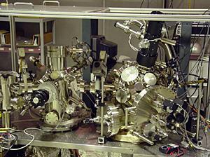
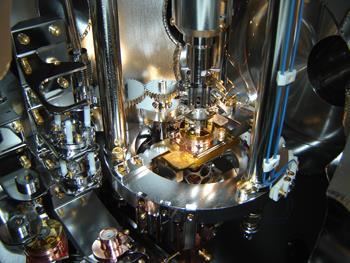
10 STM

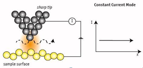
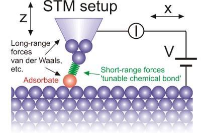
11 The principle of STM Probe Sample

12 The structure of STM I t ~ e -2kd
13 The manipulation of STM
 with")
14 Constant current image (topography) of an antiferromagnetic atomic layer iron on W(001) with defects and atoms.
15

")
16 1. Atomic imaging The Application of STM Nickel (110) Platinum (111)
 7nm x 7nm")
 surface 9nm x")
17 High performance STM image showing atomic resolution on Si(111) 7nm x 7nm cobalt sulfide "nanoflower" structure synthesized on a Au(111) surface 9nm x 9nm

18 2. Manipulation of single atoms and single molecules
19

20 Lateral manipulation: Transfer of atoms/molecules along surface using attractive/ repulsive forces between tip and atom/molecule. Vertical manipulation: Transfer of atoms/molecules between surface and STM tip using electronic/ vibration excitation by tunneling. Desorption: Similar to vertical manipulation, but desorption of atom/molecule into surrounding gas phase.


21 positioning 48 iron atoms into a ring in order to "corral" surface state electrons and force them into "quantum" state.

22 3. Single-molecular chemical reactions Dissociation: Selective bond breaking within a molecule by tunneling processes. Synthesis: Selective bond formation between two molecular units using lateral manipulation followed by electronic/vibration excitation.
.")
23 Schematic of bond formation in Au-PTCDA switch: In non-bonded state, atom and molecule are both negatively charged and stabilized by repulsive interaction (a). By tunneling out of molecular resonance, PTCDA is neutralized, and electrostatic repulsion is weakened (b). This makes Au atom moving towards molecule and form the bond.
 to form a single-molecule magnet.")
24 4. Construct molecular-level electronic device Terbium atom (red) is sandwiched between two organic molecules (grey and blue) to form a single-molecule magnet.
25 The advantages and disadvantages of STM Advantages: a 3D profile of a surface, allows to detect many features, including roughness, defects, and to determine size and conformation of molecules. Other advantages: obtain much more details than other microscopes, for a better understanding of research topics at molecular level. STM is versatile, it can be used in ultra-high vacuum, air, water and other liquids, and gas. can be operated in temperatures from zero Kelvin up to a few hundred degrees (Celsius).
26 Disadvantages: It is difficult to use STM effectively. It is a very specific technique that requires a lot of skill and precision. STM requires very stable and clean surfaces, excellent vibration control and sharp tips. STM only can be used to scan conducting samples which are not easily oxidized. STM uses highly specialized equipment that is expensive.

27 Atomic Force Microscope (AFM) Binnig, Quate and Gerber invented the first atomic force microscope


28 The structure of AFM Position Sensing Part Position Sensing photodetector Force Sensing Part Feedback circuit
29 The principle of AFM When a tip is close to sample, typically two forces operate: Coulombic and van der Waals interactions. The combination of these interactions results in a force-distance curve Coulombic Interaction: strong, short range repulsive force between tip and sample. This repulsion increases as the distance decreases. Van der Waals interactions: long range attractive force, which become obvious at distance of down to 10 nm.

30 As tip is brought towards the sample, van der Waals forces cause attraction. As tip gets closer to the sample this attraction increases. However at very small separations the repulsive coulombic force becomes dominant. The repulsive force causes the cantilever to bend when the tip is getting closer to the surface.
: Constant-height scan Constant-force")
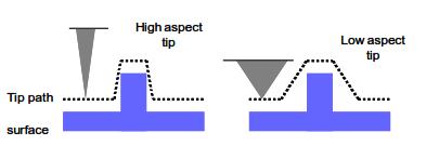
31 The manipulation of AFM Two scanning processes (contact mode): Constant-height scan Constant-force scan
32 Three AFM imaging modes: 1. Contact AFM < 0.5 nm probe-surface separation 2. Tapping mode AFM nm probe-surface separation 3. Non-contact AFM nm probe-surface separation
33 1. Contact AFM tip contacts the sample surface. The photo detector monitors the changing of cantilever deflection and the force is calculated using Hooke s law: F = k x (F = force, k = spring constant, x = cantilever deflection) The feedback circuit adjusts the probe height to maintain a constant force and deflection on the cantilever, i.e. deflection setpoint. Constant-force scan
34 2. Tapping mode AFM (Intermittent contact ) cantilever oscillates at (or slightly below) its resonant frequency. Oscillation amplitude ranges in nm. Tip lightly touch ( taps ) on sample surface during scanning. Resonant frequency of cantilever dependent on tip/surface separation. Oscillation decreases when tip is closer to surface. Hence changes of oscillation amplitude are used for measuring tip/surface separation. Feedback circuit adjusts probe height to maintain a constant amplitude of oscillation. i.e. the amplitude setpoint. Constant-height scan
35 Tapping mode in air: A small piezoelectric crystal on AFM tip holder makes the cantilever oscillate up and down. Tapping mode in liquids: Tapping mode operation in liquids is a very useful tool for biologists.

36 3. Non-contact AFM cantilever oscillate near sample surface, but does not contact it. Oscillation is at slightly above resonant frequency. Van der Waals force decrease resonant frequency. This decrease of resonant frequency causes oscillation amplitude to decrease. Normally adsorbed fluidic layer is much thicker than the dominant region of van der Waals force - probe is either out of range of van der Waals force, or becomes trapped in fluidic layer. Therefore noncontact mode AFM works best under ultra-high vacuum conditions.
37 The Properties of the different operation modes in AFM.
. - Lower forces, less damage to soft samples in air. - Almost no lateral forces.")
38 Advantages and Disadvantages of AFM Modes Contact Mode Tapping Mode Noncontact Mode Advantage - High scan speeds - Atomic resolution possible - Easier scanning of rough samples with large changes in vertical topography. - High lateral resolution (1 to 5 nm). - Lower forces, less damage to soft samples in air. - Almost no lateral forces. - Both normal and lateral forces are minimised, good for measuring very soft samples - Can get atomic resolution in UHV environment Disadvantage Lateral forces distort image Combination of forces reduces spatial resolution and cause damage to soft samples. Slower scan speed than contact mode Slower scan speed than tapping and contact modes Lower lateral resolution, limited by tip-sample separation. Usually only applicable in extremely hydrophobic samples with a minimium fluidic layer.


39 1. Imaging The application of AFM AFM 3D image of a detail of the free surface of an artificial pattern The figure illustrates 800 nm wide and 10 nm high Pd/Fe/Pd thin film dots fabricated using electron lithography.

 surface, 4.")

40 PMMA spheres scanning range 45x45 μm NCAFM image of the Ge/Si(105) surface, 4.2 nm x 4.2 nm AFM image of human plasma sample (fibrinogen)
 http://www.youtube.com/watch?")
41 2. Measuring forces (and mechanical properties) at nanoscale Illustration of an AFM tip measuring the force to move a cobalt atom on a crystalline surface. (Credit: Image courtesy of IBM)

42 Single-molecule force microscope uses a target molecule at AFM tip end to probe surface molecules with a strong attractive force. Force measurements are mapped as an image.
, at nano-scale grab and")

43 3. As a nanoscale tool bending, cutting and extracting soft materials (Polymers, DNA, nanotubes), at nano-scale grab and hold a nanoparticle in a position Manipulating nanotube on Si substrate. AFM tip creates Greek letter "theta" from a 2.5 μm long nanotube
, finally stretched across an tungsten oxide barrier")
44 A single nanotube (red) on an insulating substrate (SiO2, green) is manipulated in a few steps onto a W film thin wire (blue), finally stretched across an tungsten oxide barrier (yellow).
45 The advantage and disadvantage of AFM Advantages : 1) high-resolution 3-D surface images 2) not require special sample treatments (no sample's destruction) 3) Usually not require vacuum (operate both in air and liquid); 4) could be used for organic materials Disadvantages: 1) image size is much smaller than that of electron microscopes; 2) slow scanning rate, unlike an electron microscope which does it in almost real-time. 3) tip convolution -- not true sample topography 4) expensive tips
")
 appear narrower than")
46 Tip convolution----tip Related Artifacts protrusions (dots) appear wider, depressions (pores) appear narrower than the reality.

47

48 AFM Section Analysis of the nano-discs, the average height and size of the nano-discs are approximately 1.5 and 80 nm, respectively.

49 AFM Section Analysis of the nano-hemisphere. To accurately reflect the shape of the nanoparticles, we used the same dimension scale for the horizontal and vertical coordinates. The average height and base diameter of the nanohemispheres are approximately and 75 nm, respectively.

50 AFM Section Analysis of the nano-hemiellipsoids. To accurately reflect the shape of the nanoparticles, we used the same dimension scale for the horizontal and vertical coordinates. The average height and base diameter of the nanohemiellipsoids are approximately and 65 nm, respectively.

51 AFM Section Analysis of the nano-conics. To accurately reflect the shape of the nanoparticles, we used the same dimension scale for the horizontal and vertical coordinates. The average height and base diameter of the nano-conics are approximately and 60 nm, respectively.
52 Thank you and have a nice day!
Techniken der Oberflächenphysik (Techniques of Surface Physics)
") Techniken der Oberflächenphysik (Techniques of Surface Physics) Prof. Yong Lei Dr. Ynag Xu and Mr. Grote Fabian Fachgebiet 3D-Nanostrukturierung, Institut für Physik Contact: yong.lei@tu-ilmenau.de; yang.xu@tu-ilmenau.de
Techniken der Oberflächenphysik (Techniques of Surface Physics) Prof. Yong Lei Dr. Ynag Xu and Mr. Grote Fabian Fachgebiet 3D-Nanostrukturierung, Institut für Physik Contact: yong.lei@tu-ilmenau.de; yang.xu@tu-ilmenau.de
Techniken der Oberflächenphysik (Technique of Surface Physics)
") Techniken der Oberflächenphysik (Technique of Surface Physics) Yong Lei & Fabian Grote Fachgebiet 3D-Nanostrukturierung, Institut für Physik Contact: yong.lei@tu-ilmenau.de; fabian.grote@tu-ilmenau.de
Techniken der Oberflächenphysik (Technique of Surface Physics) Yong Lei & Fabian Grote Fachgebiet 3D-Nanostrukturierung, Institut für Physik Contact: yong.lei@tu-ilmenau.de; fabian.grote@tu-ilmenau.de
Contents. What is AFM? History Basic principles and devices Operating modes Application areas Advantages and disadvantages
 Contents What is AFM? History Basic principles and devices Operating modes Application areas Advantages and disadvantages Figure1: 2004 Seth Copen Goldstein What is AFM? A type of Scanning Probe Microscopy
Techniken der Oberflächenphysik (Techniques of Surface Physics)
") Techniken der Oberflächenphysik (Techniques of Surface Physics) Prof. Yong Lei & Dr. Yang Xu, Dr. Huaping Zhao Fachgebiet Angewante Nanophysik, Institut für Physik Contact: yong.lei@tu-ilmenau.de yang.xu@tu-ilmenau.de
Techniken der Oberflächenphysik (Techniques of Surface Physics) Prof. Yong Lei & Dr. Yang Xu, Dr. Huaping Zhao Fachgebiet Angewante Nanophysik, Institut für Physik Contact: yong.lei@tu-ilmenau.de yang.xu@tu-ilmenau.de
General concept and defining characteristics of AFM. Dina Kudasheva Advisor: Prof. Mary K. Cowman
 General concept and defining characteristics of AFM Dina Kudasheva Advisor: Prof. Mary K. Cowman Overview Introduction History of the SPM invention Technical Capabilities Principles of operation Examples
Scanning Probe Microscopy. EMSE-515 F. Ernst
 Scanning Probe Microscopy EMSE-515 F. Ernst 1 Literature 2 3 Scanning Probe Microscopy: The Lab on a Tip by Ernst Meyer,Ans Josef Hug,Roland Bennewitz 4 Scanning Probe Microscopy and Spectroscopy : Theory,
Basic Laboratory. Materials Science and Engineering. Atomic Force Microscopy (AFM)
") Basic Laboratory Materials Science and Engineering Atomic Force Microscopy (AFM) M108 Stand: 20.10.2015 Aim: Presentation of an application of the AFM for studying surface morphology. Inhalt 1.Introduction...
Basic Laboratory Materials Science and Engineering Atomic Force Microscopy (AFM) M108 Stand: 20.10.2015 Aim: Presentation of an application of the AFM for studying surface morphology. Inhalt 1.Introduction...
Lecture 4 Scanning Probe Microscopy (SPM)
") Lecture 4 Scanning Probe Microscopy (SPM) General components of SPM; Tip --- the probe; Cantilever --- the indicator of the tip; Tip-sample interaction --- the feedback system; Scanner --- piezoelectric
Lecture 4 Scanning Probe Microscopy (SPM) General components of SPM; Tip --- the probe; Cantilever --- the indicator of the tip; Tip-sample interaction --- the feedback system; Scanner --- piezoelectric
Imaging Methods: Scanning Force Microscopy (SFM / AFM)
") Imaging Methods: Scanning Force Microscopy (SFM / AFM) The atomic force microscope (AFM) probes the surface of a sample with a sharp tip, a couple of microns long and often less than 100 Å in diameter.
Imaging Methods: Scanning Force Microscopy (SFM / AFM) The atomic force microscope (AFM) probes the surface of a sample with a sharp tip, a couple of microns long and often less than 100 Å in diameter.
Program Operacyjny Kapitał Ludzki SCANNING PROBE TECHNIQUES - INTRODUCTION
 Program Operacyjny Kapitał Ludzki SCANNING PROBE TECHNIQUES - INTRODUCTION Peter Liljeroth Department of Applied Physics, Aalto University School of Science peter.liljeroth@aalto.fi Projekt współfinansowany
Chapter 10. Nanometrology. Oxford University Press All rights reserved.
 Chapter 10 Nanometrology Oxford University Press 2013. All rights reserved. 1 Introduction Nanometrology is the science of measurement at the nanoscale level. Figure illustrates where nanoscale stands
Techniken der Oberflächenphysik (Techniques of Surface Physics)
") Techniken der Oberflächenphysik (Techniques of Surface Physics) Prof. Yong Lei & Dr. Yang Xu (& Liying Liang) Fachgebiet 3D-Nanostrukturierung, Institut für Physik Contact: yong.lei@tu-ilmenau.de; yang.xu@tu-ilmenau.de;
Techniken der Oberflächenphysik (Techniques of Surface Physics) Prof. Yong Lei & Dr. Yang Xu (& Liying Liang) Fachgebiet 3D-Nanostrukturierung, Institut für Physik Contact: yong.lei@tu-ilmenau.de; yang.xu@tu-ilmenau.de;
Scanning Probe Microscopy. Amanda MacMillan, Emmy Gebremichael, & John Shamblin Chem 243: Instrumental Analysis Dr. Robert Corn March 10, 2010
 Scanning Probe Microscopy Amanda MacMillan, Emmy Gebremichael, & John Shamblin Chem 243: Instrumental Analysis Dr. Robert Corn March 10, 2010 Scanning Probe Microscopy High-Resolution Surface Analysis
From nanophysics research labs to cell phones. Dr. András Halbritter Department of Physics associate professor
 From nanophysics research labs to cell phones Dr. András Halbritter Department of Physics associate professor Curriculum Vitae Birth: 1976. High-school graduation: 1994. Master degree: 1999. PhD: 2003.
Characterization Tools
 Lectures in Nanoscience & Technology Characterization Tools K. Sakkaravarthi Department of Physics National Institute of Technology Tiruchirappalli 620 015 Tamil Nadu India sakkaravarthi@nitt.edu ksakkaravarthi.weebly.com
Outline Scanning Probe Microscope (SPM)
") AFM Outline Scanning Probe Microscope (SPM) A family of microscopy forms where a sharp probe is scanned across a surface and some tip/sample interactions are monitored Scanning Tunneling Microscopy (STM)
AFM Outline Scanning Probe Microscope (SPM) A family of microscopy forms where a sharp probe is scanned across a surface and some tip/sample interactions are monitored Scanning Tunneling Microscopy (STM)
Module 26: Atomic Force Microscopy. Lecture 40: Atomic Force Microscopy 3: Additional Modes of AFM
 Module 26: Atomic Force Microscopy Lecture 40: Atomic Force Microscopy 3: Additional Modes of AFM 1 The AFM apart from generating the information about the topography of the sample features can be used
Atomic Force Microscopy imaging and beyond
 Atomic Force Microscopy imaging and beyond Arif Mumtaz Magnetism and Magnetic Materials Group Department of Physics, QAU Coworkers: Prof. Dr. S.K.Hasanain M. Tariq Khan Alam Imaging and beyond Scanning
Introduction to Scanning Probe Microscopy Zhe Fei
 Introduction to Scanning Probe Microscopy Zhe Fei Phys 590B, Apr. 2019 1 Outline Part 1 SPM Overview Part 2 Scanning tunneling microscopy Part 3 Atomic force microscopy Part 4 Electric & Magnetic force
STM: Scanning Tunneling Microscope
 STM: Scanning Tunneling Microscope Basic idea STM working principle Schematic representation of the sample-tip tunnel barrier Assume tip and sample described by two infinite plate electrodes Φ t +Φ s =
Ecole Franco-Roumaine : Magnétisme des systèmes nanoscopiques et structures hybrides - Brasov, Modern Analytical Microscopic Tools
 1. Introduction Solid Surfaces Analysis Group, Institute of Physics, Chemnitz University of Technology, Germany 2. Limitations of Conventional Optical Microscopy 3. Electron Microscopies Transmission Electron
Scanning Tunneling Microscopy
 Scanning Tunneling Microscopy References: 1. G. Binnig, H. Rohrer, C. Gerber, and Weibel, Phys. Rev. Lett. 49, 57 (1982); and ibid 50, 120 (1983). 2. J. Chen, Introduction to Scanning Tunneling Microscopy,
SOLID STATE PHYSICS PHY F341. Dr. Manjuladevi.V Associate Professor Department of Physics BITS Pilani
 SOLID STATE PHYSICS PHY F341 Dr. Manjuladevi.V Associate Professor Department of Physics BITS Pilani 333031 manjula@bits-pilani.ac.in Characterization techniques SEM AFM STM BAM Outline What can we use
MS482 Materials Characterization ( 재료분석 ) Lecture Note 11: Scanning Probe Microscopy. Byungha Shin Dept. of MSE, KAIST
 Lecture Note 11: Scanning Probe Microscopy. Byungha Shin Dept. of MSE, KAIST") 2015 Fall Semester MS482 Materials Characterization ( 재료분석 ) Lecture Note 11: Scanning Probe Microscopy Byungha Shin Dept. of MSE, KAIST 1 Course Information Syllabus 1. Overview of various characterization
2015 Fall Semester MS482 Materials Characterization ( 재료분석 ) Lecture Note 11: Scanning Probe Microscopy Byungha Shin Dept. of MSE, KAIST 1 Course Information Syllabus 1. Overview of various characterization
Atomic Force Microscopy (AFM) Part I
 Part I") Atomic Force Microscopy (AFM) Part I CHEM-L2000 Eero Kontturi 6 th March 2018 Lectures on AFM Part I Principles and practice Imaging of native materials, including nanocellulose Part II Surface force measurements
Atomic Force Microscopy (AFM) Part I CHEM-L2000 Eero Kontturi 6 th March 2018 Lectures on AFM Part I Principles and practice Imaging of native materials, including nanocellulose Part II Surface force measurements
Introduction to Scanning Probe Microscopy
 WORKSHOP Nanoscience on the Tip Introduction to Scanning Probe Microscopy Table of Contents: 1 Historic Perspectives... 1 2 Scanning Force Microscopy (SFM)... 2 2.1. Contact Mode... 2 2.2. AC Mode Imaging...
Scanning Force Microscopy
 Scanning Force Microscopy Roland Bennewitz Rutherford Physics Building 405 Phone 398-3058 roland.bennewitz@mcgill.ca Scanning Probe is moved along scan lines over a sample surface 1 Force Microscopy Data
Scanning Probe Microscopy (SPM)
") CHEM53200: Lecture 9 Scanning Probe Microscopy (SPM) Major reference: 1. Scanning Probe Microscopy and Spectroscopy Edited by D. Bonnell (2001). 2. A practical guide to scanning probe microscopy by Park
CHEM53200: Lecture 9 Scanning Probe Microscopy (SPM) Major reference: 1. Scanning Probe Microscopy and Spectroscopy Edited by D. Bonnell (2001). 2. A practical guide to scanning probe microscopy by Park
Nanostrukturphysik (Nanostructure Physics)
") Nanostrukturphysik (Nanostructure Physics) Prof. Yong Lei & Dr. Yang Xu Fachgebiet 3D-Nanostrukturierung, Institut für Physik Contact: yong.lei@tu-ilmenau.de; yang.xu@tu-ilmenau.de Office: Unterpoerlitzer
Nanostrukturphysik (Nanostructure Physics) Prof. Yong Lei & Dr. Yang Xu Fachgebiet 3D-Nanostrukturierung, Institut für Physik Contact: yong.lei@tu-ilmenau.de; yang.xu@tu-ilmenau.de Office: Unterpoerlitzer
Atomic and molecular interactions. Scanning probe microscopy.
 Atomic and molecular interactions. Scanning probe microscopy. Balázs Kiss Nanobiotechnology and Single Molecule Research Group, Department of Biophysics and Radiation Biology 27. November 2013. 2 Atomic
Characterization of MEMS Devices
 MEMS: Characterization Characterization of MEMS Devices Prasanna S. Gandhi Assistant Professor, Department of Mechanical Engineering, Indian Institute of Technology, Bombay, Recap Characterization of MEMS
Scanning Probe Microscopy (SPM)
") http://ww2.sljus.lu.se/staff/rainer/spm.htm Scanning Probe Microscopy (FYST42 / FAFN30) Scanning Probe Microscopy (SPM) overview & general principles March 23 th, 2018 Jan Knudsen, room K522, jan.knudsen@sljus.lu.se
http://ww2.sljus.lu.se/staff/rainer/spm.htm Scanning Probe Microscopy (FYST42 / FAFN30) Scanning Probe Microscopy (SPM) overview & general principles March 23 th, 2018 Jan Knudsen, room K522, jan.knudsen@sljus.lu.se
Chapter 12. Nanometrology. Oxford University Press All rights reserved.
 Chapter 12 Nanometrology Introduction Nanometrology is the science of measurement at the nanoscale level. Figure illustrates where nanoscale stands in relation to a meter and sub divisions of meter. Nanometrology
CHARACTERIZATION of NANOMATERIALS KHP
 CHARACTERIZATION of NANOMATERIALS Overview of the most common nanocharacterization techniques MAIN CHARACTERIZATION TECHNIQUES: 1.Transmission Electron Microscope (TEM) 2. Scanning Electron Microscope
MSE 321 Structural Characterization
 Auger Spectroscopy Auger Electron Spectroscopy (AES) Scanning Auger Microscopy (SAM) Incident Electron Ejected Electron Auger Electron Initial State Intermediate State Final State Physical Electronics
AFM for Measuring Surface Topography and Forces
 ENB 2007 07.03.2007 AFM for Measuring Surface Topography and Forces Andreas Fery Scanning Probe : What is it and why do we need it? AFM as a versatile tool for local analysis and manipulation Dates Course
672 Advanced Solid State Physics. Scanning Tunneling Microscopy
 672 Advanced Solid State Physics Scanning Tunneling Microscopy Biao Hu Outline: 1. Introduction to STM 2. STM principle & working modes 3. STM application & extension 4. STM in our group 1. Introduction
MSE 321 Structural Characterization
 Auger Spectroscopy Auger Electron Spectroscopy (AES) Scanning Auger Microscopy (SAM) Incident Electron Ejected Electron Auger Electron Initial State Intermediate State Final State Physical Electronics
Instrumentation and Operation
 Instrumentation and Operation 1 STM Instrumentation COMPONENTS sharp metal tip scanning system and control electronics feedback electronics (keeps tunneling current constant) image processing system data
NIS: what can it be used for?
 AFM @ NIS: what can it be used for? Chiara Manfredotti 011 670 8382/8388/7879 chiara.manfredotti@to.infn.it Skype: khiaram 1 AFM: block scheme In an Atomic Force Microscope (AFM) a micrometric tip attached
Scanning Tunneling Microscopy
 Scanning Tunneling Microscopy Scanning Direction References: Classical Tunneling Quantum Mechanics Tunneling current Tunneling current I t I t (V/d)exp(-Aφ 1/2 d) A = 1.025 (ev) -1/2 Å -1 I t = 10 pa~10na
Nanostructure. Materials Growth Characterization Fabrication. More see Waser, chapter 2
 Nanostructure Materials Growth Characterization Fabrication More see Waser, chapter 2 Materials growth - deposition deposition gas solid Physical Vapor Deposition Chemical Vapor Deposition Physical Vapor
Final Reading Assignment: Travels to the Nanoworld: pages pages pages
 Final Reading Assignment: Travels to the Nanoworld: pages 152-164 pages 201-214 pages 219-227 Bottom-up nanofabrication Can we assemble nanomachines manually? What are the components (parts)? nanoparticles
Lecture 26 MNS 102: Techniques for Materials and Nano Sciences
 Lecture 26 MNS 102: Techniques for Materials and Nano Sciences Reference: #1 C. R. Brundle, C. A. Evans, S. Wilson, "Encyclopedia of Materials Characterization", Butterworth-Heinemann, Toronto (1992),
CH676 Physical Chemistry: Principles and Applications. CH676 Physical Chemistry: Principles and Applications
 CH676 Physical Chemistry: Principles and Applications History of Nanotechnology: Time Line Democritus in ancient Greece: concept of atom 1900 : Rutherford : discovery of atomic nucleus The first TEM was
tip of a current tip and the sample. Components: 3. Coarse sample-to-tip isolation system, and
 SCANNING TUNNELING MICROSCOPE Brief history: Heinrich Rohrer and Gerd K. Binnig, scientists at IBM's Zurich Research Laboratory in Switzerland, are awarded the 1986 Nobel Prize in physicss for their work
Techniken der Oberflächenphysik
 Techniken der Oberflächenphysik Prof. Yong Lei & Dr. Yang Xu Fachgebiet 3D-Nanostrukturierung, Institut für Physik 18.01.2018 Contact: yong.lei@tu-ilmenau.de; yang.xu@tu-ilmenau.de Office: Heisenbergbau
Nanotechnology Fabrication Methods.
 Nanotechnology Fabrication Methods. 10 / 05 / 2016 1 Summary: 1.Introduction to Nanotechnology:...3 2.Nanotechnology Fabrication Methods:...5 2.1.Top-down Methods:...7 2.2.Bottom-up Methods:...16 3.Conclusions:...19
= 6 (1/ nm) So what is probability of finding electron tunneled into a barrier 3 ev high?
 So what is probability of finding electron tunneled into a barrier 3 ev high?") STM STM With a scanning tunneling microscope, images of surfaces with atomic resolution can be readily obtained. An STM uses quantum tunneling of electrons to map the density of electrons on the surface
STM STM With a scanning tunneling microscope, images of surfaces with atomic resolution can be readily obtained. An STM uses quantum tunneling of electrons to map the density of electrons on the surface
Understanding the properties and behavior of groups of interacting atoms more than simple molecules
 Condensed Matter Physics Scratching the Surface Understanding the properties and behavior of groups of interacting atoms more than simple molecules Solids and fluids in ordinary and exotic states low energy
REPORT ON SCANNING TUNNELING MICROSCOPE. Course ME-228 Materials and Structural Property Correlations Course Instructor Prof. M. S.
 REPORT ON SCANNING TUNNELING MICROSCOPE Course ME-228 Materials and Structural Property Correlations Course Instructor Prof. M. S. Bobji Submitted by Ankush Kumar Jaiswal (09371) Abhay Nandan (09301) Sunil
AFM Imaging In Liquids. W. Travis Johnson PhD Agilent Technologies Nanomeasurements Division
 AFM Imaging In Liquids W. Travis Johnson PhD Agilent Technologies Nanomeasurements Division Imaging Techniques: Scales Proteins 10 nm Bacteria 1μm Red Blood Cell 5μm Human Hair 75μm Si Atom Spacing 0.4nm
Lecture 12: Biomaterials Characterization in Aqueous Environments
 3.051J/20.340J 1 Lecture 12: Biomaterials Characterization in Aqueous Environments High vacuum techniques are important tools for characterizing surface composition, but do not yield information on surface
Scanning Probe Microscopy
 1 Scanning Probe Microscopy Dr. Benjamin Dwir Laboratory of Physics of Nanostructures (LPN) Benjamin.dwir@epfl.ch PH.D3.344 Outline: Introduction: What is SPM, history STM AFM Image treatment Advanced
INDIAN INSTITUTE OF TECHNOLOGY ROORKEE NPTEL NPTEL ONLINE CERTIFICATION COURSE. Biomedical Nanotechnology. Lec-05 Characterisation of Nanoparticles
 INDIAN INSTITUTE OF TECHNOLOGY ROORKEE NPTEL NPTEL ONLINE CERTIFICATION COURSE Biomedical Nanotechnology Lec-05 Characterisation of Nanoparticles Dr. P. Gopinath Department of Biotechnology Indian Institute
And Manipulation by Scanning Probe Microscope
 Basic 15 Nanometer Scale Measurement And Manipulation by Scanning Probe Microscope Prof. K. Fukuzawa Dept. of Micro/Nano Systems Engineering Nagoya University I. Basics of scanning probe microscope Basic
Scanning Tunneling Microscopy Transmission Electron Microscopy
 Scanning Tunneling Microscopy Transmission Electron Microscopy Speakers Burcu Başar Semih Gezgin Yavuz Selim Telis Place Hacettepe University Department of Chemical Engineering It s a small world after
Scanning Probe Microscopies (SPM)
") Scanning Probe Microscopies (SPM) Nanoscale resolution af objects at solid surfaces can be reached with scanning probe microscopes. They allow to record an image of the surface atomic arrangement in direct
Scanning Probe Microscopies (SPM) Nanoscale resolution af objects at solid surfaces can be reached with scanning probe microscopes. They allow to record an image of the surface atomic arrangement in direct
Nanostrukturphysik (Nanostructure Physics)
") Nanostrukturphysik (Nanostructure Physics) Prof. Yong Lei & Dr. Yang Xu Fachgebiet 3D-Nanostrukturierung, Institut für Physik Contact: yong.lei@tu-ilmenau.de; yang.xu@tu-ilmenau.de Office: Unterpoerlitzer
Nanostrukturphysik (Nanostructure Physics) Prof. Yong Lei & Dr. Yang Xu Fachgebiet 3D-Nanostrukturierung, Institut für Physik Contact: yong.lei@tu-ilmenau.de; yang.xu@tu-ilmenau.de Office: Unterpoerlitzer
INTRODUCTION TO SCA\ \I\G TUNNELING MICROSCOPY
 INTRODUCTION TO SCA\ \I\G TUNNELING MICROSCOPY SECOND EDITION C. JULIAN CHEN Department of Applied Physics and Applied Mathematics, Columbia University, New York OXFORD UNIVERSITY PRESS Contents Preface
Intermittent-Contact Mode Force Microscopy & Electrostatic Force Microscopy (EFM)
") WORKSHOP Nanoscience on the Tip Intermittent-Contact Mode Force Microscopy & Electrostatic Force Microscopy (EFM) Table of Contents: 1. Motivation... 1. Simple Harmonic Motion... 1 3. AC-Mode Imaging...
WORKSHOP Nanoscience on the Tip Intermittent-Contact Mode Force Microscopy & Electrostatic Force Microscopy (EFM) Table of Contents: 1. Motivation... 1. Simple Harmonic Motion... 1 3. AC-Mode Imaging...
CNPEM Laboratório de Ciência de Superfícies
 Investigating electrical charged samples by scanning probe microscopy: the influence to magnetic force microscopy and atomic force microscopy phase images. Carlos A. R. Costa, 1 Evandro M. Lanzoni, 1 Maria
Scanning Probe Microscopy (SPM)
") Scanning Probe Microscopy (SPM) Scanning Tunneling Microscopy (STM) --- G. Binnig, H. Rohrer et al, (1982) Near-Field Scanning Optical Microscopy (NSOM) --- D. W. Pohl (1982) Atomic Force Microscopy (AFM)
Scanning Probe Microscopy (SPM) Scanning Tunneling Microscopy (STM) --- G. Binnig, H. Rohrer et al, (1982) Near-Field Scanning Optical Microscopy (NSOM) --- D. W. Pohl (1982) Atomic Force Microscopy (AFM)
Università degli Studi di Bari "Aldo Moro"
 Università degli Studi di Bari "Aldo Moro" Table of contents 1. Introduction to Atomic Force Microscopy; 2. Introduction to Raman Spectroscopy; 3. The need for a hybrid technique Raman AFM microscopy;
Citation for published version (APA): Mendoza, S. M. (2007). Exploiting molecular machines on surfaces s.n.
: Mendoza, S. M. (2007). Exploiting molecular machines on surfaces s.n.") University of Groningen Exploiting molecular machines on surfaces Mendoza, Sandra M IMPORTANT NOTE: You are advised to consult the publisher's version (publisher's PDF) if you wish to cite from it. Please
University of Groningen Exploiting molecular machines on surfaces Mendoza, Sandra M IMPORTANT NOTE: You are advised to consult the publisher's version (publisher's PDF) if you wish to cite from it. Please
Quantum Condensed Matter Physics Lecture 12
 Quantum Condensed Matter Physics Lecture 12 David Ritchie QCMP Lent/Easter 2016 http://www.sp.phy.cam.ac.uk/drp2/home 12.1 QCMP Course Contents 1. Classical models for electrons in solids 2. Sommerfeld
Lesson 4: Tools of the Nanosciences. Student Materials
 Lesson 4: Tools of the Nanosciences Student Materials Contents Black Box Lab Activity: Student Instructions and Worksheet Seeing and Building Small Things: Student Reading Seeing and Building Small Things:
Seminars in Nanosystems - I
 Seminars in Nanosystems - I Winter Semester 2011/2012 Dr. Emanuela Margapoti Emanuela.Margapoti@wsi.tum.de Dr. Gregor Koblmüller Gregor.Koblmueller@wsi.tum.de Seminar Room at ZNN 1 floor Topics of the
Scanning Force Microscopy II
 Scanning Force Microscopy II Measurement modes Magnetic force microscopy Artifacts Lars Johansson 1 SFM - Forces Chemical forces (short range) Van der Waals forces Electrostatic forces (long range) Capillary
Integrating MEMS Electro-Static Driven Micro-Probe and Laser Doppler Vibrometer for Non-Contact Vibration Mode SPM System Design
 Tamkang Journal of Science and Engineering, Vol. 12, No. 4, pp. 399 407 (2009) 399 Integrating MEMS Electro-Static Driven Micro-Probe and Laser Doppler Vibrometer for Non-Contact Vibration Mode SPM System
MRSEC. Refrigerator Magnet Activity Guide. Quick Reference Activity Guide. a) b) c) = north = south. Activity Materials
 b) c) = north = south. Activity Materials") MRSEC Refrigerator Magnet Activity Guide Quick Reference Activity Guide Activity Materials Refrigerator magnet with removable probe strip Magnetic field diagrams Starting Points One of the great breakthroughs
MRSEC Refrigerator Magnet Activity Guide Quick Reference Activity Guide Activity Materials Refrigerator magnet with removable probe strip Magnetic field diagrams Starting Points One of the great breakthroughs
MAGNETIC FORCE MICROSCOPY
 University of Ljubljana Faculty of Mathematics and Physics Department of Physics SEMINAR MAGNETIC FORCE MICROSCOPY Author: Blaž Zupančič Supervisor: dr. Igor Muševič February 2003 Contents 1 Abstract 3
bio-molecular studies Physical methods in Semmelweis University Osváth Szabolcs
 Physical methods in bio-molecular studies Osváth Szabolcs Semmelweis University szabolcs.osvath@eok.sote.hu Light emission and absorption spectra Stokes shift is the difference (in wavelength or frequency
Chapter 5 Nanomanipulation. Chapter 5 Nanomanipulation. 5.1: With a nanotube. Cutting a nanotube. Moving a nanotube
 Objective: learn about nano-manipulation techniques with a STM or an AFM. 5.1: With a nanotube Moving a nanotube Cutting a nanotube Images at large distance At small distance : push the NT Voltage pulse
Probing Molecular Electronics with Scanning Probe Microscopy
 Probing Molecular Electronics with Scanning Probe Microscopy Mark C. Hersam Assistant Professor Department of Materials Science and Engineering, Northwestern University, Evanston, IL 60208-3108 Ph: 847-491-2696,
Microscopie a stilo: principi ed esempi di applicazione
 Microscopie a stilo: principi ed esempi di applicazione Adele Sassella Dipartimento di Scienza dei Materiali Università degli Studi di Milano Bicocca adele.sassella@unimib.it Pavia, 22 aprile 2009 SCANNING
Laserphysik. Prof. Yong Lei & Dr. Yang Xu. Fachgebiet Angewandte Nanophysik, Institut für Physik
 Laserphysik Prof. Yong Lei & Dr. Yang Xu Fachgebiet Angewandte Nanophysik, Institut für Physik Contact: yong.lei@tu-ilmenau.de; yang.xu@tu-ilmenau.de Office: Heisenbergbau V 202, Unterpörlitzer Straße
MATERIAL SCIENCE AND TECHONOLOGY-1. Scanning Tunneling Microscope, STM Tunneling Electron Microscope, TEM HATİCE DOĞRUOĞLU
 MATERIAL SCIENCE AND TECHONOLOGY-1 Scanning Tunneling Microscope, STM Tunneling Electron Microscope, TEM HATİCE DOĞRUOĞLU Scanning Tunelling Microscope (STM) In 1981,Gerd Binnig and Heinrich Rohrer and
Atomic Force Microscopy
 Journal of the Advanced Undergraduate Physics Laboratory Investigation Volume 0 Issue 0 Premiere Issue Article 2 6-6-2012 Atomic Force Microscopy Tyler Lane Minnesota State University - Moorhead, lanety@mnstate.edu
Scanning Tunneling Microscopy
 Scanning Tunneling Microscopy A scanning tunneling microscope (STM) is an instrument for imaging surfaces at the atomic level. Its development in 1981 earned its inventors, Gerd Binnig and Heinrich Rohrer
Nanostrukturphysik (Nanostructure Physics)
") Nanostrukturphysik (Nanostructure Physics) Yong Lei & Fabian Grote Fachgebiet 3D-Nanostrukturierung, Institut für Physik Contact: yong.lei@tu-ilmenau.de; fabian.grote@tu-ilmenau.de Office: Heliosbau 1102,
Nanostrukturphysik (Nanostructure Physics) Yong Lei & Fabian Grote Fachgebiet 3D-Nanostrukturierung, Institut für Physik Contact: yong.lei@tu-ilmenau.de; fabian.grote@tu-ilmenau.de Office: Heliosbau 1102,
Nanostrukturphysik (Nanostructure Physics)
") Nanostrukturphysik (Nanostructure Physics) Prof. Yong Lei & Dr. Huaping Zhao Fachgebiet Angewandte Nanophysik, Institut für Physik Contact: yong.lei@tu-ilmenau.de; huaping.zhao@tu-ilmenau.de Office: Unterpoerlitzer
Nanostrukturphysik (Nanostructure Physics) Prof. Yong Lei & Dr. Huaping Zhao Fachgebiet Angewandte Nanophysik, Institut für Physik Contact: yong.lei@tu-ilmenau.de; huaping.zhao@tu-ilmenau.de Office: Unterpoerlitzer
Sensors of Structure. debroglie. Wave-Particle duality. Bragg reflection. Electron Diffraction. Heisenberg Uncertantity Principle
 Sensors of Structure Matter Waves and the debroglie wavelength Heisenberg uncertainty principle Electron diffraction Transmission electron microscopy Atomic-resolution sensors debroglie Postulated that
Scanning Tunneling Microscopy and its Application
 Chunli Bai Scanning Tunneling Microscopy and its Application With 181 Figures SHANGHAI SCIENTIFIC & TECHNICAL PUBLISHERS Jpl Springer Contents 1. Introduction 1 1.1 Advantages of STM Compared with Other
SCANNING-PROBE TECHNIQUES OR APPARATUS; APPLICATIONS OF SCANNING-PROBE TECHNIQUES, e.g. SCANNING PROBE MICROSCOPY [SPM]
![SCANNING-PROBE TECHNIQUES OR APPARATUS; APPLICATIONS OF SCANNING-PROBE TECHNIQUES, e.g. SCANNING PROBE MICROSCOPY [SPM]](/thumbs/81/83165631.jpg "SCANNING-PROBE TECHNIQUES OR APPARATUS; APPLICATIONS OF SCANNING-PROBE TECHNIQUES, e.g. SCANNING PROBE MICROSCOPY [SPM]") G01Q SCANNING-PROBE TECHNIQUES OR APPARATUS; APPLICATIONS OF SCANNING-PROBE TECHNIQUES, e.g. SCANNING PROBE MICROSCOPY [SPM] Scanning probes, i.e. devices having at least a tip of nanometre sized dimensions
G01Q SCANNING-PROBE TECHNIQUES OR APPARATUS; APPLICATIONS OF SCANNING-PROBE TECHNIQUES, e.g. SCANNING PROBE MICROSCOPY [SPM] Scanning probes, i.e. devices having at least a tip of nanometre sized dimensions
Nitride HFETs applications: Conductance DLTS
 Nitride HFETs applications: Conductance DLTS The capacitance DLTS cannot be used for device trap profiling as the capacitance for the gate will be very small Conductance DLTS is similar to capacitance
Kavli Workshop for Journalists. June 13th, CNF Cleanroom Activities
 Kavli Workshop for Journalists June 13th, 2007 CNF Cleanroom Activities Seeing nm-sized Objects with an SEM Lab experience: Scanning Electron Microscopy Equipment: Zeiss Supra 55VP Scanning electron microscopes
Initial Stages of Growth of Organic Semiconductors on Graphene
 Initial Stages of Growth of Organic Semiconductors on Graphene Presented by: Manisha Chhikara Supervisor: Prof. Dr. Gvido Bratina University of Nova Gorica Outline Introduction to Graphene Fabrication
Nanotechnology Nanofabrication of Functional Materials. Marin Alexe Max Planck Institute of Microstructure Physics, Halle - Germany
 Nanotechnology Nanofabrication of Functional Materials Marin Alexe Max Planck Institute of Microstructure Physics, Halle - Germany Contents Part I History and background to nanotechnology Nanoworld Nanoelectronics
STM spectroscopy (STS)
") STM spectroscopy (STS) di dv 4 e ( E ev, r) ( E ) M S F T F Basic concepts of STS. With the feedback circuit open the variation of the tunneling current due to the application of a small oscillating voltage
STM spectroscopy (STS) di dv 4 e ( E ev, r) ( E ) M S F T F Basic concepts of STS. With the feedback circuit open the variation of the tunneling current due to the application of a small oscillating voltage
MSN551 LITHOGRAPHY II
 MSN551 Introduction to Micro and Nano Fabrication LITHOGRAPHY II E-Beam, Focused Ion Beam and Soft Lithography Why need electron beam lithography? Smaller features are required By electronics industry:
SCANNING PROBE ALLOYING NANOLITHOGRAPHY (SPAN) A Dissertation HYUNGOO LEE
 A Dissertation HYUNGOO LEE") SCANNING PROBE ALLOYING NANOLITHOGRAPHY (SPAN) A Dissertation by HYUNGOO LEE Submitted to the Office of Graduate Studies of Texas A&M University in partial fulfillment of the requirements for the degree
SCANNING PROBE ALLOYING NANOLITHOGRAPHY (SPAN) A Dissertation by HYUNGOO LEE Submitted to the Office of Graduate Studies of Texas A&M University in partial fulfillment of the requirements for the degree
Molecular Dynamics on the Angstrom Scale
 Probing Interface Reactions by STM: Molecular Dynamics on the Angstrom Scale Zhisheng Li Prof. Richard Osgood Laboratory for Light-Surface Interactions, Columbia University Outline Motivation: Why do we
Nanotechnology. Gavin Lawes Department of Physics and Astronomy
 Nanotechnology Gavin Lawes Department of Physics and Astronomy Earth-Moon distance 4x10 8 m (courtesy NASA) Length scales (Part I) Person 2m Magnetic nanoparticle 5x10⁻⁹ m 10 10 m 10 5 m 1 m 10-5 m 10-10
3.1 Electron tunneling theory
 Scanning Tunneling Microscope (STM) was invented in the 80s by two physicists: G. Binnig and H. Rorher. They got the Nobel Prize a few years later. This invention paved the way for new possibilities in
There's Plenty of Room at the Bottom
 There's Plenty of Room at the Bottom 12/29/1959 Feynman asked why not put the entire Encyclopedia Britannica (24 volumes) on a pin head (requires atomic scale recording). He proposed to use electron microscope
Spring 2009 EE 710: Nanoscience and Engineering
 Spring 2009 EE 710: Nanoscience and Engineering Part 1: Introduction Course Texts: Bhushan, Springer Handbook of Nanotechnology 2 nd ed., Springer 2007 Hornyak, et.al, Introduction ti to Nanoscience, CRC
Introduction to the Scanning Tunneling Microscope
 Introduction to the Scanning Tunneling Microscope A.C. Perrella M.J. Plisch Center for Nanoscale Systems Cornell University, Ithaca NY Measurement I. Theory of Operation The scanning tunneling microscope
Gaetano L Episcopo. Scanning Electron Microscopy Focus Ion Beam and. Pulsed Plasma Deposition
 Gaetano L Episcopo Scanning Electron Microscopy Focus Ion Beam and Pulsed Plasma Deposition Hystorical background Scientific discoveries 1897: J. Thomson discovers the electron. 1924: L. de Broglie propose
Nanostrukturphysik (Nanostructure Physics)
") Nanostrukturphysik (Nanostructure Physics) Prof. Yong Lei & Dr. Yang Xu Fachgebiet 3D-Nanostrukturierung, Institut für Physik Contact: yong.lei@tu-ilmenau.de; yang.xu@tu-ilmenau.de Office: Unterpoerlitzer
Nanostrukturphysik (Nanostructure Physics) Prof. Yong Lei & Dr. Yang Xu Fachgebiet 3D-Nanostrukturierung, Institut für Physik Contact: yong.lei@tu-ilmenau.de; yang.xu@tu-ilmenau.de Office: Unterpoerlitzer