Properties of Individual Nanoparticles
|
|
|
- Frederick Sutton
- 6 years ago
- Views:
Transcription
1 TIGP Introduction technology (I) October 15, 2007 Properties of Individual Nanoparticles Clusters 1. Very small -- difficult to image individual nanoparticles. 2. New physical and/or chemical properties (electronic structure, conductivity, reactivity, melting temperature, mechanical properties, etc.) - size dependent. 3. Enhanced surface effects.
2 Quantum Size Effects Electronic structures of nanoparticles 1.Discrete energy levels: atom-like energy levels 2. Separation of energy levels increases with decreasing particle size.


3 Si Nanowires Science 299, 1874 (2003)
4 Quantum Confinement One dimensional size effect Particle in a box V(x) Ψ(x) 5 -a/2 0 a/2 x n = 1 -a/2 0 a/2 sin(nπx/a), n even Ψ(x) = { cos(nπx/a), n odd E = n 2 π 2 h 2 /2ma 2, n = 1,2,3 x Atomic Levels


5 Optical Properties 1. The color of a material is determined by the wavelength of light that is absorbed by it. 2. The absorption occurs because electrons are induced by the photons of the incident light to make transitions between the lower-lying occupied levels and higher unoccupied energy levels of the materials. 3. Clusters of different sizes will have different electronic structures and different energy-level separations (Reproduced from Quantum Dot Co.)

")
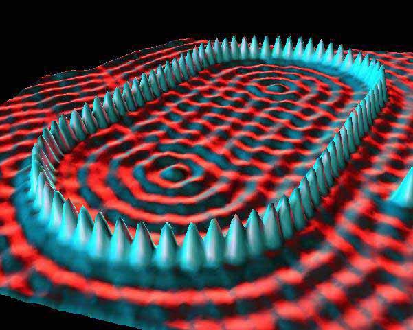
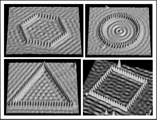
6 Quantum Correl 48 Fe adatoms on Cu(111) surface
7
8

 Electron diffraction")
9 Wave Nature of Electrons de Broglie s proposal: λ = h/p For electrons: (Å) = 150 E( ev ) Electron diffraction patterns


10 Noble Metal/W(111) Pyramidal Single-Atom Tips Traditional Ideal electron point source Electron Projection Microscopes (In-line holography ) M = D/d
.")
11 Melting Temperature of Nanopartcles 3D CdS nanocrystal 30 nm Goldstein, Echer, Alivisatos, Science 256, 1425 (1992).
12 Stability of Nanoparticles Traditional Picture of Nucleation and Growth n = 1 n = 2 n = 3 n = i n = i +1 Nucleation Growth Larger stable cluster Single atom Dimer Trimer Critical size Smallest stable island Unstable clusters G J. A. Venables et al., Rep. Prog. Phys. 47, 399 (1984). i+1
13 Magic Clusters 1. Magic clusters exhibit enhanced stability relative to clusters either slightly larger or smaller than the magic size. Thus, it is energetically unfavorable for magic clusters to grow in size by adding one or a few atoms. 2. Traditional nucleation theories: The cluster with a size of i*+1 is stable in a sense that they tend to grow larger by incorporating more atoms. That also means they have a higher free energy than that of clusters of larger sizes. They are not really stable! G n* Cluster size, n
14
15 Mass Analyzer B r qv = ½ mv 2 F = qvb = mv 2 /r m/q = ½ B 2 r 2 /V
16 Electronic Magic Numbers Clusters in which the number of valence electrons matches the spherical shell closing numbers are produced more abundantly. closed electronic shell The clusters are considered to be uniformly positively charged spheres filled with electrons.

")

17 Structural Magic Numbers Al 13 Mackay Icosahedra P = 1 20 fcc(111) faces P = 2 P = 3 N = 1 + Σ (10p 2 + 2)
18 Xe Magic Clusters
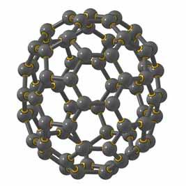
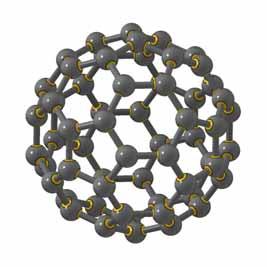
19 Fullerenes C 60 C 70
20 Reactivity of Nanoclusters
21 Catalytic Activities of Au Nanoparticles Au is usually viewed as an inert metal, but surprisingly it has been found that Au nanoparticles less than 3 5 nm in diameter are catalytically active for several chemical reactions. Nanotoday AUGUST 2007 Catalytic activities for CO oxidation at 273 K as a function of Au particle size

22 Ratio of surface atoms ratio (%) /d Diameter of particle d (nm)
23 The Structure of Surface Atoms on a surface of a solid have an environment that differs markedly from that of atoms in the bulk of the solid. They have fewer neighbors than do bulk atoms. On clean surface, two important structure changes can occur. 1.Bond-length contraction or relaxation 2.Reconstruction
24 Bond-length Contraction or Relaxation 1. In vacuum, virtually all surfaces relax. The spacing between the first and second atomic layers is significantly reduced from the spacing characterizing the bulk. 2. For a close-packed metal with a less close-packed surface, the interlayer spacing between the topmost and the second atomic layer is smaller than the bulk spacing. The perturbation caused by this surface relaxation propagates a few layers into the bulk. In fact, there is often a compensating expansion between the second and the third metal layer (on the order of 1%), accompanied by a small but detectable change in the next layer.
25 Relaxation Reconstruction Missing row reconstruction


-7 7, Ge(111)-c(2 8), Si(001)-(2")
, Pt(100), Au(100) Hexagonally")
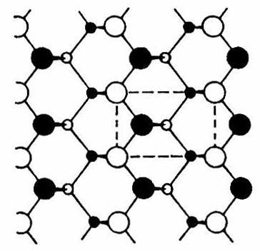
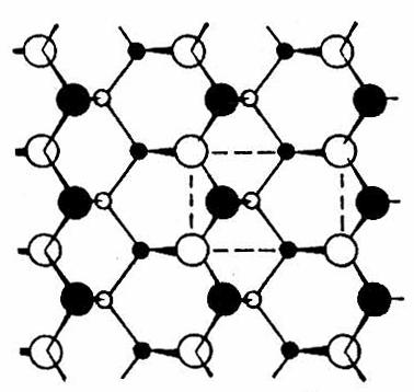
26 Reconstruction The surface can assume an atomic structure that differs fundamentally from the structure one would expect if the bulk structure terminated abruptly at the surface. For semiconductor surfaces, which are covalently bonded, the dangling bonds created at the surface cannot easily be satisfied except through more drastic rearrangements of these atoms. Example: Si(111)-7 7, Ge(111)-c(2 8), Si(001)-(2 1). Si(001) Many metal surfaces also reconstruct. Examples: Ir(100), Pt(100), Au(100) Hexagonally close-packed surface layer on square lattice. Ir(100)-(1x5) Pt(100)
27 GaAs(110)-(1x1) Top view Side view Sphere model (side view) Nonreconstructed Relaxed
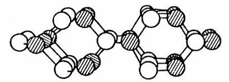
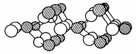
28 Si(111)-(2x1) Top view Side view Sphere model (side view) Nonreconstructed π Chain π Chain π Chain model
29 Lowest Energy Geometries proposed for the Si n (n 11) neutrals in the literature


30 Theoretical Model of Si 1000 Clusters Phys. Rev. B 57, 3799 (1998)

31 Theoretical Model for Metal-encapsulated Si n Clusters Phys. Rev. Lett. 87, (2001)


32 Miller Indices of a Plane
 Crystal")
33 Face-Centered Cubic (fcc) Crystal Surfaces
34 The Five Surface Net
35 Notation of Surface Structures 1. If the translation vectors of the surface, a and b, a = Ma, b = Nb, where a and b are the translation vectors of the ideal, unreconstructed surface. The nomenclature for this structure is (M N). If, in addition, the surface net is rotated with respect to the underlying substrate lattice by an angle degrees, the notation becomes (M N)R. If the surface net is best described using a centered, rather than a primitive net, this is indicated as c(m N). If the overlayer consists of an adsorbate, rather than simple reconstructed substrate atoms, this is also usually indicated. An arrangement of surface atoms identical to that in the bulk unit cell is called the substrate structure and is designated (1 1) (i.e. unreconstructed). 2. The surface unit-cell vectors a and b can be expressed in terms of the unit-cell vectors, a and b, obtained from the bulk projection. a = m 11 a + m 12 b, b = m 21 a + m 22 b, M = m m m m A surface structure that has a unit cell different from the bulk-projected substrate unit cell is often called a superlattice. (2 2) correspond to the matrix notation.
Spectroscopy at nanometer scale
 Spectroscopy at nanometer scale 1. Physics of the spectroscopies 2. Spectroscopies for the bulk materials 3. Experimental setups for the spectroscopies 4. Physics and Chemistry of nanomaterials Various
Spectroscopy at nanometer scale
 Spectroscopy at nanometer scale 1. Physics of the spectroscopies 2. Spectroscopies for the bulk materials 3. Experimental setups for the spectroscopies 4. Physics and Chemistry of nanomaterials Various
Bulk Structures of Crystals
 Bulk Structures of Crystals 7 crystal systems can be further subdivided into 32 crystal classes... see Simon Garrett, "Introduction to Surface Analysis CEM924": http://www.cem.msu.edu/~cem924sg/lecturenotes.html
2. Diffraction as a means to determine crystal structure
 Page 1 of 22 2. Diffraction as a means to determine crystal structure Recall de Broglie matter waves: 2 p h E = where p = 2m λ h 1 E = ( ) 2m λ hc E = hυ = ( photons) λ ( matter wave) He atoms: [E (ev)]
2. Diffraction as a means to determine crystal structure
 2. Diffraction as a means to determine crystal structure Recall de Broglie matter waves: He atoms: [E (ev)] 1/2 = 0.14 / (Å) E 1Å = 0.0196 ev Neutrons: [E (ev)] 1/2 = 0.28 / (Å) E 1Å = 0.0784 ev Electrons:
Surface Structure and Morphology 2D Crystallography
 Surface Structure and Morphology 2D Crystallography Selvage (or selvedge (it. cimosa)): Region in the solid in the vicinity of the mathematical surface Surface = Substrate (3D periodicity) + Selvage (few
STM spectroscopy (STS)
") STM spectroscopy (STS) di dv 4 e ( E ev, r) ( E ) M S F T F Basic concepts of STS. With the feedback circuit open the variation of the tunneling current due to the application of a small oscillating voltage
STM spectroscopy (STS) di dv 4 e ( E ev, r) ( E ) M S F T F Basic concepts of STS. With the feedback circuit open the variation of the tunneling current due to the application of a small oscillating voltage
disordered, ordered and coherent with the substrate, and ordered but incoherent with the substrate.
 5. Nomenclature of overlayer structures Thus far, we have been discussing an ideal surface, which is in effect the structure of the topmost substrate layer. The surface (selvedge) layers of the solid however
Scanning Tunneling Microscopy. how does STM work? the quantum mechanical picture example of images how can we understand what we see?
 Scanning Tunneling Microscopy how does STM work? the quantum mechanical picture example of images how can we understand what we see? Observation of adatom diffusion with a field ion microscope Scanning
2) Atom manipulation. Xe / Ni(110) Model: Experiment:
 Atom manipulation. Xe / Ni(110) Model: Experiment:") 2) Atom manipulation D. Eigler & E. Schweizer, Nature 344, 524 (1990) Xe / Ni(110) Model: Experiment: G.Meyer, et al. Applied Physics A 68, 125 (1999) First the tip is approached close to the adsorbate
2) Atom manipulation D. Eigler & E. Schweizer, Nature 344, 524 (1990) Xe / Ni(110) Model: Experiment: G.Meyer, et al. Applied Physics A 68, 125 (1999) First the tip is approached close to the adsorbate
Chapter 10: Modern Atomic Theory and the Periodic Table. How does atomic structure relate to the periodic table? 10.1 Electromagnetic Radiation
 Chapter 10: Modern Atomic Theory and the Periodic Table How does atomic structure relate to the periodic table? 10.1 Electromagnetic Radiation Electromagnetic (EM) radiation is a form of energy that exhibits
Surface physics, Bravais lattice
 Surface physics, Bravais lattice 1. Structure of the solid surface characterized by the (Bravais) lattice + space + point group lattice describes also the symmetry of the solid material vector directions
Lecture 6: Individual nanoparticles, nanocrystals and quantum dots
 Lecture 6: Individual nanoparticles, nanocrystals and quantum dots Definition of nanoparticle: Size definition arbitrary More interesting: definition based on change in physical properties. Size smaller
Chem 728 Introduction to Solid Surfaces
 Chem 728 Introduction to Solid Surfaces Solids: hard; fracture; not compressible; molecules close to each other Liquids: molecules mobile, but quite close to each other Gases: molecules very mobile; compressible
Surface Sensitivity & Surface Specificity
 Surface Sensitivity & Surface Specificity The problems of sensitivity and detection limits are common to all forms of spectroscopy. In its simplest form, the question of sensitivity boils down to whether
Basics of DFT applications to solids and surfaces
 Basics of DFT applications to solids and surfaces Peter Kratzer Physics Department, University Duisburg-Essen, Duisburg, Germany E-mail: Peter.Kratzer@uni-duisburg-essen.de Periodicity in real space and
Lecture 6 - Bonding in Crystals
 Lecture 6 onding in Crystals inding in Crystals (Kittel Ch. 3) inding of atoms to form crystals A crystal is a repeated array of atoms Why do they form? What are characteristic bonding mechanisms? How
Ionic Bonding. Example: Atomic Radius: Na (r = 0.192nm) Cl (r = 0.099nm) Ionic Radius : Na (r = 0.095nm) Cl (r = 0.181nm)
 Cl (r = 0.099nm) Ionic Radius : Na (r = 0.095nm) Cl (r = 0.181nm)") Ionic Bonding Ion: an atom or molecule that gains or loses electrons (acquires an electrical charge). Atoms form cations (+charge), when they lose electrons, or anions (- charge), when they gain electrons.
Ionic Bonding Ion: an atom or molecule that gains or loses electrons (acquires an electrical charge). Atoms form cations (+charge), when they lose electrons, or anions (- charge), when they gain electrons.
2. Surface geometric and electronic structure: a primer
 2. Surface geometric and electronic structure: a primer 2.1 Surface crystallography 2.1.1. Crystal structures - A crystal structure is made up of two basic elements: lattice + basis Basis: Lattice: simplest
Semiconductor physics I. The Crystal Structure of Solids
 Lecture 3 Semiconductor physics I The Crystal Structure of Solids 1 Semiconductor materials Types of solids Space lattices Atomic Bonding Imperfection and doping in SOLIDS 2 Semiconductor Semiconductors
Surface and Interface Science Physics 627; Chemistry 542. Lectures 3 Feb 1, Surface Structure
 Surface and Interface Science Physics 67; Chemistry 54 Lectures 3 Fe, 03 Surface Structure References: ) Zangwill, Pp. 8-3 ) Woodruff & Delchar, Chapter 3) Masel, Chapter 4) Ertl & Kuppers, 0-07 5) Luth,
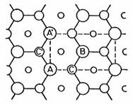
Structure of Surfaces
 Structure of Surfaces C Stepped surface Interference of two waves Bragg s law Path difference = AB+BC =2dsin ( =glancing angle) If, n =2dsin, constructive interference Ex) in a cubic lattice of unit cell
Nearly Free Electron Gas model - I
 Nearly Free Electron Gas model - I Contents 1 Free electron gas model summary 1 2 Electron effective mass 3 2.1 FEG model for sodium...................... 4 3 Nearly free electron model 5 3.1 Primitive
Lecture 8 January 24, 2013 GaAs crystal surfaces, n-p dopants Si
 Lecture 8 January 24, 2013 Ga crystal surfaces, n-p dopants Si Nature of the Chemical Bond with applications to catalysis, materials science, nanotechnology, surface science, bioinornic chemistry, and
Electronic Structure Theory for Periodic Systems: The Concepts. Christian Ratsch
 Electronic Structure Theory for Periodic Systems: The Concepts Christian Ratsch Institute for Pure and Applied Mathematics and Department of Mathematics, UCLA Motivation There are 10 20 atoms in 1 mm 3
Lecture 2. Unit Cells and Miller Indexes. Reading: (Cont d) Anderson 2 1.8,
 Anderson 2 1.8,") Lecture 2 Unit Cells and Miller Indexes Reading: (Cont d) Anderson 2 1.8, 2.1-2.7 Unit Cell Concept The crystal lattice consists of a periodic array of atoms. Unit Cell Concept A building block that can
Lecture 2 Unit Cells and Miller Indexes Reading: (Cont d) Anderson 2 1.8, 2.1-2.7 Unit Cell Concept The crystal lattice consists of a periodic array of atoms. Unit Cell Concept A building block that can
Experimental methods in physics. Local probe microscopies I
 Experimental methods in physics Local probe microscopies I Scanning tunnelling microscopy (STM) Jean-Marc Bonard Academic year 09-10 1. Scanning Tunneling Microscopy 1.1. Introduction Image of surface
Crystalline Solids have atoms arranged in an orderly repeating pattern. Amorphous Solids lack the order found in crystalline solids
 Ch 12: Solids and Modern Materials Learning goals and key skills: Classify solids base on bonding/intermolecular forces and understand how difference in bonding relates to physical properties Know the
1.4 Crystal structure
 1.4 Crystal structure (a) crystalline vs. (b) amorphous configurations short and long range order only short range order Abbildungen: S. Hunklinger, Festkörperphysik, Oldenbourg Verlag represenatives of
Theoretical and experimental factors affecting measurements of semiconductor mean inner potentials
 Journal of Physics: Conference Series Theoretical and experimental factors affecting measurements of semiconductor mean inner potentials Recent citations - Mapping Charge Distribution in Single PbS Core
Introduction to Solid State Physics or the study of physical properties of matter in a solid phase
 Introduction to Solid State Physics or the study of physical properties of matter in a solid phase Prof. Germar Hoffmann 1. Crystal Structures 2. Reciprocal Lattice 3. Crystal Binding and Elastic Constants
The Hamiltonian. 2.1 The Schrödinger Equation
 2 The Hamiltonian Any theoretical description has to start with the definition of the system under consideration and a determination of the fundamental interactions present in the system. This information
1. Introduction to Clusters
 1. Introduction to Clusters 1.1 The Field of Clusters Atomic clusters are aggregates of atoms containing from few to a few thousand atoms. Due to their small size, the properties of the clusters are, in
* motif: a single or repeated design or color
 Chapter 2. Structure A. Electronic structure vs. Geometric structure B. Clean surface vs. Adsorbate covered surface (substrate + overlayer) C. Adsorbate structure - how are the adsorbed molecules bound
CHAPTER 2. Atomic Structure And Bonding 2-1
 CHAPTER 2 Atomic Structure And Bonding 2-1 Structure of Atoms ATOM Basic Unit of an Element Diameter : 10 10 m. Neutrally Charged Nucleus Diameter : 10 14 m Accounts for almost all mass Positive Charge
Everything starts with atomic structure and bonding
 Everything starts with atomic structure and bonding not all energy values can be possessed by electrons; e- have discrete energy values we call energy levels or states. The energy values are quantized
Semiconductor Physics and Devices Chapter 3.
 Introduction to the Quantum Theory of Solids We applied quantum mechanics and Schrödinger s equation to determine the behavior of electrons in a potential. Important findings Semiconductor Physics and
Chemical Bonding Ionic Bonding. Unit 1 Chapter 2
 Chemical Bonding Ionic Bonding Unit 1 Chapter 2 Valence Electrons The electrons responsible for the chemical properties of atoms are those in the outer energy level. Valence electrons - The s and p electrons
Optical Properties of Solid from DFT
 Optical Properties of Solid from DFT 1 Prof.P. Ravindran, Department of Physics, Central University of Tamil Nadu, India & Center for Materials Science and Nanotechnology, University of Oslo, Norway http://folk.uio.no/ravi/cmt15
PBS: FROM SOLIDS TO CLUSTERS
 PBS: FROM SOLIDS TO CLUSTERS E. HOFFMANN AND P. ENTEL Theoretische Tieftemperaturphysik Gerhard-Mercator-Universität Duisburg, Lotharstraße 1 47048 Duisburg, Germany Semiconducting nanocrystallites like
Lecture 1 - Electrons, Photons and Phonons. September 4, 2002
 6.720J/3.43J - Integrated Microelectronic Devices - Fall 2002 Lecture 1-1 Lecture 1 - Electrons, Photons and Phonons Contents: September 4, 2002 1. Electronic structure of semiconductors 2. Electron statistics
Angle-Resolved Two-Photon Photoemission of Mott Insulator
 Angle-Resolved Two-Photon Photoemission of Mott Insulator Takami Tohyama Institute for Materials Research (IMR) Tohoku University, Sendai Collaborators IMR: H. Onodera, K. Tsutsui, S. Maekawa H. Onodera
Solids. properties & structure
 Solids properties & structure Determining Crystal Structure crystalline solids have a very regular geometric arrangement of their particles the arrangement of the particles and distances between them is
Supplementary Materials for
 advances.sciencemag.org/cgi/content/full/4/3/e1701373/dc1 Supplementary Materials for Atomically thin gallium layers from solid-melt exfoliation Vidya Kochat, Atanu Samanta, Yuan Zhang, Sanjit Bhowmick,
Surface Studies by Scanning Tunneling Microscopy
 Surface Studies by Scanning Tunneling Microscopy G. Binnig, H. Rohrer, Ch. Gerber, and E. Weibel IBM Zurich Research Laboratory, 8803 Ruschlikon-ZH, Switzerland (Received by Phys. Rev. Lett. on 30th April,
 lectures accompanying the book: Solid State Physics: An Introduction, by Philip ofmann (2nd edition 2015, ISBN-10: 3527412824, ISBN-13: 978-3527412822, Wiley-VC Berlin. www.philiphofmann.net 1 Bonds between
Concepts in Surface Physics
 M.-C. Desjonqueres D. Spanjaard Concepts in Surface Physics Second Edition With 257 Figures Springer 1. Introduction................................. 1 2. Thermodynamical and Statistical Properties of
STRUCTURAL AND MECHANICAL PROPERTIES OF AMORPHOUS SILICON: AB-INITIO AND CLASSICAL MOLECULAR DYNAMICS STUDY
 STRUCTURAL AND MECHANICAL PROPERTIES OF AMORPHOUS SILICON: AB-INITIO AND CLASSICAL MOLECULAR DYNAMICS STUDY S. Hara, T. Kumagai, S. Izumi and S. Sakai Department of mechanical engineering, University of
1 Review of semiconductor materials and physics
 Part One Devices 1 Review of semiconductor materials and physics 1.1 Executive summary Semiconductor devices are fabricated using specific materials that offer the desired physical properties. There are
Crystal Properties. MS415 Lec. 2. High performance, high current. ZnO. GaN
 Crystal Properties Crystal Lattices: Periodic arrangement of atoms Repeated unit cells (solid-state) Stuffing atoms into unit cells Determine mechanical & electrical properties High performance, high current
Chapter 2. Atomic Structure
 Chapter 2 Atomic Structure 2 6 (a) Aluminum foil used for storing food weighs about 0. g per square cm. How many atoms of aluminum are contained in one 6.25 cm 2 size of foil? (b) Using the densities and
Chapter 2. Atomic Packing
 Chapter 2. Atomic Packing Contents 2-1. Packing of directional bonding atoms 2-2. Packing of indirectional bonding in same size atoms 2-3. Packing of indirectional bonding in different size atoms 2-4.
The first three categories are considered a bottom-up approach while lithography is a topdown
 Nanowires and Nanorods One-dimensional structures have been called in different ways: nanowires, nanorod, fibers of fibrils, whiskers, etc. The common characteristic of these structures is that all they
Monte Carlo simulations of alloy segregation in PtAg octahedral nanoparticles
 Monte Carlo simulations of alloy segregation in PtAg octahedral nanoparticles Louis C. Jones 6/8/12 Abstract Simulations were carried out to investigate phase segregation of insoluble alloy nanoparticles
Optical Properties of Semiconductors. Prof.P. Ravindran, Department of Physics, Central University of Tamil Nadu, India
 Optical Properties of Semiconductors 1 Prof.P. Ravindran, Department of Physics, Central University of Tamil Nadu, India http://folk.uio.no/ravi/semi2013 Light Matter Interaction Response to external electric
EE495/695 Introduction to Semiconductors I. Y. Baghzouz ECE Department UNLV
 EE495/695 Introduction to Semiconductors I Y. Baghzouz ECE Department UNLV Introduction Solar cells have always been aligned closely with other electronic devices. We will cover the basic aspects of semiconductor
The Solid State. Phase diagrams Crystals and symmetry Unit cells and packing Types of solid
 The Solid State Phase diagrams Crystals and symmetry Unit cells and packing Types of solid Learning objectives Apply phase diagrams to prediction of phase behaviour Describe distinguishing features of
Lecture 3: Heterostructures, Quasielectric Fields, and Quantum Structures
 Lecture 3: Heterostructures, Quasielectric Fields, and Quantum Structures MSE 6001, Semiconductor Materials Lectures Fall 2006 3 Semiconductor Heterostructures A semiconductor crystal made out of more
EECS143 Microfabrication Technology
 EECS143 Microfabrication Technology Professor Ali Javey Introduction to Materials Lecture 1 Evolution of Devices Yesterday s Transistor (1947) Today s Transistor (2006) Why Semiconductors? Conductors e.g
Materials 218/UCSB: Class III Cohesion in solids van der Waals, ionic, covalent, metallic
 Materials 218/UCSB: Class III Cohesion in solids van der Waals, ionic, covalent, metallic Ram Seshadri (seshadri@mrl.ucsb.edu) Introduction There are four forces in nature. The strong and the weak interactions
Spectroscopies for Unoccupied States = Electrons
 Spectroscopies for Unoccupied States = Electrons Photoemission 1 Hole Inverse Photoemission 1 Electron Tunneling Spectroscopy 1 Electron/Hole Emission 1 Hole Absorption Will be discussed with core levels
Formation mechanism and Coulomb blockade effect in self-assembled gold quantum dots
 Formation mechanism and Coulomb blockade effect in self-assembled gold quantum dots S. F. Hu a) National Nano Device Laboratories, Hsinchu 300, Taiwan R. L. Yeh and R. S. Liu Department of Chemistry, National
Lecture contents. Stress and strain Deformation potential. NNSE 618 Lecture #23
 1 Lecture contents Stress and strain Deformation potential Few concepts from linear elasticity theory : Stress and Strain 6 independent components 2 Stress = force/area ( 3x3 symmetric tensor! ) ij ji
Physics and Material Science of Semiconductor Nanostructures
 Physics and Material Science of Semiconductor Nanostructures PHYS 570P Prof. Oana Malis Email: omalis@purdue.edu Course website: http://www.physics.purdue.edu/academic_programs/courses/phys570p/ 1 Introduction
2008 Brooks/Cole 2. Frequency (Hz)
") Electromagnetic Radiation and Matter Oscillating electric and magnetic fields. Magnetic field Electric field Chapter 7: Electron Configurations and the Periodic Table Traveling wave moves through space
Electromagnetic Radiation and Matter Oscillating electric and magnetic fields. Magnetic field Electric field Chapter 7: Electron Configurations and the Periodic Table Traveling wave moves through space
Photon Interaction. Spectroscopy
 Photon Interaction Incident photon interacts with electrons Core and Valence Cross Sections Photon is Adsorbed Elastic Scattered Inelastic Scattered Electron is Emitted Excitated Dexcitated Stöhr, NEXAPS
Supplementary Figure 1 Experimental setup for crystal growth. Schematic drawing of the experimental setup for C 8 -BTBT crystal growth.
 Supplementary Figure 1 Experimental setup for crystal growth. Schematic drawing of the experimental setup for C 8 -BTBT crystal growth. Supplementary Figure 2 AFM study of the C 8 -BTBT crystal growth
Electronic Properties of Ultimate Nanowires. F. J. Himpsel, S. C. Erwin, I. Barke,
 Electronic Properties of Ultimate Nanowires F. J. Himpsel, S. C. Erwin, I. Barke, Nanostructures with Atomic Precision Single-Atom Wire, Single Wave Function Ultimate Limits of Electronics, Data Storage
Electrons are shared in covalent bonds between atoms of Si. A bound electron has the lowest energy state.
 Photovoltaics Basic Steps the generation of light-generated carriers; the collection of the light-generated carriers to generate a current; the generation of a large voltage across the solar cell; and
Nano-optics. Topics: How do we image things on the nanoscale? How do we use nanofabrication for new optical devices? COSMOS 2006 Lecture 1
 Nano-optics Topics: How do we image things on the nanoscale? How do we use nanofabrication for new optical devices? Wave Optics 1. Electromagnetic wave x Ex λ Direction of Propagation y z z plane wave
Ch. 7 The Quantum Mechanical Atom. Brady & Senese, 5th Ed.
 Ch. 7 The Quantum Mechanical Atom Brady & Senese, 5th Ed. Index 7.1. Electromagnetic radiation provides the clue to the electronic structures of atoms 7.2. Atomic line spectra are evidence that electrons
For preparing Sn adatoms on the Si(111)-(7 7) surface, we used a filamenttype
-(7 7) surface, we used a filamenttype") Supplementary Methods 1 1.1 Germanium For preparing Ge adatoms on the Si(111)-(7 7) surface, we used a filamenttype source which wrapped a grain of Ge (Purity: 99.999 %). After preparing the clean Si(111)-(7
Supplementary Methods 1 1.1 Germanium For preparing Ge adatoms on the Si(111)-(7 7) surface, we used a filamenttype source which wrapped a grain of Ge (Purity: 99.999 %). After preparing the clean Si(111)-(7
PART 1 Introduction to Theory of Solids
 Elsevier UK Job code: MIOC Ch01-I044647 9-3-2007 3:03p.m. Page:1 Trim:165 240MM TS: Integra, India PART 1 Introduction to Theory of Solids Elsevier UK Job code: MIOC Ch01-I044647 9-3-2007 3:03p.m. Page:2
Electron Energy, E E = 0. Free electron. 3s Band 2p Band Overlapping energy bands. 3p 3s 2p 2s. 2s Band. Electrons. 1s ATOM SOLID.
 Electron Energy, E Free electron Vacuum level 3p 3s 2p 2s 2s Band 3s Band 2p Band Overlapping energy bands Electrons E = 0 1s ATOM 1s SOLID In a metal the various energy bands overlap to give a single
EE143 Fall 2016 Microfabrication Technologies. Evolution of Devices
 EE143 Fall 2016 Microfabrication Technologies Prof. Ming C. Wu wu@eecs.berkeley.edu 511 Sutardja Dai Hall (SDH) 1-1 Evolution of Devices Yesterday s Transistor (1947) Today s Transistor (2006) 1-2 1 Why
Lecture 2: Bonding in solids
 Lecture 2: Bonding in solids Electronegativity Van Arkel-Ketalaar Triangles Atomic and ionic radii Band theory of solids Molecules vs. solids Band structures Analysis of chemical bonds in Reciprocal space
Atomic Structure & Interatomic Bonding
 Atomic Structure & Interatomic Bonding Chapter Outline Review of Atomic Structure Atomic Bonding Atomic Structure Atoms are the smallest structural units of all solids, liquids & gases. Atom: The smallest
CLUSTERS: CHEMISTRY AND PHYSICS IN A FINITE WORLD. TONY STACE University of Nottingham
 CLUSTERS: CHEMISTRY AND PHYSICS IN A FINITE WORLD TONY STACE University of Nottingham Clusters: Small collections (~ 1000) of atoms and/or molecules that are typically studied in the gas phase. These could
Metal Oxides Surfaces
 Chapter 2 Metal xides Surfaces 2.1 Cobalt xides 1. Co Co (cobalt monoxide) with rocksalt structure (NaCl structure) consists of two interpenetrating fcc sublattices of Co 2+ and 2. These two sublattices
- Light has properties of WAVES such as DIFFRACTION (it bends around small obstructions).
.") 170 LIGHT wavelength Diffraction frequency = wavelengths / time = - Light has properties of WAVES such as DIFFRACTION (it bends around small obstructions). - Einstein noted that viewing light as a particle
170 LIGHT wavelength Diffraction frequency = wavelengths / time = - Light has properties of WAVES such as DIFFRACTION (it bends around small obstructions). - Einstein noted that viewing light as a particle
Structure analysis: Electron diffraction LEED TEM RHEED
 Structure analysis: Electron diffraction LEED: Low Energy Electron Diffraction SPA-LEED: Spot Profile Analysis Low Energy Electron diffraction RHEED: Reflection High Energy Electron Diffraction TEM: Transmission
Energy bands in solids. Some pictures are taken from Ashcroft and Mermin from Kittel from Mizutani and from several sources on the web.
 Energy bands in solids Some pictures are taken from Ashcroft and Mermin from Kittel from Mizutani and from several sources on the web. we are starting to remind p E = = mv 1 2 = k mv = 2 2 k 2m 2 Some
- Atomic line spectra are UNIQUE to each element. They're like atomic "fingerprints".
 - Atomic line spectra are UNIQUE to each element. They're like atomic "fingerprints". - Problem was that the current model of the atom completely failed to explain why atoms emitted these lines. An orbit
Bonding in solids The interaction of electrons in neighboring atoms of a solid serves the very important function of holding the crystal together.
 Bonding in solids The interaction of electrons in neighboring atoms of a solid serves the very important function of holding the crystal together. For example Nacl In the Nacl lattice, each Na atom is
Epitaxial Growth of Mn on Si(111)
") 105 Chapter 7 Epitaxial Growth of Mn on Si(111) 7.1 Introduction There are a few reports and experiments concerning the adsoption of Mn on Si(111), where film growth with and without a Bi surfactant layer
105 Chapter 7 Epitaxial Growth of Mn on Si(111) 7.1 Introduction There are a few reports and experiments concerning the adsoption of Mn on Si(111), where film growth with and without a Bi surfactant layer
Direct and Indirect Semiconductor
 Direct and Indirect Semiconductor Allowed values of energy can be plotted vs. the propagation constant, k. Since the periodicity of most lattices is different in various direction, the E-k diagram must
Survey of structural and electronic properties of C60 on close-packed metal surfaces
 Hong Kong Baptist University From the SelectedWorks of Professor Michel Andre Van Hove 2012 Survey of structural and electronic properties of C60 on close-packed metal surfaces Xing-Qiang Shi, Department
Ram Seshadri MRL 2031, x6129, These notes complement chapter 6 of Anderson, Leaver, Leevers and Rawlings
 Crystals, packings etc. Ram Seshadri MRL 2031, x6129, seshadri@mrl.ucsb.edu These notes complement chapter 6 of Anderson, Leaver, Leevers and Rawlings The unit cell and its propagation Materials usually
GaAs equilibrium crystal shape from first principles
 PHYSICAL REVIEW B VOLUME 54, NUMBER 12 GaAs equilibrium crystal shape from first principles 15 SEPTEMBER 1996-II N. Moll,* A. Kley, E. Pehlke, and M. Scheffler Fritz-Haber-Institut der Max-Planck-Gesellschaft,
Energy band of manipulated atomic structures on an insulator substrate
 Energy band of manipulated atomic structures on an insulator substrate Toshishige Yamada and Yoshihisa Yamamoto ERATO Quantum Fluctuation Project, Edward L. Ginzton Laboratory, Stanford University, Stanford,
Chapter 4: Bonding in Solids and Electronic Properties. Free electron theory
 Chapter 4: Bonding in Solids and Electronic Properties Free electron theory Consider free electrons in a metal an electron gas. regards a metal as a box in which electrons are free to move. assumes nuclei
SUPPLEMENTARY INFORMATION
 In the format provided by the authors and unedited. Intrinsically patterned two-dimensional materials for selective adsorption of molecules and nanoclusters X. Lin 1,, J. C. Lu 1,, Y. Shao 1,, Y. Y. Zhang
Introductory Nanotechnology ~ Basic Condensed Matter Physics ~
 Introductory Nanotechnology ~ Basic Condensed Matter Physics ~ Atsufumi Hirohata Department of Electronics Go into Nano-Scale Lateral Size [m] 10-3 10-6 Micron-scale Sub-Micron-scale Nano-scale Human hair
Lecture 8 January 28, Silicon crystal surfaces
 Lecture 8 January 28, 203 Nature of the Chemical Bond with applications to catalysis, materials science, nanotechnology, surface science, bioinorganic chemistry, and energy Course number: Ch20a Hours:
Physics 211B : Problem Set #0
 Physics 211B : Problem Set #0 These problems provide a cross section of the sort of exercises I would have assigned had I taught 211A. Please take a look at all the problems, and turn in problems 1, 4,
Chapter 3: Elements and Compounds. 3.1 Elements
 Chapter 3: Elements and Compounds 3.1 Elements An element is a fundamental substance that cannot be broken down by chemical or physical methods to simpler substances. The 118 known elements are nature
Probing Matter: Diffraction, Spectroscopy and Photoemission
 Probing Matter: Diffraction, Spectroscopy and Photoemission Anders Nilsson Stanford Synchrotron Radiation Laboratory Why X-rays? VUV? What can we hope to learn? 1 Photon Interaction Incident photon interacts
Institut des NanoSciences de Paris
 CNRS / Photothèque Cyril Frésillon Institut des NanoSciences de Paris Polarity in low dimensions: MgO nano-ribbons on Au(111) J. Goniakowski, C. Noguera Institut des Nanosciences de Paris, CNRS & Université
sin[( t 2 Home Problem Set #1 Due : September 10 (Wed), 2008
, 2008") Home Problem Set #1 Due : September 10 (Wed), 008 1. Answer the following questions related to the wave-particle duality. (a) When an electron (mass m) is moving with the velocity of υ, what is the wave
Home Problem Set #1 Due : September 10 (Wed), 008 1. Answer the following questions related to the wave-particle duality. (a) When an electron (mass m) is moving with the velocity of υ, what is the wave
Name: (a) What core levels are responsible for the three photoelectron peaks in Fig. 1?
 What core levels are responsible for the three photoelectron peaks in Fig. 1?") Physics 243A--Surface Physics of Materials: Spectroscopy Final Examination December 16, 2014 (3 problems, 100 points total, open book, open notes and handouts) Name: [1] (50 points), including Figures
Physics 243A--Surface Physics of Materials: Spectroscopy Final Examination December 16, 2014 (3 problems, 100 points total, open book, open notes and handouts) Name: [1] (50 points), including Figures