Structure of Surfaces
|
|
|
- Kathlyn Howard
- 5 years ago
- Views:
Transcription
1 Structure of Surfaces
2 C
3
4 Stepped surface

5 Interference of two waves
 in a cubic lattice of unit cell a sin = /2d = (h 2 +k 2 +l 2 ) ½ /2a")
6 Bragg s law Path difference = AB+BC =2dsin ( =glancing angle) If, n =2dsin, constructive interference Ex) in a cubic lattice of unit cell a sin = /2d = (h 2 +k 2 +l 2 ) ½ /2a determination of a
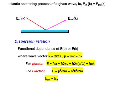
7 de Broglie relation in 1924 Any particle traveling with a linear momentum p has a wavelength Matter wave: p = mv = h/λ
8
9
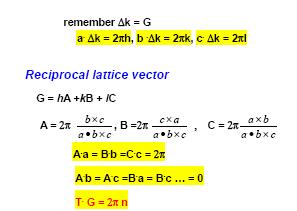
10 Δk = 2π/d n = G
11
12
13 radius 00
14
15
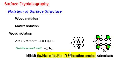
16 a b
17 Park & Madden : Matrix- notation b 1 = m 11 a 1 + m 12 a 2 b 2 = m 21 a 1 + m 22 a 2 ( b = M a M = m 11 m 12 ) m 21 m 22 - Area of unit cell A = l a 1 a 2 l B = l b 1 b 2 l - B = (m 11 m 22 m 12 m 21 ) A = A det M
18 Substrate lattice a 1, a 2 Surface structure b 1, b 2 b = M a Then, b 1 = m 11 a 1 + m 12 a 2 & b 2 = m 21 a 1 + m 22 a 2 In a similar way, reciprocal lattice b* can be expressed in terms of reciprocal lattice a*. b 1 * = m 11 * a 1 * + m 12 * a 2 * b 2 * = m 21 * a 1 * + m 22 * a 2 * M* : inverse transposed matrix of M ~ M* = M -1 ~ and M = M* -1
19 A = a 11 a 12 a 21 a 22 -a 21 a 11 A-1 = 1/detA a 22 -a 12 A T = a 11 a 21 a 12 a 22 (A T ) -1 =1/det A a 22 -a 21 -a 12 a 11
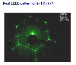
20 i.e. m 11 = 1/(det M*) m 22 * m 12 = -1/(det M*) m 21 * m 21 = -1/(det M*) m 12 * m 22 = 1/(det M*) m 11 * From reciprocal lattice (i.e. LEED pattern), real surface lattice can be induced.
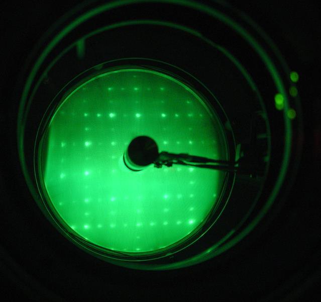
21 Interference conditions and the Ewald construction 2 /a k 2 1 k a 2 1 Scattering angle
22
23
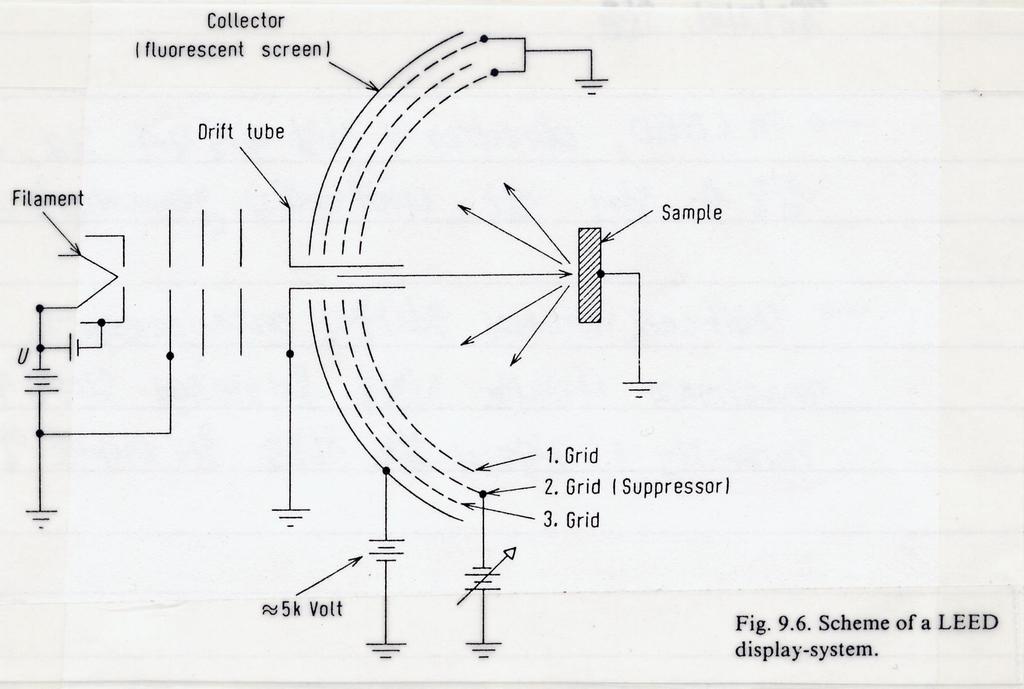
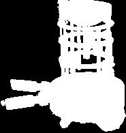
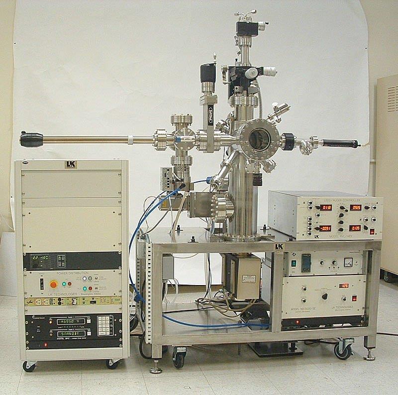
24 LEED (low energy electron diffraction) -display type (1) Heated cathode emits electrons (2) Electrons are collimated by a lens system and finally leave the drift tube with energy U ( ev). (3) Drift tube and sample: grounded. - electrons go through the field free space to sample. (4) Electron beam diameter= 1 mm at crystal surface due to finite size of cathode. - energy spread of electrons = ~1eV due to thermal energy distribution - emission current = ~ 1 A vary with energy U
25 (5) back-scattered electrons pass the 1 st grid which is grounded: Scattered electrons are not electrostatically deflected in the field free region between sample and grid. (6) 2 nd grid is at the negative potential slightly lower than the primary electron energy: prohibits the passage of inelastically scattered electrons. (7) Addition of extra grid between the 2 nd grid and the fluorescent screen to improve the LEED pattern. (Since the high voltage of the screen induces the field inhomogeneity in the 2 nd grid mesh) (8) 4 th grid improves the resolution. (9) Elastically scattered electrons are accelerated by positive potential of a few kv to fluorescent screen. (10) diffraction spots at the positions of interference maxima. (11) Observation of LEED pattern through the window of vacuum chamber or taking a picture of the pattern.
26
27 (1) Periodicity along the surface normal is lost in 2D arrangement of atoms: no constructive interference of scattered waves. (2) Reciprocal lattice: distance 1/(distance of real space) in z-direction, c* reciprocal lattice has a set of infinitely long rods normal to the plane of atoms. a i * a j * = 2 ij ij = 1, i=j or =0, i j a i *, a j * : unit mesh of the reciprocal lattice a i, a j : unit mesh of the real lattice E = (h 2 /2m)k 2, k = 2 / (3) In 2D, Ewald sphere construction : reciprocal rods are labeled with only 2 indices h, k General reciprocal lattice vector G g hk = h a 1 * + k a 2 *
28 (4) Diffraction occurs everywhere the Ewald sphere cuts a reciprocal lattice rod & the diffracted beam is labeled with (h, k) of the rod. k ll = k 0ll + g hk ( K ll = G hk ) k = k 0 (energy conservation) (5) In 1D k ll = 2 / cos (90- ) k 0ll = 2 / sin o 2 / (sin - sin o ) = 2 h/a a (sin - sin o ) = h k 0 o k
29 (6) In LEED, scattered beam k direction comes from the diffraction spots. (intersection of scattered beam & fluorescent screen) Observed LEED diffraction pattern = direct description of surface reciprocal lattice. (7) As k (1/ ), increase in the radius of Ewald sphere. More diffraction spots which move in continuously toward (0,0) spot. (8) (0,0) spot: no change in position with E (since direct reflection of primary beam at surface without diffraction.)
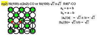
30 Ex) fcc(100) surface LEED Pattern (01) (11) a 2 a 2 * (00) (10) a 1 adsorbate a 1 * b 2 b 2 * b 1 * b 1 b 1 = 2 a 1 b 2 = 2a 2 b 1 * = ½ a 1 = ½ a 1 * b 2 * = ½ a 2 = ½ a 2 * b* = ½ 0 a* 0 ½ Det (M*) = ¼ m 11 =1/(¼ ) x ½ = 2 m 22 =1/(¼ ) x ½ = 2
31 Interpretation of LEED pattern (1)Diffraction pattern (2) c(2x2) a 2 * b 2 * b 1 * a 1 * b 2 a 1 a 2 b1 b 1 * = ½ a 1 * + ½ a 2 * b 2 * = -½ a 1 * + ½ a 2 * b 1 = a 1 + a 2 b 2 = -a 1 + a 2 M*= ½ ½ -½ ½ det M* = ½ Then, m 11 = 2x1/2 =1, m 12 = -2 x (-1/2)=1 m 21 = -2x1/2 =-1, m 22 = 2 x (1/2)=1
32
33
34
35 Electron Diffraction and Surface Defect Structures (1)Perfect crystal with a perfect instrument - infinitely sharp spots with zero intensity between (2) Finite instrumental limitations - finite width of spots & possibly some background (3) Deviations from periodicity by defects in structure or varying composition - alter spot shape & background dramatically (4) Inelastic scattering - may change the pattern
36 Kinds of surface defects (1)zero-dimensional: point defects due to contamination atoms, missing substrate atoms, or atoms which are displaced temporarily or permanently out of their regular lattice positions (2)1D defects: atomic steps or superstructure domain boundaries (3)2D defects: facets or amorphous top layers
37 <Kinds of information in the diffraction pattern> (1) Spot separation: always reciprocal to a frequently occurring distance - maybe regular atomic distance due to substrate structure or to superstructure or it may be the average distance between groups of atoms (2) Spot shape: reflects the range of coherent or in-phase scattering - If this range is smaller than the coherent range due to instrumental limitation, it represents the average size of regular atomic position (ex) domain size of superstructure or terrace width of step structure (3) Background - Contains information on the # and correlations of point defects - even in the case of ideal lattice, background intensity due to inelastic process - difficult to distinguish from the elastic process
38 Vibrations at surfaces - In each solid, the atoms are oscillating around their equilibrium positions due to their thermal energy. -Phonon: energy quantum of a lattice vibration (a) considered as a quasi particle with energy h (b) surface phonons influence specific heat, surface free energy, mean square displacement of surface atoms, thermal expansion (c) phonons may be localized or propagate parallel to the surface -Variation of LEED intensities : I of diffraction spots gradually decrease with increasing T & finally disappear in the background which become continuously brighter ln I -T
39 Debye spectrum D LEED intensity I = I 0 e -2W, 2W = 12h 2 /mk (cos / ) 2 T/ D 2 e- 2W = Debye-Waller factor Debye frequency: maximum possible frequency in Debye spectrum D = h /k : Debye temperature m= mass of atoms k=boltzman s constant = scattering angle of electrons = wavelength D = Debye temp.
40 Mean square displacement <u 2 > = 3h 2 /(4 2 m k) (T/ D2 ) ln I vs. T determines D or <u 2 >

41 (1) Energy dependence D vs. E p -With increase in Ep, D approaches the D bulk -Since increase in penetration depth with increase in Ep, increase in the detected volume -i.e. D surface << D bulk
 <u 2 > in surface normal > <u 2 > in surface parallel -Calculations")
42 (2) (00) beam intensity vs. T with variation of -Decrease in D when =0 compared to with =70 (grazing incidence) <u 2 > in surface normal > <u 2 > in surface parallel -Calculations for fcc(100) surfaces of (Cu, Ag, Au, Al, Pb, Ni, Pd, Pt) <u 2 > surface ~ 2.0 <u 2 >bulk <u 2 > // surface ~ <u 2 >bulk
M2 TP. Low-Energy Electron Diffraction (LEED)
") M2 TP Low-Energy Electron Diffraction (LEED) Guide for report preparation I. Introduction: Elastic scattering or diffraction of electrons is the standard technique in surface science for obtaining structural
M2 TP Low-Energy Electron Diffraction (LEED) Guide for report preparation I. Introduction: Elastic scattering or diffraction of electrons is the standard technique in surface science for obtaining structural
disordered, ordered and coherent with the substrate, and ordered but incoherent with the substrate.
 5. Nomenclature of overlayer structures Thus far, we have been discussing an ideal surface, which is in effect the structure of the topmost substrate layer. The surface (selvedge) layers of the solid however
Surface Sensitivity & Surface Specificity
 Surface Sensitivity & Surface Specificity The problems of sensitivity and detection limits are common to all forms of spectroscopy. In its simplest form, the question of sensitivity boils down to whether
Structure analysis: Electron diffraction LEED TEM RHEED
 Structure analysis: Electron diffraction LEED: Low Energy Electron Diffraction SPA-LEED: Spot Profile Analysis Low Energy Electron diffraction RHEED: Reflection High Energy Electron Diffraction TEM: Transmission
 Name : Roll No. :.... Invigilator s Signature :.. CS/B.Tech (NEW)/SEM-2/PH-201/2013 2013 PHYSICS - I Time Allotted : 3 Hours Full Marks : 70 The figures in the margin indicate full marks. Candidates are
Class 29: Reciprocal Space 3: Ewald sphere, Simple Cubic, FCC and BCC in Reciprocal Space
 Class 29: Reciprocal Space 3: Ewald sphere, Simple Cubic, FCC and BCC in Reciprocal Space We have seen that diffraction occurs when, in reciprocal space, Let us now plot this information. Let us designate
CHAPTER 3. SURFACE STRUCTURE 84
 CHAPTER 3. SURFACE STRUCTURE 84 3.3.1.2 Deviation from the Ideal Case 1. Lattice of finite size How does the interference function look like after summing up I G 2? Consider: M 1 x m = x m m=0 m=0 m=m
Crystal Structure and Electron Diffraction
 Crystal Structure and Electron Diffraction References: Kittel C.: Introduction to Solid State Physics, 8 th ed. Wiley 005 University of Michigan, PHY441-44 (Advanced Physics Laboratory Experiments, Electron
Electron Diffraction
 Electron iffraction o moving electrons display wave nature? To answer this question you will direct a beam of electrons through a thin layer of carbon and analyze the resulting pattern. Theory Louis de
High-Resolution. Transmission. Electron Microscopy
 Part 4 High-Resolution Transmission Electron Microscopy 186 Significance high-resolution transmission electron microscopy (HRTEM): resolve object details smaller than 1nm (10 9 m) image the interior of
CHEM-E5225 :Electron Microscopy. Diffraction 1
 CHEM-E5225 :Electron Microscopy Diffraction 1 2018-10-15 Yanling Ge Text book: Transmission electron microscopy by David B Williams & C. Barry Carter. 2009, Springer Outline Diffraction in TEM Thinking
An Introduction to Diffraction and Scattering. School of Chemistry The University of Sydney
 An Introduction to Diffraction and Scattering Brendan J. Kennedy School of Chemistry The University of Sydney 1) Strong forces 2) Weak forces Types of Forces 3) Electromagnetic forces 4) Gravity Types
Physics with Neutrons I, WS 2015/2016. Lecture 11, MLZ is a cooperation between:
 Physics with Neutrons I, WS 2015/2016 Lecture 11, 11.1.2016 MLZ is a cooperation between: Organization Exam (after winter term) Registration: via TUM-Online between 16.11.2015 15.1.2015 Email: sebastian.muehlbauer@frm2.tum.de
Particles and Waves Particles Waves
 Particles and Waves Particles Discrete and occupy space Exist in only one location at a time Position and velocity can be determined with infinite accuracy Interact by collisions, scattering. Waves Extended,
Surface Structure and Morphology 2D Crystallography
 Surface Structure and Morphology 2D Crystallography Selvage (or selvedge (it. cimosa)): Region in the solid in the vicinity of the mathematical surface Surface = Substrate (3D periodicity) + Selvage (few
Ultrafast Electron Crystallography: Principles and Dynamics
 15 Chapter 2 Ultrafast Electron Crystallography: Principles and Dynamics Part of this chapter was adapted from D.-S. Yang, N. Gedik, A. H. Zewail, J. Phys. Chem. C 111, 4889 (2007). 16 Introduction The
Electron Microscopy I
 Characterization of Catalysts and Surfaces Characterization Techniques in Heterogeneous Catalysis Electron Microscopy I Introduction Properties of electrons Electron-matter interactions and their applications
V 11: Electron Diffraction
 Martin-Luther-University Halle-Wittenberg Institute of Physics Advanced Practical Lab Course V 11: Electron Diffraction An electron beam conditioned by an electron optical system is diffracted by a polycrystalline,
4. Other diffraction techniques
 4. Other diffraction techniques 4.1 Reflection High Energy Electron Diffraction (RHEED) Setup: - Grazing-incidence high energy electron beam (3-5 kev: MEED,
Transmission Electron Microscopy
 L. Reimer H. Kohl Transmission Electron Microscopy Physics of Image Formation Fifth Edition el Springer Contents 1 Introduction... 1 1.1 Transmission Electron Microscopy... 1 1.1.1 Conventional Transmission
The University of Hong Kong Department of Physics
 The University of Hong Kong Department of Physics Physics Laboratory PHYS3551 Introductory Solid State Physics Experiment No. 3551-2: Electron and Optical Diffraction Name: University No: This experiment
Chapter Six: X-Rays. 6.1 Discovery of X-rays
 Chapter Six: X-Rays 6.1 Discovery of X-rays In late 1895, a German physicist, W. C. Roentgen was working with a cathode ray tube in his laboratory. He was working with tubes similar to our fluorescent
SOLID STATE 18. Reciprocal Space
 SOLID STATE 8 Reciprocal Space Wave vectors and the concept of K-space can simplify the explanation of several properties of the solid state. They will be introduced to provide more information on diffraction
Elastic and Inelastic Scattering in Electron Diffraction and Imaging
 Elastic and Inelastic Scattering in Electron Diffraction and Imaging Contents Introduction Symbols and definitions Part A Diffraction and imaging of elastically scattered electrons Chapter 1. Basic kinematical
Experiment 12 ELECTRON DIFFRACTION. Diffraction by Graphite 1. Diffraction by Aluminum 3. The Electron Diffraction Apparatus 5
 1-i Experiment 1 ELECTRON DIFFRACTION Introduction 1 Diffraction by Graphite 1 Diffraction by Aluminum 3 The Electron Diffraction Apparatus 5 Procedure and Analysis 6 References 7 Prelab Problems 8 Appendix
Quantum Condensed Matter Physics Lecture 5
 Quantum Condensed Matter Physics Lecture 5 detector sample X-ray source monochromator David Ritchie http://www.sp.phy.cam.ac.uk/drp2/home QCMP Lent/Easter 2019 5.1 Quantum Condensed Matter Physics 1. Classical
Wave Properties of Particles Louis debroglie:
 Wave Properties of Particles Louis debroglie: If light is both a wave and a particle, why not electrons? In 194 Louis de Broglie suggested in his doctoral dissertation that there is a wave connected with
1 P a g e h t t p s : / / w w w. c i e n o t e s. c o m / Physics (A-level)
") 1 P a g e h t t p s : / / w w w. c i e n o t e s. c o m / Physics (A-level) Electromagnetic induction (Chapter 23): For a straight wire, the induced current or e.m.f. depends on: The magnitude of the magnetic
1 P a g e h t t p s : / / w w w. c i e n o t e s. c o m / Physics (A-level) Electromagnetic induction (Chapter 23): For a straight wire, the induced current or e.m.f. depends on: The magnitude of the magnetic
A NEW LEED INSTRUMENT FOR QUANTITATIVE SPOT PROFILE ANALYSIS
 A NEW LEED INSTRUMENT FOR QUANTITATIVE SPOT PROFILE ANALYSIS U. Scheithauer, G. Meyer and M. Henzler Institut für Festkörperphysik, Universität Hannover, Appelstr. 2 Keywords LEED, spot profile analysis,
Revision Guide. Chapter 7 Quantum Behaviour
 Revision Guide Chapter 7 Quantum Behaviour Contents CONTENTS... 2 REVISION CHECKLIST... 3 REVISION NOTES... 4 QUANTUM BEHAVIOUR... 4 Random arrival of photons... 4 Photoelectric effect... 5 PHASE AN PHASORS...
In a particular investigation the atomic spacing of the crystal is m and the electrons are accelerated through 3000 V.
 1 Crystal structure can be investigated using the diffraction of an electron beam. A typical diffraction pattern is shown. In a particular investigation the atomic spacing of the crystal is 2.3 10 11 m
 Name : Roll No. :.. Invigilator s Signature :.. CS/B.Tech/SEM-2/PH-201/2010 2010 ENGINEERING PHYSICS Time Allotted : 3 Hours Full Marks : 70 The figures in the margin indicate full marks. Candidates are
Chapter 10: Wave Properties of Particles
 Chapter 10: Wave Properties of Particles Particles such as electrons may demonstrate wave properties under certain conditions. The electron microscope uses these properties to produce magnified images
2. Diffraction as a means to determine crystal structure
 2. Diffraction as a means to determine crystal structure Recall de Broglie matter waves: He atoms: [E (ev)] 1/2 = 0.14 / (Å) E 1Å = 0.0196 ev Neutrons: [E (ev)] 1/2 = 0.28 / (Å) E 1Å = 0.0784 ev Electrons:
QUANTUM PHYSICS. Limitation: This law holds well only for the short wavelength and not for the longer wavelength. Raleigh Jean s Law:
 Black body: A perfect black body is one which absorbs all the radiation of heat falling on it and emits all the radiation when heated in an isothermal enclosure. The heat radiation emitted by the black
STM spectroscopy (STS)
") STM spectroscopy (STS) di dv 4 e ( E ev, r) ( E ) M S F T F Basic concepts of STS. With the feedback circuit open the variation of the tunneling current due to the application of a small oscillating voltage
STM spectroscopy (STS) di dv 4 e ( E ev, r) ( E ) M S F T F Basic concepts of STS. With the feedback circuit open the variation of the tunneling current due to the application of a small oscillating voltage
Basic structure of SEM
 Table of contents Basis structure of SEM SEM imaging modes Comparison of ordinary SEM and FESEM Electron behavior Electron matter interaction o Elastic interaction o Inelastic interaction o Interaction
AP5301/ Name the major parts of an optical microscope and state their functions.
 Review Problems on Optical Microscopy AP5301/8301-2015 1. Name the major parts of an optical microscope and state their functions. 2. Compare the focal lengths of two glass converging lenses, one with
Setting The motor that rotates the sample about an axis normal to the diffraction plane is called (or ).
.") X-Ray Diffraction X-ray diffraction geometry A simple X-ray diffraction (XRD) experiment might be set up as shown below. We need a parallel X-ray source, which is usually an X-ray tube in a fixed position
X-Ray Diffraction X-ray diffraction geometry A simple X-ray diffraction (XRD) experiment might be set up as shown below. We need a parallel X-ray source, which is usually an X-ray tube in a fixed position
de Broglie Waves h p de Broglie argued Light exhibits both wave and particle properties
 de Broglie argued de Broglie Waves Light exhibits both wave and particle properties Wave interference, diffraction Particle photoelectric effect, Compton effect Then matter (particles) should exhibit both
PhysicsAndMathsTutor.com 1
 PhysicsAndMathsTutor.com 1 1. Millikan determined the charge on individual oil droplets using an arrangement as represented in the diagram. The plate voltage necessary to hold a charged droplet stationary
tip conducting surface
 PhysicsAndMathsTutor.com 1 1. The diagram shows the tip of a scanning tunnelling microscope (STM) above a conducting surface. The tip is at a potential of 1.0 V relative to the surface. If the tip is sufficiently
2. Diffraction as a means to determine crystal structure
 Page 1 of 22 2. Diffraction as a means to determine crystal structure Recall de Broglie matter waves: 2 p h E = where p = 2m λ h 1 E = ( ) 2m λ hc E = hυ = ( photons) λ ( matter wave) He atoms: [E (ev)]
X-ray, Neutron and e-beam scattering
 X-ray, Neutron and e-beam scattering Introduction Why scattering? Diffraction basics Neutrons and x-rays Techniques Direct and reciprocal space Single crystals Powders CaFe 2 As 2 an example What is the
WAVE PARTICLE DUALITY
 WAVE PARTICLE DUALITY Evidence for wave-particle duality Photoelectric effect Compton effect Electron diffraction Interference of matter-waves Consequence: Heisenberg uncertainty principle PHOTOELECTRIC
3.012 Structure An Introduction to X-ray Diffraction
 3.012 Structure An Introduction to X-ray Diffraction This handout summarizes some topics that are important for understanding x-ray diffraction. The following references provide a thorough explanation
object objective lens eyepiece lens
 Advancing Physics G495 June 2015 SET #1 ANSWERS Field and Particle Pictures Seeing with electrons The compound optical microscope Q1. Before attempting this question it may be helpful to review ray diagram
Low Energy Electron Diffraction - LEED
 Modern Methods in Heterogeneous Catalysis Research: Theory and Experiment Low Energy Electron Diffraction - LEED Wolfgang Ranke Dep. Inorganic Chemistry Group Model Surface Analysis Fritz-Haber-Institut
Imaging Methods: Scanning Force Microscopy (SFM / AFM)
") Imaging Methods: Scanning Force Microscopy (SFM / AFM) The atomic force microscope (AFM) probes the surface of a sample with a sharp tip, a couple of microns long and often less than 100 Å in diameter.
Imaging Methods: Scanning Force Microscopy (SFM / AFM) The atomic force microscope (AFM) probes the surface of a sample with a sharp tip, a couple of microns long and often less than 100 Å in diameter.
2.57/2.570 Midterm Exam No. 1 April 4, :00 am -12:30 pm
 Name:.57/.570 Midterm Exam No. April 4, 0 :00 am -:30 pm Instructions: ().57 students: try all problems ().570 students: Problem plus one of two long problems. You can also do both long problems, and one
Structural characterization. Part 1
 Structural characterization Part 1 Experimental methods X-ray diffraction Electron diffraction Neutron diffraction Light diffraction EXAFS-Extended X- ray absorption fine structure XANES-X-ray absorption
Crystal planes. Neutrons: magnetic moment - interacts with magnetic materials or nuclei of non-magnetic materials. (in Å)
") Crystallography: neutron, electron, and X-ray scattering from periodic lattice, scattering of waves by periodic structures, Miller indices, reciprocal space, Ewald construction. Diffraction: Specular,
Crystallography: neutron, electron, and X-ray scattering from periodic lattice, scattering of waves by periodic structures, Miller indices, reciprocal space, Ewald construction. Diffraction: Specular,
Reflection High Energy Electron Diffraction (RHEED)
") Reflection High Energy Electron Diffraction (RHEED) Saito Laboratory October 1, 2014 1 Introduction A crystal surface (or interface with foreign substances) is generally known to have an atomic arrangement
Reflection High Energy Electron Diffraction (RHEED) Saito Laboratory October 1, 2014 1 Introduction A crystal surface (or interface with foreign substances) is generally known to have an atomic arrangement
Experimental methods in physics. Local probe microscopies I
 Experimental methods in physics Local probe microscopies I Scanning tunnelling microscopy (STM) Jean-Marc Bonard Academic year 09-10 1. Scanning Tunneling Microscopy 1.1. Introduction Image of surface
(Re-write, January 2011, from notes of S. C. Fain Jr., L. Sorensen, O. E. Vilches, J. Stoltenberg and D. B. Pengra, Version 1, preliminary)
") Electron Diffraction (Re-write, January 011, from notes of S. C. Fain Jr., L. Sorensen, O. E. Vilches, J. Stoltenberg and D. B. Pengra, Version 1, preliminary) References: Any introductory physics text
Electron Diffraction (Re-write, January 011, from notes of S. C. Fain Jr., L. Sorensen, O. E. Vilches, J. Stoltenberg and D. B. Pengra, Version 1, preliminary) References: Any introductory physics text
MSE 321 Structural Characterization
 Auger Spectroscopy Auger Electron Spectroscopy (AES) Scanning Auger Microscopy (SAM) Incident Electron Ejected Electron Auger Electron Initial State Intermediate State Final State Physical Electronics
ELECTRON CURRENT IMAGE DIFFRACTION FROM CRYSTAL SURFACES AT LOW ENERGIES
 C. BRENT BARGERON, A. NORMAN JETTE, and BERRY H. NALL ELECTRON CURRENT IMAGE DIFFRACTION FROM CRYSTAL SURFACES AT LOW ENERGIES Low-energy electron diffraction patterns in current images of crystal surfaces
4. Inelastic Scattering
 1 4. Inelastic Scattering Some inelastic scattering processes A vast range of inelastic scattering processes can occur during illumination of a specimen with a highenergy electron beam. In principle, many
X-ray Absorption Spectroscopy Eric Peterson 9/2/2010
 X-ray Absorption Spectroscopy Eric Peterson 9/2/2010 Outline Generation/Absorption of X-rays History Synchrotron Light Sources Data reduction/analysis Examples Crystallite size from Coordination Number
Neutron and x-ray spectroscopy
 Neutron and x-ray spectroscopy B. Keimer Max-Planck-Institute for Solid State Research outline 1. self-contained introduction neutron scattering and spectroscopy x-ray scattering and spectroscopy 2. application
Surface crystallography
 Modern Methods in Heterogeneous Catalysis Research Surface crystallography Dirk Rosenthal Department of Inorganic Chemistry Fritz-Haber-Institut der MPG Faradayweg 4-6, DE 14195 Berlin Part of the lecture
Semiconductor Physics and Devices
 Introduction to Quantum Mechanics In order to understand the current-voltage characteristics, we need some knowledge of electron behavior in semiconductor when the electron is subjected to various potential
WHAT DOES THE ATOM REALLY LOOK LIKE? THE THOMSON MODEL
 WHAT DOES THE ATOM REALLY LOOK LIKE? THE THOMSON MODEL RUTHERFORD SCATTERING RUTHERFORD SCATTERING: SOME DETAILS RUTHERFORD SCATTERING: FINAL RESULTS N() = no. scattered into interval to +d N i = total
Film Characterization Tutorial G.J. Mankey, 01/23/04. Center for Materials for Information Technology an NSF Materials Science and Engineering Center
 Film Characterization Tutorial G.J. Mankey, 01/23/04 Theory vs. Experiment A theory is something nobody believes, except the person who made it. An experiment is something everybody believes, except the
Main Notation Used in This Book
 Main Notation Used in This Book z Direction normal to the surface x,y Directions in the plane of the surface Used to describe a component parallel to the interface plane xoz Plane of incidence j Label
λ = h = h p mv λ = h mv FXA 2008 Candidates should be able to :
 1 Candidates should be able to : Explain electron diffraction as evidence for the wave nature of particles like electrons. Explain that electrons travelling through polycrystalline graphite will be diffracted
X-Ray Emission and Absorption
 X-Ray Emission and Absorption Author: Mike Nill Alex Bryant February 6, 20 Abstract X-rays were produced by two bench-top diffractometers using a copper target. Various nickel filters were placed in front
Concepts in Surface Physics
 M.-C. Desjonqueres D. Spanjaard Concepts in Surface Physics Second Edition With 257 Figures Springer 1. Introduction................................. 1 2. Thermodynamical and Statistical Properties of
Chapter 27. Quantum Physics
 Chapter 27 Quantum Physics Need for Quantum Physics Problems remained from classical mechanics that relativity didn t explain Blackbody Radiation The electromagnetic radiation emitted by a heated object
AP Physics B Summer Assignment
 BERGEN COUNTY TECHNICAL SCHOOL AP Physics B Summer Assignment 2011 Solve all problems on separate paper. This will be due the first week of school. If you need any help you can e-mail Mr. Zavorotniy at
Lecture 23 X-Ray & UV Techniques
 Lecture 23 X-Ray & UV Techniques Schroder: Chapter 11.3 1/50 Announcements Homework 6/6: Will be online on later today. Due Wednesday June 6th at 10:00am. I will return it at the final exam (14 th June).
Road map (Where are we headed?)
") Road map (Where are we headed?) oal: Fairly high level understanding of carrier transport and optical transitions in semiconductors Necessary Ingredients Crystal Structure Lattice Vibrations Free Electron
Road map (Where are we headed?) oal: Fairly high level understanding of carrier transport and optical transitions in semiconductors Necessary Ingredients Crystal Structure Lattice Vibrations Free Electron
Weak-Beam Dark-Field Technique
 Basic Idea recall bright-field contrast of dislocations: specimen close to Bragg condition, s î 0 Weak-Beam Dark-Field Technique near the dislocation core, some planes curved to s = 0 ) strong Bragg reflection
Introduction to X-ray and neutron scattering
 UNESCO/IUPAC Postgraduate Course in Polymer Science Lecture: Introduction to X-ray and neutron scattering Zhigunov Alexander Institute of Macromolecular Chemistry ASCR, Heyrovsky sq., Prague -16 06 http://www.imc.cas.cz/unesco/index.html
8.04 Spring 2013 February 13, 2013 Problem 1. (15 points) Radiative collapse of a classical atom
 Radiative collapse of a classical atom") Problem Set 1 Solutions 8.04 Spring 01 February 1, 01 Problem 1. (15 points) Radiative collapse of a classical atom (a) (5 points) We begin by assuming that the orbit is circular. This seems like circular
Problem Set 1 Solutions 8.04 Spring 01 February 1, 01 Problem 1. (15 points) Radiative collapse of a classical atom (a) (5 points) We begin by assuming that the orbit is circular. This seems like circular
Spatial Frequency and Transfer Function. columns of atoms, where the electrostatic potential is higher than in vacuum
 Image Formation Spatial Frequency and Transfer Function consider thin TEM specimen columns of atoms, where the electrostatic potential is higher than in vacuum electrons accelerate when entering the specimen
= 6 (1/ nm) So what is probability of finding electron tunneled into a barrier 3 ev high?
 So what is probability of finding electron tunneled into a barrier 3 ev high?") STM STM With a scanning tunneling microscope, images of surfaces with atomic resolution can be readily obtained. An STM uses quantum tunneling of electrons to map the density of electrons on the surface
STM STM With a scanning tunneling microscope, images of surfaces with atomic resolution can be readily obtained. An STM uses quantum tunneling of electrons to map the density of electrons on the surface
Welcome back to PHY 3305
 Welcome back to PHY 3305 Today s Lecture: Double Slit Experiment Matter Waves Louis-Victor-Pierre-Raymond, 7th duc de Broglie 1892-1987 Double-Slit Experiment Photons pass through the double-slit apparatus.
Electron Diffraction
 Exp-3-Electron Diffraction.doc (TJR) Physics Department, University of Windsor Introduction 64-311 Laboratory Experiment 3 Electron Diffraction In 1924 de Broglie predicted that the wavelength of matter
Name :. Roll No. :... Invigilator s Signature :.. CS/B. Tech (New)/SEM-1/PH-101/ PHYSICS-I
/SEM-1/PH-101/ PHYSICS-I") Name :. Roll No. :..... Invigilator s Signature :.. CS/B. Tech (New)/SEM-1/PH-101/2011-12 2011 PHYSICS-I Time Allotted : 3 Hours Full Marks : 70 The figures in the margin indicate full marks. Candidates
Name :. Roll No. :..... Invigilator s Signature :.. CS/B. Tech (New)/SEM-1/PH-101/2011-12 2011 PHYSICS-I Time Allotted : 3 Hours Full Marks : 70 The figures in the margin indicate full marks. Candidates
LAB 01 X-RAY EMISSION & ABSORPTION
 LAB 0 X-RAY EMISSION & ABSORPTION REPORT BY: TEAM MEMBER NAME: Ashley Tsai LAB SECTION No. 05 GROUP 2 EXPERIMENT DATE: Feb., 204 SUBMISSION DATE: Feb. 8, 204 Page of 3 ABSTRACT The goal of this experiment
Chapter test: Probing the Heart of Matter
 PRO dditional sheet 5 Chapter test: Probing the Heart of Matter 40 marks total nswer LL the questions. Write your answers in the spaces provided in this question paper. The marks for individual questions
Incident wave. Scattered wave
 Incident wave Scattered wave Dipole Antenna The Movies + - + - + - - + http://www.ee.iastate.edu/~hsiu/movies/dipole.mov link gone Oscillating (Accelerating) Charge The Movies Dr. Rod Cole, UCD-- http://maxwell.ucdavis.edu/~electro/
3.17 Strukturanalyse mit Röntgenstrahlen nach Debye- Scherrer
 3.17 Strukturanalyse mit Röntgenstrahlen nach Debye- Scherrer Ausarbeitung (engl.) Fortgeschrittenenpraktikum an der TU Darmstadt Versuch durchgeführt von: Mussie Beian, Jan Schupp, Florian Wetzel Versuchsdatum:
E. K. A. ADVANCED PHYSICS LABORATORY PHYSICS 3081, 4051
 E. K. A. ADVANCED PHYSICS LABORATORY PHYSICS 38, 45 ELECTRON DIFFRACTION Introduction This experiment, using a cathode ray tube, permits the first hand observation that electrons, which are usually though
Physics Lecture 6
 Physics 3313 - Lecture 6 Monday February 8, 2010 Dr. Andrew Brandt 1. HW1 Due today HW2 weds 2/10 2. Electron+X-rays 3. Black body radiation 4. Compton Effect 5. Pair Production 2/8/10 3313 Andrew Brandt
Bragg reflection :determining the lattice constants of monocrystals
 Bragg reflection :determining the lattice constants of monocrystals Objectives: 1-Investagating Bragg reflection at Nacl monocrystal -determinig the lattice constant a 0 of NaCl. Theory: Bragg's law of
RED. BLUE Light. Light-Matter
 1 Light-Matter This experiment demonstrated that light behaves as a wave. Essentially Thomas Young passed a light of a single frequency ( colour) through a pair of closely spaced narrow slits and on the
PhysicsAndMathsTutor.com 1
 PhysicsAndMathsTutor.com 1 Q1. (a) The diagram below shows a narrow beam of electrons produced by attracting electrons emitted from a filament wire to a metal plate which has a small hole in it. (i) Why
Experimental Determination of Crystal Structure
 Experimental Determination of Crystal Structure Branislav K. Nikolić Department of Physics and Astronomy, University of Delaware, U.S.A. PHYS 624: Introduction to Solid State Physics http://www.physics.udel.edu/~bnikolic/teaching/phys624/phys624.html
Diffraction of Electrons
 Diffraction of Electrons Object: Apparatus: Verify that electrons are waves; i.e., that they diffract just like light waves. This lab is then used to measure their wavelength or, alternatively, measure
MSE 321 Structural Characterization
 Auger Spectroscopy Auger Electron Spectroscopy (AES) Scanning Auger Microscopy (SAM) Incident Electron Ejected Electron Auger Electron Initial State Intermediate State Final State Physical Electronics
Chapter 2. X-ray X. Diffraction and Reciprocal Lattice. Scattering from Lattices
 Chapter. X-ray X Diffraction and Reciprocal Lattice Diffraction of waves by crystals Reciprocal Lattice Diffraction of X-rays Powder diffraction Single crystal X-ray diffraction Scattering from Lattices
Data collection Strategy. Apurva Mehta
 Data collection Strategy Apurva Mehta Outline Before.. Resolution, Aberrations and detectors During.. What is the scientific question? How will probing the structure help? Is there an alternative method?
PH206 Exam III Spring 2000
 Name PH206 Exam III Spring 2000 Some Constants: % = 3.14159 sin(a±b)=sinacosb ± cosasinb ) = 5.6696 10-8 W/m 2 #K 4 cos(a±b)=cosacosb. sinasinb k B = 1.38 10-23 J/K sina ± sinb = 2 sin ½(A±B) cos½(a.b)
Chap. 3. Elementary Quantum Physics
 Chap. 3. Elementary Quantum Physics 3.1 Photons - Light: e.m "waves" - interference, diffraction, refraction, reflection with y E y Velocity = c Direction of Propagation z B z Fig. 3.1: The classical view
Lecture 2: Background dconcepts
 Optoelectronics I Lecture : Background dconcepts M. Soroosh Assistant Professor of Electronics Shahid Chamran University 1 Face Centered Crystal (FCC) Body Centered Crystal (BCC) Bragg s Law William Lawrence
DIFFRACTION PHYSICS THIRD REVISED EDITION JOHN M. COWLEY. Regents' Professor enzeritus Arizona State University
 DIFFRACTION PHYSICS THIRD REVISED EDITION JOHN M. COWLEY Regents' Professor enzeritus Arizona State University 1995 ELSEVIER Amsterdam Lausanne New York Oxford Shannon Tokyo CONTENTS Preface to the first
Transmission Electron Microscope. Experimental Instruction
 Transmission Electron Microscope Experimental Instruction In advanced practical course [F-Praktikum] Date: April 2017 Contents 1 Task 3 2 Theoretical Basics 3 2.1 Bragg Diffraction......................................
Quantum Mechanics Tutorial
 Quantum Mechanics Tutorial The Wave Nature of Matter Wave-particle duality and de Broglie s hypothesis. de Broglie matter waves The Davisson-Germer experiment Matter wave packets Heisenberg uncertainty