Quantum Hall circuits with variable geometry: study of the inter-channel equilibration by Scanning Gate Microscopy
|
|
|
- Vincent Waters
- 5 years ago
- Views:
Transcription


1 Nicola Paradiso Ph. D. Thesis Quantum Hall circuits with variable geometry: study of the inter-channel equilibration by Scanning Gate Microscopy N. Paradiso, Advisors: S. Heun, F. Beltram NEST Lab of the Scuola Normale Superiore. Co-workers NEST, Pisa, Italy: Stefano Roddaro, Lucia Sorba. TASC, Trieste, Italy: Giorgio Biasiol

2 Electronic transport in the quantum Hall regime B 2DES in high field Landau levels in a confined system m 2 m 1 Edge state picture: current is carried by chiral 1D channels V V 0 Backscattering is suppressed due to the large spatial separation between counterpropagating channels I(V)
3 Electronic transport in the quantum Hall regime B 2DES in high field Landau levels in a confined system m 2 m 1 Edge state picture: current is carried by chiral 1D channels V Vg t V r 0 I(V) With a QPC we can intentionally induce backscattering, which provides us information about the edge properties see papers by the NEST quantum transport group: Roddaro et al.: PRL 90 (2003) Roddaro et al.: PRL 93 (2004) Roddaro et al.: PRL 95 (2005) Roddaro, Paradiso et al.: PRL 103 (2009)
4 Non-interacting VS interacting picture The self consistent potential due to e-e interactions modifies the edge structure For any realistic potential the density goes smoothly to zero. Alternating compressible and incompressible stripes arise at the sample edge Incompressible stripes: The electron density is constant The potential has a jump Compressible stripes: The electron density has a jump The potential is constant D. B. Chklovskii et al.: PRB 46 (1992) 4026.
5 Motivation: electronic quantum interferometry The state of the art of electronic quantum interferometry we induce backscattering by reducing this distance m B at the beam splitters the electrons are backscattered into the counter-propagating edge through two quantum point contacts (QPCs)
6 Motivation: a new architecture for QH interferometry a simply connected QH interferometer: the proposal of Giovannetti et al. Advantages: simply connected topology (no air bridges) very small F area, only a few flux quanta are involved the device is scalable: it is possible to put many devices in series
7 Motivation: a new architecture for QH interferometry a simply connected QH interferometer: the proposal of Giovannetti et al. coherent inter-channel mixing m the only elusive parts are the beam mixers between co-propagating channels Is it possible to study and image the microscopic details of the inter-channel backscattering?
 in a single edge (Fermi liquid). n*=2/3 n*=1 -S.")

8 Motivation: fractional structures in integer edges n*=1/3 With transport measurements our group found evidences of fractional structure (Luttinger liquidlike) in a single edge (Fermi liquid). n*=2/3 n*=1 -S. Roddaro, N. Paradiso, et al: Tuning Nonlinear Charge Transport between Integer and Fractional Quantum Hall States ; Phys. Rev. Lett. 103, (2009) How can we image the edge structure and in particular their fractional components?
9 Outline Scanning Gate Microscopy Imaging the edge channel structure SGM study of a beam mixer between copropagating edges A simply connected Mach-Zehnder Imaging of fractional stripes in a single integer edge channel Future directions: interferometry with fractional quasi-particles?
 9 T cryomagnet SGM performed in constant height mode (10-50 nm above surface), no strain Tip at negative bias (moveable gate locally depletes the 2DEG) source-drain current Pioneering work")
10 The lab in Pisa Setup: AFM non-optical detection scheme (tuning fork) With vibration and noise isolation system 3 He insert (cold finger base temp. :300 mk) 9 T cryomagnet SGM performed in constant height mode (10-50 nm above surface), no strain Tip at negative bias (moveable gate locally depletes the 2DEG) source-drain current Pioneering work by: M. A. Topinka et al.: Science 289 (2000) 2323.


11 Tuning fork and sample holder bottom tuning fork top z coarse posit. top conductive tip glued on the TF bottom Tip sample geometry thermometer xyz scanner x,y coarse positioners


12 SGM measurements on QPCs The biased tip creates a depletion spot that we use to backscatter the electrons passing through the constriction source-drain current 2DEG The split gates define a constriction by depleting the 2DEG underneath

13 Conductance quantization in QPCs 1D confinement In 1D systems the current is carried by a finite number of modes (arising from confined subbands). Each mode contributes two quantum of conductance. 2e 2 /h First we fix the mode number (QPC setpoint), then we start scanning the biased tip at a fixed height.
14 QPC at 3rd plateau 3 rd plateau G = e 2 /h 0.00 G = 0 600nm


15 QPC at 2nd plateau 2 nd plateau G = e 2 /h 0.00 G = 0 600nm
16 QPC at 1st plateau 1 st plateau G = e 2 /h 0.00 G = 0 600nm


 183.")
17 Branched flow and interference fringes 400nm 100nm QPC conductance G = 6 e 2 /h (3 rd plateau) Tip voltage V tip = -5 V, height h tip = 10 nm see also M. A. Topinka et al., Nature 410 (2001) 183. Fringe periodicity: l F /2=20 nm
 1038. 4.0 4.0 e 2 /h 2 /h 2.90 600nm 0.0 0.00 2 /h 0.0 e 2 /h Bulk filling factor n=4 B = 3.")
18 Selective control of edge channel trajectories by SGM SGM technique: we select individual channels from the edge of a quantized 2DEG, we send them to the constriction and make them backscatter with the biased SGM tip. N. Paradiso et al., Physica E 42 (2010) e 2 /h 2 /h nm /h 0.0 e 2 /h Bulk filling factor n=4 B = 3.04 T 2 spin-degenerate edge channels gate-region filling factors g 1 = g 2 = 0
19 How we probe incompressible stripes conductance (e 2 /h) Self-consistent potential 1 0 Landau levels inside the constriction tip position (nm) tip induced potential ħω c tip position
20 How we probe incompressible stripes conductance (e 2 /h) tip position (nm) backscattering tip position
21 How we probe incompressible stripes conductance (e 2 /h) tip position (nm) tip position
 backscattering 4 3 plateau width 60nm 2 1 0 tip position 100 200 300")
22 How we probe incompressible stripes conductance (e 2 /h) conductance (e 2 /h) Energy gap: ħω=5.7 mev Plateau width: 60 nm Incompr. stripe width: 30nm tip position (nm) backscattering 4 3 plateau width 60nm tip position tip position (nm)
23 Asymmetrical gate bias N. Paradiso et al., Physica E 42 (2010) nm 600nm 600nm
24 From QPCs to QH interferometry Present technology: beam mixers are obtained by means of QPCs at the beam splitters the electrons are backscattered into the counter-propagating edge through two QPCs New architecture: beam splitters induce mixing between co-propagating edge channels
25 Studying the inter-channel equilibration d


26 Studying the inter-channel equilibration devices with fixed interaction length d: elusive determination of the microscopic details of the equilibration mechanisms d


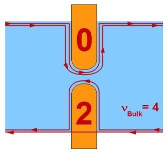
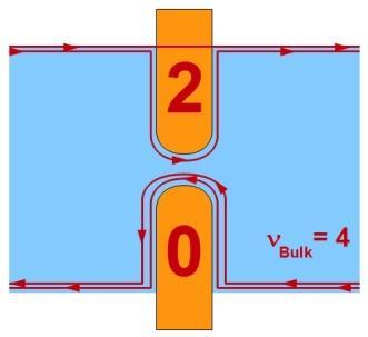
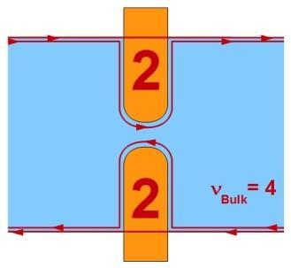
27 The oppurtunity of the Scanning Gate Microscopy Our technique allows to selectively control the channel trajectory Our idea: exploit the mobile depletion spot induced by the SGM to continuously tune d SGM tip n bulk = 4 two spin degenerate edges n=0 n=2 n=4


28 Experimental setup n=0 n=2 n=4 tip voltage=-10v edge-selector gate transmitted component 2DES mobility= 2.3x10 6 cm 2 /Vs e - density = 3.2x10 11 cm -2 depth= 55 nm tip reflected component source bias V=V AC + V DC SEM micrograph of the device Scheme of the electronic setup
![Calibration step Topography scan [nm]](/docs-images/87/97231295/images/29-5.jpg "80 0 Calibration SGM scan [e 2 /h] 4")
29 Calibration step Topography scan [nm] 80 0 Calibration SGM scan [e 2 /h] 4 0
![Calibration step differential conductance (e 2 /h) differential conductance (e 2 /h) Topography scan [nm] 80 0 Calibration SGM scan [e 2](/docs-images/87/97231295/images/30-7.jpg "/h] 4 3.0 2.5 0 the edges meet here 4.0 3.5 3.0 2.0 2.5 1.5 2.0 1.5 1.0 0.5 1.0 0 200 400 600 800 position (nm) 0.")
30 Calibration step differential conductance (e 2 /h) differential conductance (e 2 /h) Topography scan [nm] 80 0 Calibration SGM scan [e 2 /h] the edges meet here position (nm) position (mm)
![Imaging the inter-channel equilibration Calibration SGM scan [e 2 /h] 4 0 SGM](/docs-images/87/97231295/images/31-6.jpg "map of the I B signal: direct imaging of the equilibration process.")

31 Imaging the inter-channel equilibration Calibration SGM scan [e 2 /h] 4 0 SGM map of the I B signal: direct imaging of the equilibration process. Imaging the edge channel equilibration By grounding the upper contact an imbalance is established between the edges. grounded [e 2 /h] 1 0 Source bias: V AC =50mV, V DC =0mV
32 Imaging the inter-channel equilibration The profiles of G B (d) along the trajectory show a strict dependance on the local details Imaging the edge channel equilibration [e 2 /h] 1 0 Source bias: V AC =50mV, V DC =0mV

 along the")

33 Imaging the inter-channel equilibration SGM scan at zero magnetic field We can directly image the potential induced by the most important defects by means of a scan at zero magnetic field correlation found The profiles of G B (d) along the trajectory show a strict dependance on the local details Imaging the edge channel equilibration [e 2 /h] 1 0 Source bias: V AC =50mV, V DC =0mV


34 Tight binding simulations differential conductance G B (e 2 /h) Pictorial model for the disorder potential tip potential big impurities potential Simulations made by the theoretical group of Scuola Normale Superiore (Pisa, Italy) D. Venturelli, F. Taddei, V. Giovannetti and R.Fazio 0.40 background potential Experimental data Tight binding simulations scattering centers 0.20 [e 2 /h] 1 SGM map of the inter-channel equilibration in another device position (mm)
35 Next step: a simply connected MZI V in2 V in1 V in1 =0V Our idea to implement the Mach-Zehnder interferometer proposed by Giovannetti at al. V in2 =20mV I out2 I out1 Mixing (beam splitting) Mixing (beam splitting) d BS1 BS2 F If the electron mixing is coherent, it is possible to build an interferometer just by adding another selector gate F
36 Nonlinear regime The backscattered current is a function of the local imbalance DV(x) that depends on the specific scattering process.
37 Two mechanisms for the inter-channel scattering linear regime For low bias the only relevant mechanism is the elastic scattering induced by impurities, which determines an ohmic behavior (linear I-V) At high bias (Δμ ħω c ) vertical transition with photon emission are enabled (threshold and saturation)
38 Impact of the electron heating Electron heating due to injection of hot carriers: The relaxation of hot carriers induces a dramatic temperature increase. This is why the transition is smoothened and the threshold voltage reduced for high d
39 Conclusions We explored the use of the Scanning Gate Microscope to selectively control the edge channel trajectories Control of the edge channel trajectory allowed us to study their structure We built size-tunable QH circuits to directly image the equilibration between imbalanced co-propagating edges The comparison with the SGM scan at zero magnetic field revealed a correlation between the local potential and steps in the G B (d) curve Shift of the threshold voltage for the onset of photon emission is explained by a simple model for the electron heating new! Our last measurements on n=1 samples managed to image the fractional incompressible stripes within a single integer edge channel

40 Novel results: fractional structures in integer channels Beenakker* suggested that at the edge of a smooth integer edge a series of compressible/ incompressible fractional stripes can occur. We used the SGM technique to image them. *C. W. J. Beenakker, PRL 64, 216 (1990) Even though the electron temperature is quite high (400 mk), nonetheless the more robust fractions (1/3, 2/5) are visible. N. Paradiso et al., PRB (submitted).

41 Summary and outlook The SGM technique allows us to individually control the edge channel trajectory and study their structure first application With this extra degree of freedom we can build size-tunable QH circuits that allowed us to study the inter-channel mixing 600nm we estended this technique to detect fractional structures Coherent mixers can be exploited to implement a new class of quantum interferometers V 1 V 2 V in2 =20mV I 1 I 2 Mixing (beam splitting) Mixing (beam splitting) F Future directions: Interference of fractional quasi-particles?


 and www.vjnano.org. -N.")

 1038-1041. -J. Salfi, N.")


42 Thank you for your attention! Nicola Paradiso, Ph. D. student at the Scuola Normale Superiore, Pisa (Italy). References: -S. Roddaro, N. Paradiso, V. Pellegrini, G. Biasiol, L. Sorba, and F. Beltram: Tuning Nonlinear Charge Transport between Integer and Fractional Quantum Hall States ; Phys. Rev. Lett. 103, (2009) Selected for Viewpoints in Physics (APS) and -N. Paradiso, S. Heun, S. Roddaro, L. N. Pfeiffer, K. W. West, L. Sorba, G. Biasiol, and F. Beltram: Selective control of edgechannel trajectories by scanning gate microscopy, Physica E 42 (2010) J. Salfi, N. Paradiso, S. Roddaro, S. Heun, S. V. Nair, I. G. Savelyev, M. Blumin, F. Beltram, and H. E. Ruda: Probing the gatevoltage-dependent surface potential of individual InAs nanowires using random telegraph signals, ACS Nano 5 (2011) N. Paradiso, S. Heun, S. Roddaro, D. Venturelli, F. Taddei, V. Giovannetti, R. Fazio, G. Biasiol, L. Sorba, and F. Beltram: Spatially resolved analysis of edge-channel equilibration in quantum Hall circuits, Phys. Rev. B 83 (2011)
Nanomaterials Characterization by lowtemperature Scanning Probe Microscopy
 Nanomaterials Characterization by lowtemperature Scanning Probe Microscopy Stefan Heun NEST, Istituto Nanoscienze-CNR and Scuola Normale Superiore Piazza San Silvestro 12, 56127 Pisa, Italy e-mail: stefan.heun@nano.cnr.it
Scanning gate microscopy and individual control of edge-state transmission through a quantum point contact
 Scanning gate microscopy and individual control of edge-state transmission through a quantum point contact Stefan Heun NEST, CNR-INFM and Scuola Normale Superiore, Pisa, Italy Coworkers NEST, Pisa, Italy:
Observation of neutral modes in the fractional quantum hall effect regime. Aveek Bid
 Observation of neutral modes in the fractional quantum hall effect regime Aveek Bid Department of Physics, Indian Institute of Science, Bangalore Nature 585 466 (2010) Quantum Hall Effect Magnetic field
Charging and Kondo Effects in an Antidot in the Quantum Hall Regime
 Semiconductor Physics Group Cavendish Laboratory University of Cambridge Charging and Kondo Effects in an Antidot in the Quantum Hall Regime M. Kataoka C. J. B. Ford M. Y. Simmons D. A. Ritchie University
File name: Supplementary Information Description: Supplementary Figures and Supplementary References. File name: Peer Review File Description:
 File name: Supplementary Information Description: Supplementary Figures and Supplementary References File name: Peer Review File Description: Supplementary Figure Electron micrographs and ballistic transport
Electron Interferometer Formed with a Scanning Probe Tip and Quantum Point Contact Supplementary Information
 Electron Interferometer Formed with a Scanning Probe Tip and Quantum Point Contact Supplementary Information Section I: Experimental Details Here we elaborate on the experimental details described for
2D Materials Research Activities at the NEST lab in Pisa, Italy. Stefan Heun NEST, Istituto Nanoscienze-CNR and Scuola Normale Superiore, Pisa, Italy
 2D Materials Research Activities at the NEST lab in Pisa, Italy Stefan Heun NEST, Istituto Nanoscienze-CNR and Scuola Normale Superiore, Pisa, Italy 2D Materials Research Activities at the NEST lab in
Final Research Report: Electronic and spin properties of one-dimensional semiconductor systems
 Final Research Report: Electronic and spin properties of one-dimensional semiconductor systems Researcher: Sébastien Faniel Advisor: Sorin Melinte 1. Initial objectives The purpose of our project was to
Intrinsic Charge Fluctuations and Nuclear Spin Order in GaAs Nanostructures
 Physics Department, University of Basel Intrinsic Charge Fluctuations and Nuclear Spin Order in GaAs Nanostructures Dominik Zumbühl Department of Physics, University of Basel Basel QC2 Center and Swiss
Unconventional electron quantum optics in condensed matter systems
 Unconventional electron quantum optics in condensed matter systems Dario Ferraro Centre de Physique Théorique, Marseille nanoqt-2016, Kyiv, October 10, 2016 In collaboration with: J. Rech, T. Jonckheere,
Lecture 20 - Semiconductor Structures
 Lecture 0: Structures Kittel Ch 17, p 494-503, 507-511 + extra material in the class notes MOS Structure metal Layer Structure Physics 460 F 006 Lect 0 1 Outline What is a semiconductor Structure? Created
Physics of Semiconductors
 Physics of Semiconductors 13 th 2016.7.11 Shingo Katsumoto Department of Physics and Institute for Solid State Physics University of Tokyo Outline today Laughlin s justification Spintronics Two current
Electron counting with quantum dots
 Electron counting with quantum dots Klaus Ensslin Solid State Physics Zürich with S. Gustavsson I. Shorubalko R. Leturcq T. Ihn A. C. Gossard Time-resolved charge detection Single photon detection Time-resolved
Commensurability-dependent transport of a Wigner crystal in a nanoconstriction
 NPCQS2012, OIST Commensurability-dependent transport of a Wigner crystal in a nanoconstriction David Rees, RIKEN, Japan Kimitoshi Kono (RIKEN) Paul Leiderer (University of Konstanz) Hiroo Totsuji (Okayama
Measurements of quasi-particle tunneling in the υ = 5/2 fractional. quantum Hall state
 Measurements of quasi-particle tunneling in the υ = 5/2 fractional quantum Hall state X. Lin, 1, * C. Dillard, 2 M. A. Kastner, 2 L. N. Pfeiffer, 3 and K. W. West 3 1 International Center for Quantum Materials,
Semiconductor Nanowires. Stefan Heun NEST, Istituto Nanoscienze-CNR and Scuola Normale Superiore, Pisa, Italy
 Semiconductor Nanowires Stefan Heun NEST, Istituto Nanoscienze-CNR and Scuola Normale Superiore, Pisa, Italy Leaning Tower in Pisa Pisa and Hangzhou: Twin towns since 2008 Institute of Nanoscience- National
Quantum Transport in Nanostructured Graphene Antti-Pekka Jauho
 Quantum Transport in Nanostructured Graphene Antti-Pekka Jauho ICSNN, July 23 rd 2018, Madrid CNG Group Photo Three stories 1. Conductance quantization suppression in the Quantum Hall Regime, Caridad et
Lecture 20: Semiconductor Structures Kittel Ch 17, p , extra material in the class notes
 Lecture 20: Semiconductor Structures Kittel Ch 17, p 494-503, 507-511 + extra material in the class notes MOS Structure Layer Structure metal Oxide insulator Semiconductor Semiconductor Large-gap Semiconductor
Impact of disorder and topology in two dimensional systems at low carrier densities
 Impact of disorder and topology in two dimensional systems at low carrier densities A Thesis Submitted For the Degree of Doctor of Philosophy in the Faculty of Science by Mohammed Ali Aamir Department
Quantum Hall Effect in Graphene p-n Junctions
 Quantum Hall Effect in Graphene p-n Junctions Dima Abanin (MIT) Collaboration: Leonid Levitov, Patrick Lee, Harvard and Columbia groups UIUC January 14, 2008 Electron transport in graphene monolayer New
arxiv:cond-mat/ v1 [cond-mat.mes-hall] 18 Jul 2000
![arxiv:cond-mat/ v1 [cond-mat.mes-hall] 18 Jul 2000](/thumbs/87/96520166.jpg "arxiv:cond-mat/ v1 [cond-mat.mes-hall] 18 Jul 2000") Topographic Mapping of the Quantum Hall Liquid using a Few-Electron Bubble G. Finkelstein, P.I. Glicofridis, R.C. Ashoori Department of Physics and Center for Materials Science and Engineering, Massachusetts
Topographic Mapping of the Quantum Hall Liquid using a Few-Electron Bubble G. Finkelstein, P.I. Glicofridis, R.C. Ashoori Department of Physics and Center for Materials Science and Engineering, Massachusetts
Scanning Gate Microscopy (SGM) of semiconductor nanostructures
 of semiconductor nanostructures") Scanning Gate Microscopy (SGM) of semiconductor nanostructures H. Sellier, P. Liu, B. Sacépé, S. Huant Dépt NANO, Institut NEEL, Grenoble, France B. Hackens, F. Martins, V. Bayot UCL, Louvain-la-Neuve,
Scanning Gate Microscopy (SGM) of semiconductor nanostructures H. Sellier, P. Liu, B. Sacépé, S. Huant Dépt NANO, Institut NEEL, Grenoble, France B. Hackens, F. Martins, V. Bayot UCL, Louvain-la-Neuve,
Correlated 2D Electron Aspects of the Quantum Hall Effect
 Correlated 2D Electron Aspects of the Quantum Hall Effect Magnetic field spectrum of the correlated 2D electron system: Electron interactions lead to a range of manifestations 10? = 4? = 2 Resistance (arb.
From nanophysics research labs to cell phones. Dr. András Halbritter Department of Physics associate professor
 From nanophysics research labs to cell phones Dr. András Halbritter Department of Physics associate professor Curriculum Vitae Birth: 1976. High-school graduation: 1994. Master degree: 1999. PhD: 2003.
Quantum Confinement in Graphene
 Quantum Confinement in Graphene from quasi-localization to chaotic billards MMM dominikus kölbl 13.10.08 1 / 27 Outline some facts about graphene quasibound states in graphene numerical calculation of
Non-equilibrium Green s functions: Rough interfaces in THz quantum cascade lasers
 Non-equilibrium Green s functions: Rough interfaces in THz quantum cascade lasers Tillmann Kubis, Gerhard Klimeck Department of Electrical and Computer Engineering Purdue University, West Lafayette, Indiana
arxiv: v1 [cond-mat.mes-hall] 15 Mar 2010
![arxiv: v1 [cond-mat.mes-hall] 15 Mar 2010](/thumbs/92/109859238.jpg "arxiv: v1 [cond-mat.mes-hall] 15 Mar 2010") Quantum phases: years of the Aharonov-Bohm Effect and years of the Berry phase arxiv:.8v [cond-mat.mes-hall] Mar Inferring the transport properties of edge-states formed at quantum Hall based Aharonov-Bohm
Quantum phases: years of the Aharonov-Bohm Effect and years of the Berry phase arxiv:.8v [cond-mat.mes-hall] Mar Inferring the transport properties of edge-states formed at quantum Hall based Aharonov-Bohm
Hydrogenated Graphene
 Hydrogenated Graphene Stefan Heun NEST, Istituto Nanoscienze-CNR and Scuola Normale Superiore Pisa, Italy Outline Epitaxial Graphene Hydrogen Chemisorbed on Graphene Hydrogen-Intercalated Graphene Outline
(a) (b) Supplementary Figure 1. (a) (b) (a) Supplementary Figure 2. (a) (b) (c) (d) (e)
 (b) Supplementary Figure 1. (a) (b) (a) Supplementary Figure 2. (a) (b) (c) (d) (e)") (a) (b) Supplementary Figure 1. (a) An AFM image of the device after the formation of the contact electrodes and the top gate dielectric Al 2 O 3. (b) A line scan performed along the white dashed line
(a) (b) Supplementary Figure 1. (a) An AFM image of the device after the formation of the contact electrodes and the top gate dielectric Al 2 O 3. (b) A line scan performed along the white dashed line
Tunable All Electric Spin Polarizer. School of Electronics and Computing Systems University of Cincinnati, Cincinnati, Ohio 45221, USA
 Tunable All Electric Spin Polarizer J. Charles 1, N. Bhandari 1, J. Wan 1, M. Cahay 1,, and R. S. Newrock 1 School of Electronics and Computing Systems University of Cincinnati, Cincinnati, Ohio 451, USA
SUPPLEMENTARY FIGURES
 1 SUPPLEMENTARY FIGURES Supplementary Figure 1: Schematic representation of the experimental set up. The PC of the hot line being biased, the temperature raises. The temperature is extracted from noise
Out-of-equilibrium electron dynamics in photoexcited topological insulators studied by TR-ARPES
 Cliquez et modifiez le titre Out-of-equilibrium electron dynamics in photoexcited topological insulators studied by TR-ARPES Laboratoire de Physique des Solides Orsay, France June 15, 2016 Workshop Condensed
Quantum Optics with Propagating Microwaves in Superconducting Circuits. Io-Chun Hoi 許耀銓
 Quantum Optics with Propagating Microwaves in Superconducting Circuits 許耀銓 Outline Motivation: Quantum network Introduction to superconducting circuits Quantum nodes The single-photon router The cross-kerr
Chapter 3 Properties of Nanostructures
 Chapter 3 Properties of Nanostructures In Chapter 2, the reduction of the extent of a solid in one or more dimensions was shown to lead to a dramatic alteration of the overall behavior of the solids. Generally,
Screening Model of Magnetotransport Hysteresis Observed in arxiv:cond-mat/ v1 [cond-mat.mes-hall] 27 Jul Bilayer Quantum Hall Systems
![Screening Model of Magnetotransport Hysteresis Observed in arxiv:cond-mat/ v1 [cond-mat.mes-hall] 27 Jul Bilayer Quantum Hall Systems](/thumbs/76/74053861.jpg "Screening Model of Magnetotransport Hysteresis Observed in arxiv:cond-mat/ v1 [cond-mat.mes-hall] 27 Jul Bilayer Quantum Hall Systems") , Screening Model of Magnetotransport Hysteresis Observed in arxiv:cond-mat/0607724v1 [cond-mat.mes-hall] 27 Jul 2006 Bilayer Quantum Hall Systems Afif Siddiki, Stefan Kraus, and Rolf R. Gerhardts Max-Planck-Institut
, Screening Model of Magnetotransport Hysteresis Observed in arxiv:cond-mat/0607724v1 [cond-mat.mes-hall] 27 Jul 2006 Bilayer Quantum Hall Systems Afif Siddiki, Stefan Kraus, and Rolf R. Gerhardts Max-Planck-Institut
One-Dimensional Coulomb Drag: Probing the Luttinger Liquid State - I
 One-Dimensional Coulomb Drag: Probing the Luttinger Liquid State - Although the LL description of 1D interacting electron systems is now well established theoretically, experimental effort to study the
QS School Summary
 2018 NSF/DOE/AFOSR Quantum Science Summer School June 22, 2018 QS 3 2018 School Summary Kyle Shen (Cornell) Some Thank yous! A Big Thanks to Caroline Brockner!!! Also to our fantastic speakers! Kavli Institute
Quantum Transport in Disordered Topological Insulators
 Quantum Transport in Disordered Topological Insulators Vincent Sacksteder IV, Royal Holloway, University of London Quansheng Wu, ETH Zurich Liang Du, University of Texas Austin Tomi Ohtsuki and Koji Kobayashi,
 Original citation: Oswald, Josef and Roemer, Rudolf A.. (15) Imaging of condensed quantum states in the quantum hall effect regime. Physics Procedia, 75. pp. 314-325. 1.116/j.phpro.15.12.38 Permanent WRAP
Electrically Protected Valley-Orbit Qubit in Silicon
 Quantum Coherence Lab Zumbühl Group Electrically Protected Valley-Orbit Qubit in Silicon - FAM talk - Florian Froning 21.09.2018 1 Motivation I [1] Zehnder, L., Zeitschrift für Instrumentenkunde. 11: 275
Nuclear spin spectroscopy for semiconductor hetero and nano structures
 (Interaction and Nanostructural Effects in Low-Dimensional Systems) November 16th, Kyoto, Japan Nuclear spin spectroscopy for semiconductor hetero and nano structures Yoshiro Hirayama Tohoku University
Landau quantization, Localization, and Insulator-quantum. Hall Transition at Low Magnetic Fields
 Landau quantization, Localization, and Insulator-quantum Hall Transition at Low Magnetic Fields Tsai-Yu Huang a, C.-T. Liang a, Gil-Ho Kim b, C.F. Huang c, C.P. Huang a and D.A. Ritchie d a Department
QUANTUM INTERFERENCE IN SEMICONDUCTOR RINGS
 QUANTUM INTERFERENCE IN SEMICONDUCTOR RINGS PhD theses Orsolya Kálmán Supervisors: Dr. Mihály Benedict Dr. Péter Földi University of Szeged Faculty of Science and Informatics Doctoral School in Physics
SUPPLEMENTARY INFORMATION
 DOI: 1.138/NMAT3449 Topological crystalline insulator states in Pb 1 x Sn x Se Content S1 Crystal growth, structural and chemical characterization. S2 Angle-resolved photoemission measurements at various
Quantum Transport in One-Dimensional Systems
 Lecture 2 Quantum Transport in One-Dimensional Systems K J Thomas Department of Physics Central University of Kerala Kasaragod, Kerala Harish Chandra Research Institute, Allahabad February 23, 2016 ONE-DIMENSIONAL
Transport of Electrons on Liquid Helium across a Tunable Potential Barrier in a Point Contact-like Geometry
 Journal of Low Temperature Physics - QFS2009 manuscript No. (will be inserted by the editor) Transport of Electrons on Liquid Helium across a Tunable Potential Barrier in a Point Contact-like Geometry
Coulomb Drag in Graphene
 Graphene 2017 Coulomb Drag in Graphene -Toward Exciton Condensation Philip Kim Department of Physics, Harvard University Coulomb Drag Drag Resistance: R D = V 2 / I 1 Onsager Reciprocity V 2 (B)/ I 1 =
Quantum transport in nanoscale solids
 Quantum transport in nanoscale solids The Landauer approach Dietmar Weinmann Institut de Physique et Chimie des Matériaux de Strasbourg Strasbourg, ESC 2012 p. 1 Quantum effects in electron transport R.
Reviewers' comments: Reviewer #1 (Remarks to the Author):
:") Reviewers' comments: Reviewer #1 (Remarks to the Author): The authors present a paper, nicely showing and explaining different conductance plateus in InSb nanowire. I think these results are very important
Reviewers' comments: Reviewer #1 (Remarks to the Author): The authors present a paper, nicely showing and explaining different conductance plateus in InSb nanowire. I think these results are very important
Coherence and Correlations in Transport through Quantum Dots
 Coherence and Correlations in Transport through Quantum Dots Rolf J. Haug Abteilung Nanostrukturen Institut für Festkörperphysik and Laboratory for Nano and Quantum Engineering Gottfried Wilhelm Leibniz
Réunion erc. Gwendal Fève. Panel PE3 12 mn presentation 12 mn questions
 Réunion erc Gwendal Fève Panel PE3 12 mn presentation 12 mn questions Electron quantum optics in quantum Hall edge channels Gwendal Fève Laboratoire Pierre Aigrain, Ecole Normale Supérieure-CNRS Professor
Spin Lifetime Enhancement by Shear Strain in Thin Silicon-on-Insulator Films. Dmitry Osintsev, Viktor Sverdlov, and Siegfried Selberherr
 10.1149/05305.0203ecst The Electrochemical Society Spin Lifetime Enhancement by Shear Strain in Thin Silicon-on-Insulator Films Dmitry Osintsev, Viktor Sverdlov, and Siegfried Selberherr Institute for
Compositional mapping of semiconductor quantum dots by X-ray photoemission electron microscopy
 Compositional mapping of semiconductor quantum dots by X-ray photoemission electron microscopy Stefan Heun CNR-INFM, Italy, Laboratorio Nazionale TASC, Trieste and NEST-SNS, Pisa Outline A brief introduction
SPINTRONICS. Waltraud Buchenberg. Faculty of Physics Albert-Ludwigs-University Freiburg
 SPINTRONICS Waltraud Buchenberg Faculty of Physics Albert-Ludwigs-University Freiburg July 14, 2010 TABLE OF CONTENTS 1 WHAT IS SPINTRONICS? 2 MAGNETO-RESISTANCE STONER MODEL ANISOTROPIC MAGNETO-RESISTANCE
Electronic transport in low dimensional systems
 Electronic transport in low dimensional systems For example: 2D system l
Physics of Low-Dimensional Semiconductor Structures
 Physics of Low-Dimensional Semiconductor Structures Edited by Paul Butcher University of Warwick Coventry, England Norman H. March University of Oxford Oxford, England and Mario P. Tosi Scuola Normale
Coherent Electron Focussing in a Two-Dimensional Electron Gas.
 EUROPHYSICSLETTERS 15 April 1988 Europhys. Lett., 5 (8), pp. 721-725 (1988) Coherent Electron Focussing in a Two-Dimensional Electron Gas. H. VANHOUTEN(*),B. J. VANWEES(**), J. E. MOOIJ(**),C. W. J. BEENAKKER(*)
Vortices and superfluidity
 Vortices and superfluidity Vortices in Polariton quantum fluids We should observe a phase change by π and a density minimum at the core Michelson interferometry Forklike dislocation in interference pattern
Graphene Field effect transistors
 GDR Meso 2008 Aussois 8-11 December 2008 Graphene Field effect transistors Jérôme Cayssol CPMOH, UMR Université de Bordeaux-CNRS 1) Role of the contacts in graphene field effect transistors motivated by
Composite Dirac liquids
 Composite Dirac liquids Composite Fermi liquid non-interacting 3D TI surface Interactions Composite Dirac liquid ~ Jason Alicea, Caltech David Mross, Andrew Essin, & JA, Physical Review X 5, 011011 (2015)
Chapter 12. Nanometrology. Oxford University Press All rights reserved.
 Chapter 12 Nanometrology Introduction Nanometrology is the science of measurement at the nanoscale level. Figure illustrates where nanoscale stands in relation to a meter and sub divisions of meter. Nanometrology
SUPPLEMENTARY INFORMATION
 SUPPLEMENTARY INFORMATION DOI: 10.1038/NNANO.2011.138 Graphene Nanoribbons with Smooth Edges as Quantum Wires Xinran Wang, Yijian Ouyang, Liying Jiao, Hailiang Wang, Liming Xie, Justin Wu, Jing Guo, and
Part III: Impurities in Luttinger liquids
 Functional RG for interacting fermions... Part III: Impurities in Luttinger liquids 1. Luttinger liquids 2. Impurity effects 3. Microscopic model 4. Flow equations 5. Results S. Andergassen, T. Enss (Stuttgart)
Spectroscopies for Unoccupied States = Electrons
 Spectroscopies for Unoccupied States = Electrons Photoemission 1 Hole Inverse Photoemission 1 Electron Tunneling Spectroscopy 1 Electron/Hole Emission 1 Hole Absorption Will be discussed with core levels
Quantum Hall effect. Quantization of Hall resistance is incredibly precise: good to 1 part in I believe. WHY?? G xy = N e2 h.
 Quantum Hall effect V1 V2 R L I I x = N e2 h V y V x =0 G xy = N e2 h n.b. h/e 2 = 25 kohms Quantization of Hall resistance is incredibly precise: good to 1 part in 10 10 I believe. WHY?? Robustness Why
Observation of topological surface state quantum Hall effect in an intrinsic three-dimensional topological insulator
 Observation of topological surface state quantum Hall effect in an intrinsic three-dimensional topological insulator Authors: Yang Xu 1,2, Ireneusz Miotkowski 1, Chang Liu 3,4, Jifa Tian 1,2, Hyoungdo
Anisotropic spin splitting in InGaAs wire structures
 Available online at www.sciencedirect.com Physics Physics Procedia Procedia 3 (010) 00 (009) 155 159 000 000 14 th International Conference on Narrow Gap Semiconductors and Systems Anisotropic spin splitting
Surfaces, Interfaces, and Layered Devices
 Surfaces, Interfaces, and Layered Devices Building blocks for nanodevices! W. Pauli: God made solids, but surfaces were the work of Devil. Surfaces and Interfaces 1 Interface between a crystal and vacuum
Conductance quantization and quantum Hall effect
 UNIVERSITY OF LJUBLJANA FACULTY OF MATHEMATICS AND PHYSICS DEPARTMENT FOR PHYSICS Miha Nemevšek Conductance quantization and quantum Hall effect Seminar ADVISER: Professor Anton Ramšak Ljubljana, 2004
Single Photon Generation & Application
 Single Photon Generation & Application Photon Pair Generation: Parametric down conversion is a non-linear process, where a wave impinging on a nonlinear crystal creates two new light beams obeying energy
Application II: The Ballistic Field-E ect Transistor
 Chapter 1 Application II: The Ballistic Field-E ect Transistor 1.1 Introduction In this chapter, we apply the formalism we have developed for charge currents to understand the output characteristics of
Spin electronics at the nanoscale. Michel Viret Service de Physique de l Etat Condensé CEA Saclay France
 Spin electronics at the nanoscale Michel Viret Service de Physique de l Etat Condensé CEA Saclay France Principles of spin electronics: ferromagnetic metals spin accumulation Resistivity of homogeneous
Cooperative Phenomena
 Cooperative Phenomena Frankfurt am Main Kaiserslautern Mainz B1, B2, B4, B6, B13N A7, A9, A12 A10, B5, B8 Materials Design - Synthesis & Modelling A3, A8, B1, B2, B4, B6, B9, B11, B13N A5, A7, A9, A12,
What is Quantum Transport?
 What is Quantum Transport? Branislav K. Nikolić Department of Physics and Astronomy, University of Delaware, U.S.A. http://www.physics.udel.edu/~bnikolic Semiclassical Transport (is boring!) Bloch-Boltzmann
Lectures: Condensed Matter II 1 Electronic Transport in Quantum dots 2 Kondo effect: Intro/theory. 3 Kondo effect in nanostructures
 Lectures: Condensed Matter II 1 Electronic Transport in Quantum dots 2 Kondo effect: Intro/theory. 3 Kondo effect in nanostructures Luis Dias UT/ORNL Lectures: Condensed Matter II 1 Electronic Transport
Low-dimensional electron transport properties in InAs/AlGaSb mesoscopic structures
 Superlattices and Microstructures, Vol 21, No 1, 1997 Low-dimensional electron transport properties in InAs/AlGaSb mesoscopic structures M Inoue, T Sugihara, T Maemoto, S Sasa, H Dobashi, S Izumiya Department
Zooming in on the Quantum Hall Effect
 Zooming in on the Quantum Hall Effect Cristiane MORAIS SMITH Institute for Theoretical Physics, Utrecht University, The Netherlands Capri Spring School p.1/31 Experimental Motivation Historical Summary:
Advanced techniques Local probes, SNOM
 Advanced techniques Local probes, SNOM Principle Probe the near field electromagnetic field with a local probe near field probe propagating field evanescent Advanced techniques Local probes, SNOM Principle
Electron spins in nonmagnetic semiconductors
 Electron spins in nonmagnetic semiconductors Yuichiro K. Kato Institute of Engineering Innovation, The University of Tokyo Physics of non-interacting spins Optical spin injection and detection Spin manipulation
HYSWITCH Informal meeting Chersonissos - Crete September 15th 19th 2007,
 HYSWITCH Informal meeting Chersonissos - Crete September 15th 19th 27, Scuola Normale Superiore & NEST CNR-INFM I-56126 Pisa, Italy F. Carillo I. Batov G. Biasiol F. Deon F. Dolcini F. Giazotto V. Pellegrini
Quantum Hall Effect in Vanishing Magnetic Fields
 Quantum Hall Effect in Vanishing Magnetic Fields Wei Pan Sandia National Labs Sandia is a multi-mission laboratory operated by Sandia Corporation, a Lockheed Martin Company, for the United States Department
Electrical and Optical Properties. H.Hofmann
 Introduction to Nanomaterials Electrical and Optical Properties H.Hofmann Electrical Properties Ohm: G= σw/l where is the length of the conductor, measured in meters [m], A is the cross-section area of
SUPPLEMENTARY INFORMATION
 Valley-symmetry-preserved transport in ballistic graphene with gate-defined carrier guiding Minsoo Kim 1, Ji-Hae Choi 1, Sang-Hoon Lee 1, Kenji Watanabe 2, Takashi Taniguchi 2, Seung-Hoon Jhi 1, and Hu-Jong
Superconducting qubits (Phase qubit) Quantum informatics (FKA 172)
 Quantum informatics (FKA 172)") Superconducting qubits (Phase qubit) Quantum informatics (FKA 172) Thilo Bauch (bauch@chalmers.se) Quantum Device Physics Laboratory, MC2, Chalmers University of Technology Qubit proposals for implementing
Superconducting qubits (Phase qubit) Quantum informatics (FKA 172) Thilo Bauch (bauch@chalmers.se) Quantum Device Physics Laboratory, MC2, Chalmers University of Technology Qubit proposals for implementing
+ - Indirect excitons. Exciton: bound pair of an electron and a hole.
 Control of excitons in multi-layer van der Waals heterostructures E. V. Calman, C. J. Dorow, M. M. Fogler, L. V. Butov University of California at San Diego, S. Hu, A. Mishchenko, A. K. Geim University
Current mechanisms Exam January 27, 2012
 Current mechanisms Exam January 27, 2012 There are four mechanisms that typically cause currents to flow: thermionic emission, diffusion, drift, and tunneling. Explain briefly which kind of current mechanisms
Supplementary Methods A. Sample fabrication
 Supplementary Methods A. Sample fabrication Supplementary Figure 1(a) shows the SEM photograph of a typical sample, with three suspended graphene resonators in an array. The cross-section schematic is
Topological insulators
 http://www.physik.uni-regensburg.de/forschung/fabian Topological insulators Jaroslav Fabian Institute for Theoretical Physics University of Regensburg Stara Lesna, 21.8.212 DFG SFB 689 what are topological
Quantum Condensed Matter Physics Lecture 17
 Quantum Condensed Matter Physics Lecture 17 David Ritchie http://www.sp.phy.cam.ac.uk/drp/home 17.1 QCMP Course Contents 1. Classical models for electrons in solids. Sommerfeld theory 3. From atoms to
Classification of Solids
 Classification of Solids Classification by conductivity, which is related to the band structure: (Filled bands are shown dark; D(E) = Density of states) Class Electron Density Density of States D(E) Examples
Surface compositional gradients of InAs/GaAs quantum dots
 Surface compositional gradients of InAs/GaAs quantum dots S. Heun, G. Biasiol, V. Grillo, E. Carlino, and L. Sorba Laboratorio Nazionale TASC INFM-CNR, I-34012 Trieste, Italy G. B. Golinelli University
Supporting Online Material for
 www.sciencemag.org/cgi/content/full/326/5955/974/dc1 Supporting Online Material for Observation of Half-Quantum Vortices in an Exciton-Polariton Condensate K. G. Lagoudakis,* T. Ostatnický, A. V. Kavokin,
Majorana single-charge transistor. Reinhold Egger Institut für Theoretische Physik
 Majorana single-charge transistor Reinhold Egger Institut für Theoretische Physik Overview Coulomb charging effects on quantum transport through Majorana nanowires: Two-terminal device: Majorana singlecharge
Decay of spin polarized hot carrier current in a quasi. one-dimensional spin valve structure arxiv:cond-mat/ v1 [cond-mat.mes-hall] 10 Oct 2003
![Decay of spin polarized hot carrier current in a quasi. one-dimensional spin valve structure arxiv:cond-mat/ v1 [cond-mat.mes-hall] 10 Oct 2003](/thumbs/74/70335523.jpg "Decay of spin polarized hot carrier current in a quasi. one-dimensional spin valve structure arxiv:cond-mat/ v1 [cond-mat.mes-hall] 10 Oct 2003") Decay of spin polarized hot carrier current in a quasi one-dimensional spin valve structure arxiv:cond-mat/0310245v1 [cond-mat.mes-hall] 10 Oct 2003 S. Pramanik and S. Bandyopadhyay Department of Electrical
Decay of spin polarized hot carrier current in a quasi one-dimensional spin valve structure arxiv:cond-mat/0310245v1 [cond-mat.mes-hall] 10 Oct 2003 S. Pramanik and S. Bandyopadhyay Department of Electrical
Les états de bord d un. isolant de Hall atomique
 Les états de bord d un isolant de Hall atomique séminaire Atomes Froids 2/9/22 Nathan Goldman (ULB), Jérôme Beugnon and Fabrice Gerbier Outline Quantum Hall effect : bulk Landau levels and edge states
STM spectroscopy (STS)
") STM spectroscopy (STS) di dv 4 e ( E ev, r) ( E ) M S F T F Basic concepts of STS. With the feedback circuit open the variation of the tunneling current due to the application of a small oscillating voltage
STM spectroscopy (STS) di dv 4 e ( E ev, r) ( E ) M S F T F Basic concepts of STS. With the feedback circuit open the variation of the tunneling current due to the application of a small oscillating voltage
Quantum Wires and Quantum Point Contacts. Quantum conductance
 Quantum Wires and Quantum Point Contacts Quantum conductance Classification of quasi-1d systems 1. What is quantum of resistance in magnetic and transport measurements of nanostructures? Are these quanta
SUPPLEMENTARY INFORMATION
 doi:10.1038/nature12036 We provide in the following additional experimental data and details on our demonstration of an electrically pumped exciton-polariton laser by supplementing optical and electrical
How to use the simulator
 How to use the simulator Overview The application allows for the exploration of four quantum circuits in all. Each simulator grants the user a large amount of freedom in experments they wish to conduct.
Electric Field-Dependent Charge-Carrier Velocity in Semiconducting Carbon. Nanotubes. Yung-Fu Chen and M. S. Fuhrer
 Electric Field-Dependent Charge-Carrier Velocity in Semiconducting Carbon Nanotubes Yung-Fu Chen and M. S. Fuhrer Department of Physics and Center for Superconductivity Research, University of Maryland,