File name: Supplementary Information Description: Supplementary Figures and Supplementary References. File name: Peer Review File Description:
|
|
|
- Gervais Johnson
- 5 years ago
- Views:
Transcription
1 File name: Supplementary Information Description: Supplementary Figures and Supplementary References File name: Peer Review File Description:
2
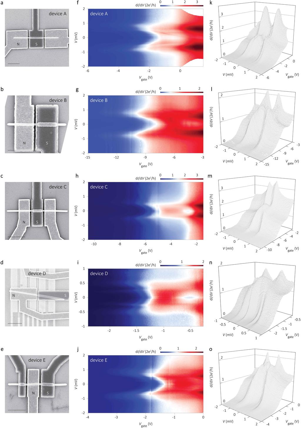
3 Supplementary Figure Electron micrographs and ballistic transport for all devices. a-e, Electron micrographs of all presented devices. N indicates the normal metal lead, S the superconducting lead. For three terminal devices, unlabelled leads are kept floated throughout the measurements. Scale bars for all images indicate µm. Data in Figure 3c (main text) is taken by sweeping the local gate underneath the uncovered wire section (see device D in panel d). f-j, Differential conductance of all devices in colour scale as a function of bias and gate voltage at zero magnetic field. k-o, Same as f-j but the differential conductance is on the vertical axis. All devices show quantized conductance, Andreev enhancement and an induced superconducting gap of.9 mv (A),.8 mv (B),.6 mv (C), and.5mv (D),.85 mv (E). Unintentional quantum dots are absent in all devices. Correspondence with the figures in main text: data in Figure and Figures 4b-d taken on device A, Figures a-d on device B, Figure e and Figure 3d on device C, Figure 3c on Device D, Figure 4a on device E.

4 Supplementary Figure Structure characterization and high-angle annular dark field analysis of the InSb-NbTi-NbTiN interface. a, High-resolution TEM cross-sectional image obtained by aligning the InSb nanowire along the zone axis in the [] orientation. Scale bar: nm. b, Fast Fourier transform (FFT) corresponding to a revealing the presence of both InSb and NbTiN. The NbTiN contribution leads to the formation of several Bragg spots on concentric rings, which provides evidence of the existence of several grains with different orientations in the original image. Each ring with different radius corresponds to a particular value of the interplanar spacing, i.e., it is the result of the reflections associated to a specific family of planes. Two different d-spacings have been identified and measured: d() =.49 nm and d() =.3 nm. They are indicated with yellow dashed lines in b. From these values, it is possible to determine the NbTiN 3
5 lattice parameter which we obtain to be.43 nm. On the other hand, the six {} reflections, indicated by a blue circle in the FFT, arise from the InSb region. From the calculated interplanar value of d {} =.3 nm we can estimate the InSb lattice parameter to be around.649 nm. The obtained lattice parameters for both NbTiN and InSb are in good agreement with the respective values reported in the literature. c, High-angle annular dark field (HAADF) scanning transmission electron microscopy (STEM) image of the device cross-section. Scale bar: 5 nm. d, Atomic resolution HAADF-STEM image of the interface for the region marked by the red square in c. Scale bar: nm. The highlighted area in green indicates the nm deep NbTi segregation into the InSb core. This effect is in good agreement with the EDX line scan, see Figure f (main text), which shows the NbTi region to be segregated nm deep into the InSb core on the {} facets. 4
6 a b c [] nanowire axis native surface Sulfur passivated surface E E E C E C E F E F metal InSb nanowire x [] metal E V metal E V x <> x <> d 8 G (e /h) 6 4 accumulation - 3 V gate (V) Sulfur passivation in-situ etch Supplementary Figure 3 Inclusion of Sulfur creates surface accumulation by band bending. a, A schematic of the device cross-section showing both the nanowire and the contact metal. Nanowire axis is along [] and the hexagonal facets have <> orientation. b, Band diagram for an InSb surface with <> orientation. Fermi level at the surface lies closer to the valence band. c, Band diagram for an InSb surface with <> orientation passivated with Sulfur-based solution. Inclusion of Sulfur at the surface counteracts the depletion and pins the Fermi level in the conduction band. This creates an electron-rich nanowire surface. d, Gate voltage response of nanowire devices with different contact preparation. A finite conductance for negative gate voltages indicates electron accumulation, highlighted in pink. Blue curve is taken from a device with contacts prepared using in-situ Ar plasma etch, red curve from a device with contacts prepared using Sulfur passivation. Both devices have identical geometries with a channel length of 5 nm. Devices with Sulfur passivated contact areas exhibit a negative threshold voltage (red arrow), in contrast to the devices with in-situ plasma etched contact areas (blue arrow). This typical characteristic measured on hundreds of nanowire devices indicates the doping effect of Sulfur inclusion at the InSb nanowire surface. Black arrows indicate the st, the 3rd, and the 5th quantized con- 5
7 ductance plateau. Upper plateaus appear at lower conductance values due to a finite contact resistance which is not subtracted from the conductance traces shown here. We also find that Sulfur passivated contacts show lower contact resistances than in-situ etched contacts, which can be seen from the difference in saturation conductance of both traces at high gate voltages. 6
8 a di/dv (e /h) c transmission G n G s st subband nd subband V gate (V) b d V gate (V) V gate (V) G n G s st subband nd subband V gate (V) Supplementary Figure 4 Subband mixing. a, b, The panels show the measured data taken from the main text, a from Figure e and b from Figure 3c. c, d, The panels show the transmission T of the first two subbands extracted from a and b, respectively, using G n = e /h T i and G s = 4e /h T i /( T i). When the transmission of the second subband becomes finite, the conductance modes mix, decreasing the Andreev enhancement. This effect shows up as a dip in G s when plotted as a function of gate voltage V gate. 7
9 a di/dv (e /h) μm f μm b di/dv (e /h).5 μm g.5 μm c di/dv (e /h).5 μm h.5 μm d di/dv (e /h) 5 μm i 5 μm e di/dv (e /h) μm j μm Supplementary Figure 5 Simulated conductance for varying mean free paths. a-e, The tunnelling conductance for different disorder strengths with mean free path l e ranging from µm to µm. f-j, The conductance in the plateau regime for different disorder strengths with mean free path l e ranging from µm to µm. For short l e, the Andreev enhancement is lower than that observed in our measurements and disorder-induced conductance fluctuations dominate the conductance for above-gap bias which we do not observe in our measurements. A good correspondence with the measurements is found for l e >.5 µm. We note that the details of the peak-dip structure in the Andreev conductance depend on several additional parameters of the system (e.g. barrier smoothness or disorder realization). In contrast, we find the conductance fluctuations above the gap to depend mainly on disorder strength, so that the combined analysis can be used as an estimate for the mean free path. The four symmetric peaks outside the gap around V ± mv indicate the induced superconducting gap for the higher two subbands (three subbands are occupied in total). Asymmetric conductance for different bias polarity is due to energy dependent transmission through the tunnel barrier, i.e., for positive bias V, effective QPC potential is lower. 8
.")

10 a.6 b.5 di/dv (e /h) di/dv (e /h) B (T).5 B (T).5 c d B = T.5 B = T di/dv (e /h). di/dv (e /h) B = T B = T Supplementary Figure 6 Magnetic field dependence of the induced gap and Andreev enhancement. a, Differential conductance di/dv of device B as a function of magnetic field B along the nanowire when the device is in the tunneling regime (gate voltage = V). We find an induced superconducting gap of.8 mv at zero magnetic field. Increasing magnetic fields increase the subgap conductance but a gap feature can be identified at least up to Tesla, indicating that the NbTiN leads are still superconducting. b, Differential conductance di/dv of the same device as a function of magnetic field B (along the wire axis) when the device is in the plateau regime (gate voltage = 6 V). At zero magnetic field, we find an enhancement of conductance up to a factor of.5 for subgap energies due to Andreev reflection. Increasing magnetic fields have a 9
11 negligible effect on the above-gap conductance. In contrast, the Andreev enhancement is suppressed at Tesla, a magnetic field at which the NbTiN leads are still superconducting. c, Line cuts from the data in a with vertical offsets.6 e /h. d, Line cuts from the data in b without offset. SUPPLEMENTARY REFERENCES Gobeli, G. W. & Allen, F. G. Photoelectric properties of cleaved GaAs, GaSb, InAs, and InSb surfaces; comparison with Si and Ge. Phys. Rev. 37, A45 (965) Kammhuber, J. et al. Conductance quantization at zero magnetic field in InSb nanowires. Nano Lett. 6, 348 (6)
Lecture 3: Heterostructures, Quasielectric Fields, and Quantum Structures
 Lecture 3: Heterostructures, Quasielectric Fields, and Quantum Structures MSE 6001, Semiconductor Materials Lectures Fall 2006 3 Semiconductor Heterostructures A semiconductor crystal made out of more
single-electron electron tunneling (SET)
") single-electron electron tunneling (SET) classical dots (SET islands): level spacing is NOT important; only the charging energy (=classical effect, many electrons on the island) quantum dots: : level spacing
single-electron electron tunneling (SET) classical dots (SET islands): level spacing is NOT important; only the charging energy (=classical effect, many electrons on the island) quantum dots: : level spacing
Title of file for HTML: Supplementary Information Description: Supplementary Figures and Supplementary References
 Title of file for HTML: Supplementary Information Description: Supplementary Figures and Supplementary References Supplementary Figure 1. SEM images of perovskite single-crystal patterned thin film with
SUPPLEMENTARY INFORMATION
 Collapse of superconductivity in a hybrid tin graphene Josephson junction array by Zheng Han et al. SUPPLEMENTARY INFORMATION 1. Determination of the electronic mobility of graphene. 1.a extraction from
SUPPLEMENTARY INFORMATION
 Electrical control of single hole spins in nanowire quantum dots V. S. Pribiag, S. Nadj-Perge, S. M. Frolov, J. W. G. van den Berg, I. van Weperen., S. R. Plissard, E. P. A. M. Bakkers and L. P. Kouwenhoven
Graphene photodetectors with ultra-broadband and high responsivity at room temperature
 SUPPLEMENTARY INFORMATION DOI: 10.1038/NNANO.2014.31 Graphene photodetectors with ultra-broadband and high responsivity at room temperature Chang-Hua Liu 1, You-Chia Chang 2, Ted Norris 1.2* and Zhaohui
SUPPLEMENTARY INFORMATION
 SUPPLEMENTARY INFORMATION DOI: 10.1038/NNANO.2011.138 Graphene Nanoribbons with Smooth Edges as Quantum Wires Xinran Wang, Yijian Ouyang, Liying Jiao, Hailiang Wang, Liming Xie, Justin Wu, Jing Guo, and
Supporting Online Material for
 www.sciencemag.org/cgi/content/full/320/5874/356/dc1 Supporting Online Material for Chaotic Dirac Billiard in Graphene Quantum Dots L. A. Ponomarenko, F. Schedin, M. I. Katsnelson, R. Yang, E. W. Hill,
SUPPLEMENTARY INFORMATION
 In the format provided by the authors and unedited. DOI:.38/NMAT4855 A magnetic heterostructure of topological insulators as a candidate for axion insulator M. Mogi, M. Kawamura, R. Yoshimi, A. Tsukazaki,
Electronic transport in low dimensional systems
 Electronic transport in low dimensional systems For example: 2D system l
Surfaces, Interfaces, and Layered Devices
 Surfaces, Interfaces, and Layered Devices Building blocks for nanodevices! W. Pauli: God made solids, but surfaces were the work of Devil. Surfaces and Interfaces 1 Interface between a crystal and vacuum
Indium arsenide quantum wire trigate metal oxide semiconductor field effect transistor
 JOURNAL OF APPLIED PHYSICS 99, 054503 2006 Indium arsenide quantum wire trigate metal oxide semiconductor field effect transistor M. J. Gilbert a and D. K. Ferry Department of Electrical Engineering and
Supplementary figures
 Supplementary figures Supplementary Figure 1. A, Schematic of a Au/SRO113/SRO214 junction. A 15-nm thick SRO113 layer was etched along with 30-nm thick SRO214 substrate layer. To isolate the top Au electrodes
Quantum Interference and Decoherence in Hexagonal Antidot Lattices
 Quantum Interference and Decoherence in Hexagonal Antidot Lattices Yasuhiro Iye, Masaaki Ueki, Akira Endo and Shingo Katsumoto Institute for Solid State Physics, University of Tokyo, -1- Kashiwanoha, Kashiwa,
Novel materials and nanostructures for advanced optoelectronics
 Novel materials and nanostructures for advanced optoelectronics Q. Zhuang, P. Carrington, M. Hayne, A Krier Physics Department, Lancaster University, UK u Brief introduction to Outline Lancaster University
Zeeman splitting of single semiconductor impurities in resonant tunneling heterostructures
 Superlattices and Microstructures, Vol. 2, No. 4, 1996 Zeeman splitting of single semiconductor impurities in resonant tunneling heterostructures M. R. Deshpande, J. W. Sleight, M. A. Reed, R. G. Wheeler
SUPPLEMENTARY INFORMATION
 Valley-symmetry-preserved transport in ballistic graphene with gate-defined carrier guiding Minsoo Kim 1, Ji-Hae Choi 1, Sang-Hoon Lee 1, Kenji Watanabe 2, Takashi Taniguchi 2, Seung-Hoon Jhi 1, and Hu-Jong
Observation of topological surface state quantum Hall effect in an intrinsic three-dimensional topological insulator
 Observation of topological surface state quantum Hall effect in an intrinsic three-dimensional topological insulator Authors: Yang Xu 1,2, Ireneusz Miotkowski 1, Chang Liu 3,4, Jifa Tian 1,2, Hyoungdo
SUPPLEMENTARY INFORMATION
 SUPPLEMENTARY INFORMATION SUPPLEMENTARY INFORMATION Trilayer graphene is a semimetal with a gate-tuneable band overlap M. F. Craciun, S. Russo, M. Yamamoto, J. B. Oostinga, A. F. Morpurgo and S. Tarucha
Enhancement-mode quantum transistors for single electron spin
 Purdue University Purdue e-pubs Other Nanotechnology Publications Birck Nanotechnology Center 8-1-2006 Enhancement-mode quantum transistors for single electron spin G. M. Jones B. H. Hu C. H. Yang M. J.
SUPPLEMENTARY FIGURES
 SUPPLEMENTARY FIGURES Sheet Resistance [k Ω ] 1.6 1.2.8.4 Sheet Resistance [k Ω ].32.3.28.26.24.22 Vg 1V Vg V (a).1.1.2.2.3 Temperature [K].2 (b) 2 4 6 8 1 12 14 16 18 µ H[Tesla].1 Hall Resistance [k Ω].1.2.3
Electrical and Optical Properties. H.Hofmann
 Introduction to Nanomaterials Electrical and Optical Properties H.Hofmann Electrical Properties Ohm: G= σw/l where is the length of the conductor, measured in meters [m], A is the cross-section area of
Reviewers' comments: Reviewer #1 (Remarks to the Author):
:") Reviewers' comments: Reviewer #1 (Remarks to the Author): The authors present a paper, nicely showing and explaining different conductance plateus in InSb nanowire. I think these results are very important
Reviewers' comments: Reviewer #1 (Remarks to the Author): The authors present a paper, nicely showing and explaining different conductance plateus in InSb nanowire. I think these results are very important
a b c Supplementary Figure S1
 a b c Supplementary Figure S1 AFM measurements of MoS 2 nanosheets prepared from the electrochemical Liintercalation and exfoliation. (a) AFM measurement of a typical MoS 2 nanosheet, deposited on Si/SiO
Quantum Hall circuits with variable geometry: study of the inter-channel equilibration by Scanning Gate Microscopy
 *nicola.paradiso@sns.it Nicola Paradiso Ph. D. Thesis Quantum Hall circuits with variable geometry: study of the inter-channel equilibration by Scanning Gate Microscopy N. Paradiso, Advisors: S. Heun,
Supplementary Information Interfacial Engineering of Semiconductor Superconductor Junctions for High Performance Micro-Coolers
 Supplementary Information Interfacial Engineering of Semiconductor Superconductor Junctions for High Performance Micro-Coolers D. Gunnarsson 1, J.S. Richardson-Bullock 2, M.J. Prest 2, H. Q. Nguyen 3,
2) Atom manipulation. Xe / Ni(110) Model: Experiment:
 Atom manipulation. Xe / Ni(110) Model: Experiment:") 2) Atom manipulation D. Eigler & E. Schweizer, Nature 344, 524 (1990) Xe / Ni(110) Model: Experiment: G.Meyer, et al. Applied Physics A 68, 125 (1999) First the tip is approached close to the adsorbate
2) Atom manipulation D. Eigler & E. Schweizer, Nature 344, 524 (1990) Xe / Ni(110) Model: Experiment: G.Meyer, et al. Applied Physics A 68, 125 (1999) First the tip is approached close to the adsorbate
Formation of unintentional dots in small Si nanostructures
 Superlattices and Microstructures, Vol. 28, No. 5/6, 2000 doi:10.1006/spmi.2000.0942 Available online at http://www.idealibrary.com on Formation of unintentional dots in small Si nanostructures L. P. ROKHINSON,
Temperature dependence of Andreev spectra in a superconducting carbon nanotube quantum dot
 Temperature dependence of Andreev spectra in a superconducting carbon nanotube quantum dot A. Kumar, M. Gaim, D. Steininger, A. Levy Yeyati, A. Martín-Rodero, A. K. Hüttel, and C. Strunk Phys. Rev. B 89,
(a) (b) Supplementary Figure 1. (a) (b) (a) Supplementary Figure 2. (a) (b) (c) (d) (e)
 (b) Supplementary Figure 1. (a) (b) (a) Supplementary Figure 2. (a) (b) (c) (d) (e)") (a) (b) Supplementary Figure 1. (a) An AFM image of the device after the formation of the contact electrodes and the top gate dielectric Al 2 O 3. (b) A line scan performed along the white dashed line
(a) (b) Supplementary Figure 1. (a) An AFM image of the device after the formation of the contact electrodes and the top gate dielectric Al 2 O 3. (b) A line scan performed along the white dashed line
SUPPLEMENTARY INFORMATION
 In the format provided by the authors and unedited. DOI: 10.1038/NPHYS4186 Stripes Developed at the Strong Limit of Nematicity in FeSe film Wei Li 1,2,3*, Yan Zhang 2,3,4,5, Peng Deng 1, Zhilin Xu 1, S.-K.
MSE 310/ECE 340: Electrical Properties of Materials Fall 2014 Department of Materials Science and Engineering Boise State University
 MSE 310/ECE 340: Electrical Properties of Materials Fall 2014 Department of Materials Science and Engineering Boise State University Practice Final Exam 1 Read the questions carefully Label all figures
Classification of Solids
 Classification of Solids Classification by conductivity, which is related to the band structure: (Filled bands are shown dark; D(E) = Density of states) Class Electron Density Density of States D(E) Examples
STM spectroscopy (STS)
") STM spectroscopy (STS) di dv 4 e ( E ev, r) ( E ) M S F T F Basic concepts of STS. With the feedback circuit open the variation of the tunneling current due to the application of a small oscillating voltage
STM spectroscopy (STS) di dv 4 e ( E ev, r) ( E ) M S F T F Basic concepts of STS. With the feedback circuit open the variation of the tunneling current due to the application of a small oscillating voltage
Supplementary Materials for
 www.sciencemag.org/content/349/6253/1202/suppl/dc1 Supplementary Materials for Critical behavior at a dynamic vortex insulator-to-metal transition Nicola Poccia, Tatyana I. Baturina, Francesco Coneri,
Supplementary Figure 1: Micromechanical cleavage of graphene on oxygen plasma treated Si/SiO2. Supplementary Figure 2: Comparison of hbn yield.
 1 2 3 4 Supplementary Figure 1: Micromechanical cleavage of graphene on oxygen plasma treated Si/SiO 2. Optical microscopy images of three examples of large single layer graphene flakes cleaved on a single
Impact of disorder and topology in two dimensional systems at low carrier densities
 Impact of disorder and topology in two dimensional systems at low carrier densities A Thesis Submitted For the Degree of Doctor of Philosophy in the Faculty of Science by Mohammed Ali Aamir Department
Surface Defects on Natural MoS 2
 Supporting Information: Surface Defects on Natural MoS 2 Rafik Addou 1*, Luigi Colombo 2, and Robert M. Wallace 1* 1 Department of Materials Science and Engineering, The University of Texas at Dallas,
SUPPLEMENTARY INFORMATION
 Supplementary Information: Photocurrent generation in semiconducting and metallic carbon nanotubes Maria Barkelid 1*, Val Zwiller 1 1 Kavli Institute of Nanoscience, Delft University of Technology, Delft,
FIG. 1: (Supplementary Figure 1: Large-field Hall data) (a) AHE (blue) and longitudinal
 (a) AHE (blue) and longitudinal") FIG. 1: (Supplementary Figure 1: Large-field Hall data) (a) AHE (blue) and longitudinal MR (red) of device A at T =2 K and V G - V G 0 = 100 V. Bold blue line is linear fit to large field Hall data (larger
FIG. 1: (Supplementary Figure 1: Large-field Hall data) (a) AHE (blue) and longitudinal MR (red) of device A at T =2 K and V G - V G 0 = 100 V. Bold blue line is linear fit to large field Hall data (larger
Anisotropic spin splitting in InGaAs wire structures
 Available online at www.sciencedirect.com Physics Physics Procedia Procedia 3 (010) 00 (009) 155 159 000 000 14 th International Conference on Narrow Gap Semiconductors and Systems Anisotropic spin splitting
Tunable All Electric Spin Polarizer. School of Electronics and Computing Systems University of Cincinnati, Cincinnati, Ohio 45221, USA
 Tunable All Electric Spin Polarizer J. Charles 1, N. Bhandari 1, J. Wan 1, M. Cahay 1,, and R. S. Newrock 1 School of Electronics and Computing Systems University of Cincinnati, Cincinnati, Ohio 451, USA
Avalanche breakdown. Impact ionization causes an avalanche of current. Occurs at low doping
 Avalanche breakdown Impact ionization causes an avalanche of current Occurs at low doping Zener tunneling Electrons tunnel from valence band to conduction band Occurs at high doping Tunneling wave decays
8. Schottky contacts / JFETs
 Technische Universität Graz Institute of Solid State Physics 8. Schottky contacts / JFETs Nov. 21, 2018 Technische Universität Graz Institute of Solid State Physics metal - semiconductor contacts Photoelectric
SUPPLEMENTARY INFORMATION
 SUPPLEMENTARY INFORMATION DOI: 10.1038/NNANO.2014.16 Electrical detection of charge current-induced spin polarization due to spin-momentum locking in Bi 2 Se 3 by C.H. Li, O.M.J. van t Erve, J.T. Robinson,
Cross-Section Scanning Tunneling Microscopy of InAs/GaSb Superlattices
 Cross-Section Scanning Tunneling Microscopy of InAs/GaSb Superlattices Cecile Saguy A. Raanan, E. Alagem and R. Brener Solid State Institute. Technion, Israel Institute of Technology, Haifa 32000.Israel
What is Quantum Transport?
 What is Quantum Transport? Branislav K. Nikolić Department of Physics and Astronomy, University of Delaware, U.S.A. http://www.physics.udel.edu/~bnikolic Semiclassical Transport (is boring!) Bloch-Boltzmann
Graphene and Carbon Nanotubes
 Graphene and Carbon Nanotubes 1 atom thick films of graphite atomic chicken wire Novoselov et al - Science 306, 666 (004) 100μm Geim s group at Manchester Novoselov et al - Nature 438, 197 (005) Kim-Stormer
Quantum physics in quantum dots
 Quantum physics in quantum dots Klaus Ensslin Solid State Physics Zürich AFM nanolithography Multi-terminal tunneling Rings and dots Time-resolved charge detection Moore s Law Transistors per chip 10 9
Tunneling Spectroscopy of PCCO
 Tunneling Spectroscopy of PCCO Neesha Anderson and Amlan Biswas Department of Physics, University of Florida, Gainesville, Florida Abstract A point-contact probe capable of operating down to temperatures
SUPPLEMENTARY INFORMATION
 Dirac electron states formed at the heterointerface between a topological insulator and a conventional semiconductor 1. Surface morphology of InP substrate and the device Figure S1(a) shows a 10-μm-square
Supplementary Information
 Supplementary Information I. Sample details In the set of experiments described in the main body, we study an InAs/GaAs QDM in which the QDs are separated by 3 nm of GaAs, 3 nm of Al 0.3 Ga 0.7 As, and
Current mechanisms Exam January 27, 2012
 Current mechanisms Exam January 27, 2012 There are four mechanisms that typically cause currents to flow: thermionic emission, diffusion, drift, and tunneling. Explain briefly which kind of current mechanisms
How a single defect can affect silicon nano-devices. Ted Thorbeck
 How a single defect can affect silicon nano-devices Ted Thorbeck tedt@nist.gov The Big Idea As MOS-FETs continue to shrink, single atomic scale defects are beginning to affect device performance Gate Source
SUPPLEMENTARY INFORMATION
 Dirac cones reshaped by interaction effects in suspended graphene D. C. Elias et al #1. Experimental devices Graphene monolayers were obtained by micromechanical cleavage of graphite on top of an oxidized
Majorana single-charge transistor. Reinhold Egger Institut für Theoretische Physik
 Majorana single-charge transistor Reinhold Egger Institut für Theoretische Physik Overview Coulomb charging effects on quantum transport through Majorana nanowires: Two-terminal device: Majorana singlecharge
Transport through Andreev Bound States in a Superconductor-Quantum Dot-Graphene System
 Transport through Andreev Bound States in a Superconductor-Quantum Dot-Graphene System Nadya Mason Travis Dirk, Yung-Fu Chen, Cesar Chialvo Taylor Hughes, Siddhartha Lal, Bruno Uchoa Paul Goldbart University
Schottky diodes. JFETs - MESFETs - MODFETs
 Technische Universität Graz Institute of Solid State Physics Schottky diodes JFETs - MESFETs - MODFETs Quasi Fermi level When the charge carriers are not in equilibrium the Fermi energy can be different
Superconductivity at nanoscale
 Superconductivity at nanoscale Superconductivity is the result of the formation of a quantum condensate of paired electrons (Cooper pairs). In small particles, the allowed energy levels are quantized and
SUPPLEMENTARY INFORMATION
 DOI: 10.1038/NPHYS576 Colossal Enhancement of Spin-Orbit Coupling in Weakly Hydrogenated Graphene Jayakumar Balakrishnan 1,, *, Gavin Kok Wai Koon 1,, 3, *, Manu Jaiswal 1,,, Antonio H. Castro Neto 1,,
Universal valence-band picture of. the ferromagnetic semiconductor GaMnAs
 Universal valence-band picture of the ferromagnetic semiconductor GaMnAs Shinobu Ohya *, Kenta Takata, and Masaaki Tanaka Department of Electrical Engineering and Information Systems, The University of
Charging and Kondo Effects in an Antidot in the Quantum Hall Regime
 Semiconductor Physics Group Cavendish Laboratory University of Cambridge Charging and Kondo Effects in an Antidot in the Quantum Hall Regime M. Kataoka C. J. B. Ford M. Y. Simmons D. A. Ritchie University
Supporting information
 Supporting information Design, Modeling and Fabrication of CVD Grown MoS 2 Circuits with E-Mode FETs for Large-Area Electronics Lili Yu 1*, Dina El-Damak 1*, Ujwal Radhakrishna 1, Xi Ling 1, Ahmad Zubair
A New Method of Scanning Tunneling Spectroscopy for Study of the Energy Structure of Semiconductors and Free Electron Gas in Metals
 SCANNING Vol. 19, 59 5 (1997) Received April 1, 1997 FAMS, Inc. Accepted May, 1997 A New Method of Scanning Tunneling Spectroscopy for Study of the Energy Structure of Semiconductors and Free Electron
The quantum Hall effect under the influence of a top-gate and integrating AC lock-in measurements
 The quantum Hall effect under the influence of a top-gate and integrating AC lock-in measurements TOBIAS KRAMER 1,2, ERIC J. HELLER 2,3, AND ROBERT E. PARROTT 4 arxiv:95.3286v1 [cond-mat.mes-hall] 2 May
Supplementary Figure 1 Experimental setup for crystal growth. Schematic drawing of the experimental setup for C 8 -BTBT crystal growth.
 Supplementary Figure 1 Experimental setup for crystal growth. Schematic drawing of the experimental setup for C 8 -BTBT crystal growth. Supplementary Figure 2 AFM study of the C 8 -BTBT crystal growth
Edge conduction in monolayer WTe 2
 In the format provided by the authors and unedited. DOI: 1.138/NPHYS491 Edge conduction in monolayer WTe 2 Contents SI-1. Characterizations of monolayer WTe2 devices SI-2. Magnetoresistance and temperature
1 Corresponding author:
 Scanning Tunneling Microscopy Study of Cr-doped GaN Surface Grown by RF Plasma Molecular Beam Epitaxy Muhammad B. Haider, Rong Yang, Hamad Al-Brithen, Costel Constantin, Arthur R. Smith 1, Gabriel Caruntu
Application II: The Ballistic Field-E ect Transistor
 Chapter 1 Application II: The Ballistic Field-E ect Transistor 1.1 Introduction In this chapter, we apply the formalism we have developed for charge currents to understand the output characteristics of
Supplementary Information
 Supplementary Information Supplementary Figures Supplementary figure S1: Characterisation of the electron beam intensity profile. (a) A 3D plot of beam intensity (grey value) with position, (b) the beam
Quantized Electrical Conductance of Carbon nanotubes(cnts)
") Quantized Electrical Conductance of Carbon nanotubes(cnts) By Boxiao Chen PH 464: Applied Optics Instructor: Andres L arosa Abstract One of the main factors that impacts the efficiency of solar cells is
Quantized Electrical Conductance of Carbon nanotubes(cnts) By Boxiao Chen PH 464: Applied Optics Instructor: Andres L arosa Abstract One of the main factors that impacts the efficiency of solar cells is
Charge spectrometry with a strongly coupled superconducting single-electron transistor
 PHYSICAL REVIEW B, VOLUME 64, 245116 Charge spectrometry with a strongly coupled superconducting single-electron transistor C. P. Heij, P. Hadley, and J. E. Mooij Applied Physics and Delft Institute of
Performance Analysis of Ultra-Scaled InAs HEMTs
 Purdue University Purdue e-pubs Birck and NCN Publications Birck Nanotechnology Center 2009 Performance Analysis of Ultra-Scaled InAs HEMTs Neerav Kharche Birck Nanotechnology Center and Purdue University,
Scanning gate microscopy and individual control of edge-state transmission through a quantum point contact
 Scanning gate microscopy and individual control of edge-state transmission through a quantum point contact Stefan Heun NEST, CNR-INFM and Scuola Normale Superiore, Pisa, Italy Coworkers NEST, Pisa, Italy:
Supporting Information. Nanoscale control of rewriteable doping patterns in pristine graphene/boron nitride heterostructures
 Supporting Information Nanoscale control of rewriteable doping patterns in pristine graphene/boron nitride heterostructures Jairo Velasco Jr. 1,5,, Long Ju 1,, Dillon Wong 1,, Salman Kahn 1, Juwon Lee
SUPPLEMENTARY INFORMATION
 DOI: 10.1038/NCHEM.2491 Experimental Realization of Two-dimensional Boron Sheets Baojie Feng 1, Jin Zhang 1, Qing Zhong 1, Wenbin Li 1, Shuai Li 1, Hui Li 1, Peng Cheng 1, Sheng Meng 1,2, Lan Chen 1 and
Supplementary Figure S1. AFM images of GraNRs grown with standard growth process. Each of these pictures show GraNRs prepared independently,
 Supplementary Figure S1. AFM images of GraNRs grown with standard growth process. Each of these pictures show GraNRs prepared independently, suggesting that the results is reproducible. Supplementary Figure
Solid Surfaces, Interfaces and Thin Films
 Hans Lüth Solid Surfaces, Interfaces and Thin Films Fifth Edition With 427 Figures.2e Springer Contents 1 Surface and Interface Physics: Its Definition and Importance... 1 Panel I: Ultrahigh Vacuum (UHV)
High Power Diode Lasers
 Lecture 10/1 High Power Diode Lasers Low Power Lasers (below tenth of mw) - Laser as a telecom transmitter; - Laser as a spectroscopic sensor; - Laser as a medical diagnostic tool; - Laser as a write-read
Barrier Photodetectors for High Sensitivity and High Operating Temperature Infrared Sensors
 Barrier Photodetectors for High Sensitivity and High Operating Temperature Infrared Sensors Philip Klipstein General Review of Barrier Detectors 1) Higher operating temperature, T OP 2) Higher signal to
Chapter 3 Properties of Nanostructures
 Chapter 3 Properties of Nanostructures In Chapter 2, the reduction of the extent of a solid in one or more dimensions was shown to lead to a dramatic alteration of the overall behavior of the solids. Generally,
NONLINEAR TRANSPORT IN BALLISTIC SEMICONDUCTOR DIODES WITH NEGATIVE EFFECTIVE MASS CARRIERS
 NONLINEAR TRANSPORT IN BALLISTIC SEMICONDUCTOR DIODES WITH NEGATIVE EFFECTIVE MASS CARRIERS B. R. Perkins, Jun Liu, and A. Zaslavsky, Div. of Engineering Brown University Providence, RI 02912, U.S.A.,
Commensurability-dependent transport of a Wigner crystal in a nanoconstriction
 NPCQS2012, OIST Commensurability-dependent transport of a Wigner crystal in a nanoconstriction David Rees, RIKEN, Japan Kimitoshi Kono (RIKEN) Paul Leiderer (University of Konstanz) Hiroo Totsuji (Okayama
Supplementary Figure 1. Supplementary Figure 1 Characterization of another locally gated PN junction based on boron
 Supplementary Figure 1 Supplementary Figure 1 Characterization of another locally gated PN junction based on boron nitride and few-layer black phosphorus (device S1). (a) Optical micrograph of device S1.
Broken Symmetry States and Divergent Resistance in Suspended Bilayer Graphene
 Broken Symmetry States and Divergent Resistance in Suspended Bilayer Graphene The Harvard community has made this article openly available. Please share how this access benefits you. Your story matters.
Quantum behavior of graphene transistors near the scaling limit
 Supplementary Information for Quantum behavior of graphene transistors near the scaling limit Yanqing Wu *, Vasili Perebeinos, Yu-ming Lin, Tony Low, Fengnian Xia and Phaedon Avouris * IBM Thomas J. Watson
Lecture 9: Metal-semiconductor junctions
 Lecture 9: Metal-semiconductor junctions Contents 1 Introduction 1 2 Metal-metal junction 1 2.1 Thermocouples.......................... 2 3 Schottky junctions 4 3.1 Forward bias............................
Low-dimensional electron transport properties in InAs/AlGaSb mesoscopic structures
 Superlattices and Microstructures, Vol 21, No 1, 1997 Low-dimensional electron transport properties in InAs/AlGaSb mesoscopic structures M Inoue, T Sugihara, T Maemoto, S Sasa, H Dobashi, S Izumiya Department
Principles and Applications of Superconducting Quantum Interference Devices (SQUIDs)
") Principles and Applications of Superconducting Quantum Interference Devices (SQUIDs) PHY 300 - Junior Phyics Laboratory Syed Ali Raza Roll no: 2012-10-0124 LUMS School of Science and Engineering Thursday,
Principles and Applications of Superconducting Quantum Interference Devices (SQUIDs) PHY 300 - Junior Phyics Laboratory Syed Ali Raza Roll no: 2012-10-0124 LUMS School of Science and Engineering Thursday,
NiCl2 Solution concentration. Etching Duration. Aspect ratio. Experiment Atmosphere Temperature. Length(µm) Width (nm) Ar:H2=9:1, 150Pa
 Width (nm) Ar:H2=9:1, 150Pa") Experiment Atmosphere Temperature #1 # 2 # 3 # 4 # 5 # 6 # 7 # 8 # 9 # 10 Ar:H2=9:1, 150Pa Ar:H2=9:1, 150Pa Ar:H2=9:1, 150Pa Ar:H2=9:1, 150Pa Ar:H2=9:1, 150Pa Ar:H2=9:1, 150Pa Ar:H2=9:1, 150Pa Ar:H2=9:1,
Experiment Atmosphere Temperature #1 # 2 # 3 # 4 # 5 # 6 # 7 # 8 # 9 # 10 Ar:H2=9:1, 150Pa Ar:H2=9:1, 150Pa Ar:H2=9:1, 150Pa Ar:H2=9:1, 150Pa Ar:H2=9:1, 150Pa Ar:H2=9:1, 150Pa Ar:H2=9:1, 150Pa Ar:H2=9:1,
Quantum Effects in Thermal and Thermo-Electric Transport in Semiconductor Nanost ructu res
 Physica Scripta. Vol. T49, 441-445, 1993 Quantum Effects in Thermal and Thermo-Electric Transport in Semiconductor Nanost ructu res L. W. Molenkamp, H. van Houten and A. A. M. Staring Philips Research
ELEC 4700 Assignment #2
 ELEC 4700 Assignment #2 Question 1 (Kasop 4.2) Molecular Orbitals and Atomic Orbitals Consider a linear chain of four identical atoms representing a hypothetical molecule. Suppose that each atomic wavefunction
SUPPLEMENTARY INFORMATION
 SUPPLEMENTARY INFORMATION Insulating Interlocked Ferroelectric and Structural Antiphase Domain Walls in Multiferroic YMnO 3 T. Choi 1, Y. Horibe 1, H. T. Yi 1,2, Y. J. Choi 1, Weida. Wu 1, and S.-W. Cheong
Nanoelectronics 09. Atsufumi Hirohata Department of Electronics. Quick Review over the Last Lecture
 Nanoelectronics 09 Atsufumi Hirohata Department of Electronics 13:00 Monday, 12/February/2018 (P/T 006) Quick Review over the Last Lecture ( Field effect transistor (FET) ): ( Drain ) current increases
Saroj P. Dash. Chalmers University of Technology. Göteborg, Sweden. Microtechnology and Nanoscience-MC2
 Silicon Spintronics Saroj P. Dash Chalmers University of Technology Microtechnology and Nanoscience-MC2 Göteborg, Sweden Acknowledgement Nth Netherlands University of Technology Sweden Mr. A. Dankert Dr.
Electrical Contacts to Carbon Nanotubes Down to 1nm in Diameter
 1 Electrical Contacts to Carbon Nanotubes Down to 1nm in Diameter Woong Kim, Ali Javey, Ryan Tu, Jien Cao, Qian Wang, and Hongjie Dai* Department of Chemistry and Laboratory for Advanced Materials, Stanford
Supporting Information for Quantized Conductance and Large g-factor Anisotropy in InSb Quantum Point Contacts
 Supporting Information for Quantized Conductance and Large g-factor Anisotropy in InSb Quantum Point Contacts Fanming Qu, Jasper van Veen, Folkert K. de Vries, Arjan J. A. Beukman, Michael Wimmer, Wei
Electron Interferometer Formed with a Scanning Probe Tip and Quantum Point Contact Supplementary Information
 Electron Interferometer Formed with a Scanning Probe Tip and Quantum Point Contact Supplementary Information Section I: Experimental Details Here we elaborate on the experimental details described for
Introduction to Nanotechnology Chapter 5 Carbon Nanostructures Lecture 1
 Introduction to Nanotechnology Chapter 5 Carbon Nanostructures Lecture 1 ChiiDong Chen Institute of Physics, Academia Sinica chiidong@phys.sinica.edu.tw 02 27896766 Carbon contains 6 electrons: (1s) 2,
EXPLORING SCANNING PROBE MICROSCOPY WITH MATHEMATICA
 EXPLORING SCANNING PROBE MICROSCOPY WITH MATHEMATICA Dror Sarid University of Arizona A WILEY-1NTERSCIENCE PUBLICATION JOHN WILEY & SONS, INC. New York Chichester Weinheim Brisbane Singapore Toronto CONTENTS