Intrinsic Charge Fluctuations and Nuclear Spin Order in GaAs Nanostructures
|
|
|
- Abigail Hart
- 6 years ago
- Views:
Transcription
1 Physics Department, University of Basel Intrinsic Charge Fluctuations and Nuclear Spin Order in GaAs Nanostructures Dominik Zumbühl Department of Physics, University of Basel Basel QC2 Center and Swiss Nanoscience Institute SNI Scuola Enrico Fermi, Varenna, Quantum Spintronics and Related Phenomena fundamental, intrinsic double-dot physics nuclear spin order in a Luttinger liquid?

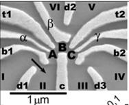
2 500 nm 50 nm

3 Device: Double Dot with Charge Sensors surface-gate defined on a GaAs 2D electron gas (2DEG) charge sensors: quantum dots wafer material from Zimmermann, Gossard, UCSB device layout: Barthel, Marcus et al. PRL 2009, PRB2010
 Fermi wavelength F ~ 50 nm mean")
4 GaAs 2D Electron Gas (2DEG) A. Johnson density n = 2 x cm -2 mobility ~ cm 2 /(Vs) Fermi wavelength F ~ 50 nm mean free path ~ micron J. Zimmerman and A. C. Gossard, UC Santa Barbara

5 Lateral Depletion Gating, Ohmic Contacts depletion region A. Johnson quantum point contact voltage adjustable depletion area B. van Wees et al., PRL 1988 D. Wharam et al., J. Phys. C

6 Forming a Quantum Dot
7 Coulomb Blockade, Charging Energy capacitance of dot C small size of dot ~ 10 nm charging energy ~ mev Coulomb blockade peaks: resonant transport through dot 0.15 g (e 2 /h) N = classical, not quantum V (mv)


8 Quantum Confinement Energy harmonic potential complicated potential average level spacing ev to mev quantum mechanics


9 Coulomb Diamonds kt ~ ev ~ mev Ec ~ mev 200nm V SD I differential conductance: peaks when current through dot is changing


10 Sequential Tunneling, Excited-State Spectroscopy lab to investigate quantum levels in device!! A B C quantum confinement energies internal excitations (spin) A B C 2ES 1ES 2ES GS 1ES -ev SD GS -ev SD 2ES 1ES GS -ev SD only one excess electron can be on dot (charging energy)

11 Charge sensing of Single Electrons QPC g QPC sensor sensitivity quantum point contact g / g QPC ~ 5 % QPC conductance add one electron to dot N empty dot g dot N+1 time one-electron dot


12 T E ~ 50 mk dot charge sensor: sensitivity dg/g ~100% Barthel, Marcus et al. PRL 2009, PRB2010 M. Field et al., PRL Elzermann et al., PRB, Nature 2003/2004
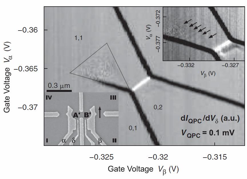
 (1,2) (2,2) (0,1)")
 can empty both dots")

13 Charge Stability Diagram (0,2) (1,2) (2,2) (0,1) (1,1) (2,1) (2,0) (0,0) (1,0) can empty both dots add electrons one by one Elzermann et al., PRB, Nature 2003/2004
14 (0,0) (1,1) Transition lock-in measurement ( 1, 1 ) ( 0, 1 ) ( 1, 0 ) ( 0, 0 ) Van der Wiel et al., RMP2003
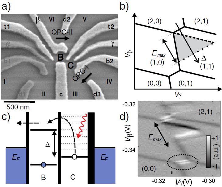
15 Time scale of charge fluctuations: an example assumptions: dot levels E ~100 ev below reservoirs electron T = 150 mk (13 ev) ~ 10 MHz (100 ns, 0.5 mk) charge fluctuation rate ~ here: ~ 200 s (average time for electron to leave dot) but: exponentially sensitive to temperature, level positions e.g. for T = 100 mk, 10 ms fluctuations destroy spin qubit information appear in T1 measurement but easy to remedy: lower tunneling rates / temperatures / level energies
16 Double Dot Charge Fluctuations and Metastable States present for all vertices, not only for (0,0)-(1,1) if excited-state not metastable fluctuations present, but not directly visible (interdot tunneling faster than detector) charge fluctuations present throughout charge stability diagram rate strongly energy dependent fluctuations destroy spin qubit information but easy to remedy: lower tunneling rates / temperatures / level energies

17 external energy absorption

18 extrinsic effect, energy absorption
19 Summary intrinsic charge fluctuations and metastable states in GaAs few-electron double dots - charge fluctuations due to sequential tunneling exchange with reservoirs - intrinsic effect, no energy absorption, not sensor back-action - fluctuations easily visible for metastable states - experiment and model in quantitative agreement - control fluctuation rate a) exponentially with level energy, temperature b) linear in bare reservoir tunnel rate work in progress to be submitted
 in Luttinger liquids (1D) GaAs wire carbon nanotube Braunecker, Simon & Loss, PRB2009,")
20 Nuclear Helimagnets induced by hyperfine coupling and strongly interacting electron system (ee interaction) in Luttinger liquids (1D) GaAs wire carbon nanotube Braunecker, Simon & Loss, PRB2009, PRL 2008
21 Spin-Selective Peierls Transition in a Luttinger Liquid Peierls: metal insulator transition induced by F /2 periodic potential spin selective Peierls transition Braunecker, Japardize, Klinovaja & Loss, PRB 2010 induced by - spin-orbit coupling - nuclear Helimagnet (equivalent) freeze ½ of modes spin selective, g = 1 e 2 /h
22 GaAs Cleaved Edge Overgrowth Quantum Wires ultraclean, ballistic, micron long wires, density-tunable with gate probably the best established realization of a Luttinger liquid in nature Pfeiffer et al., JCG 1993 Yacoby et al., SSC 1996 Yacoby et al., PRL 1996 Picciotto et al., PRL 2000 Picciotto et al., Nature 2001 Auslaender et al., Science 2002 Tserkovnyak et al., PRL 2002 Tserkovnyak et al., PRB 2003 Auslaender et al., Science 2005 Steinberg et al., PRB 2006 Steinberg et al., NP 2008 Barak et al., NP 2010
 overgrow cleavage plane with modulation doping sequence gives charges at edge few modes strong overlap 2DEG to edge intimate 2D-1D coupling c) use gate to deplete 2DEG below control edge")
23 GaAs Cleaved Edge Overgrowth (CEO) Quantum Wires a) AlGaAs/GaAs quantum well Si doping above well 2D electron gas (2DEG) 500 nm deep n ~ cm -2, > 10 6 cm 2 /(Vs) tungsten surface gate cleave in UHV b) overgrow cleavage plane with modulation doping sequence gives charges at edge few modes strong overlap 2DEG to edge intimate 2D-1D coupling c) use gate to deplete 2DEG below control edge density & # modes Pfeiffer et al., JCG 1993 Yacoby et al., SSC 1996 Yacoby et al., PRL 1996
 rectangular (QW)/ triangular (heterointerface) modes")
 very large subband spacing (many mev, from B-field data) Yacoby et")
24 Gate-Voltage: Conductance Plateaus varying side-gate V S 300 mk y mean free path >10 m (flat plateaus) rectangular (QW)/ triangular (heterointerface) modes conductance quantization not universal (not 2e 2 /h multiples) but repeatable (QW width dependent) very large subband spacing (many mev, from B-field data) Yacoby et al., SSC 1996
25 Low-Temperature T < 300 mk Wire Transport Basel measurements on Yacoby / Pfeiffer wires weak, short, not-flat plateaus, low density
26 Two Parallel Wires: upper wire (UW), lower wire (LW) more recently grown, higher quality samples V G y z x UW LW long, flat plateaus (2 m wire) V G tunes simultaneously UW and LW density additional complication: both wires conduct in parallel most simple model: g = g UW + g LW
27 Identify Modes / Wires y z x LW mode 1 + UW mode 1

28 Identify Modes: B-dependence y z x
29 Identify Modes / Wires y z x LW mode 1 + UW mode 1 + LW + UW mode 2 mode 2 (weak coupling)
30 Electron Temperature Measurements use two independent methods 1. on-chip FQHE thermometer: upper bound on T: T < 30 mk 2. independent cool down with Coulomb blockade thermometers (Meschke & Pekola, Aalto Univ., Finland) T = 11 mk for identical setup, cold finger, chip carrier etc. both of these independent measurements give temperatures much smaller than 80 mk

31 Cool Metallic CBT thermometer to 7.5 ± 0.2 mk M. Meschke, J. Pekola Aalto University


32 Nuclear Ordering Temperature: Theory Estimates Braunecker, Simon & Loss, PRB 2009
33 Non-Universal Conductance Quantization A. Yacoby, L. Pfeiffer et al., PRL 1996 T = 0.3K NMR & magnon experiments in progress, C. Scheller
34 Reduced Conductance Quantization Model 1: non-interacting electrons non-interacting electron in both contacts and wires Landauer Formula, no disorder: multiples of 2e 2 /h reduced g: transmission T < 1 (disorder) ruled out by a) energy independence T (flat, long plateaus) b) temperature dependence for energy independent T
35 Reduced Conductance Quantization Model 2: interacting electrons, Luttinger liquid theory infinite Luttinger liquid: g = N K 2e 2 /h (Luttinger interaction parameter K 1) Apel & Rice, PRB 1982 Kane & Fisher, PRL, PRB 1992 clean, finite wire with Fermi liquid (non-interacting) leads g = N 2e 2 /h Maslov & Stone, PRB 1995 with weak disorder: reduced g with power-law due to wire ee only (contact resistance outside wire, unaffected by wire interactions plus weak scattering inside wire with LL features) finite conductance ~ 1/L at T = 0 Ogata & Fukuyama PRL 1994 Tarucha et al., SSC 1994 Maslov, PRB 1995 ruled out by long, flat plateaus (K would depend on plateau position)
36 Reduced Conductance Quantization Model 3: Boltzmann 2D-1D contact scattering model coupling a) from 2D to few (~ 4-8) mode, semi-infinite wire, with weak LL correl. b) from semi-infinite wire to single mode wire BS : wire back scattering LL enhanced at low-t 2D : 2D-1D scattering LL suppressed at low-t (vanishing LL DOS) G arising from contacts, not single mode wire 2D-1D coupling requires momentum scattering rule out, since this predicts G -> 0 at T -> 0 (not seen) Yacoby et al., PRL 1996 Picciotto et al., PRL 2000
37 Reduced Conductance Quantization Model 4: Wigner Crystal, Heisenberg Chain at very low densities, large r S finite length Wigner Crystal antiferromagnetic Heisenberg chain, exponentially small exchange coupling J Matveev PRL, PRB 2004 present wires not in this very low density regime also, this model predicts qualitatively opposite T-dependence: low T<<J: 2e 2 /h high T>>J: 1e 2 /h
38 Summary & Outlook charge fluctuations in GaAs few-electron double dots - thermally activated, two-step sequential tunneling process - intrinsic effect, no energy absorption, not sensor back-action - causes qubit decoherence: improve with low tunneling, low T evidence for nuclear-spin order in GaAs quantum wires -wire g ~ 1e 2 /h for T < 80 mk (g ~ 2 e 2 /2 at high T) - sample electrons cool to ~ 10 mk (CBT) - not inconsistent with spin-selective Peierls transition in a Luttinger liquid and a nuclear helimagnet both experiments: work in progress


39 Acknowledgements charge fluctuations GaAs double dots Daniel Biesinger, Basel Christian Scheller, Basel theory B. Braunecker, UA Madrid GaAs 2DEG wafers J. Zimmermann, A. C. Gossard, UC Santa Barbara nuclear spins quantum wires experiments C. Scheller, Basel samples, discussions G. Barak, A. Yacoby Harvard University theory B. Braunecker, UA Madrid D. Loss, Basel P. Simon, U Paris Sud CEO wires growth L. Pfeiffer, K. West Bell Labs & Princeton CBT thermometers M. Meschke, J. Pekola Aalto University, Helsinki Daniel Biesinger Christian Scheller
Lecture 2: Double quantum dots
 Lecture 2: Double quantum dots Basics Pauli blockade Spin initialization and readout in double dots Spin relaxation in double quantum dots Quick Review Quantum dot Single spin qubit 1 Qubit states: 450
Electrical Control of Single Spins in Semiconductor Quantum Dots Jason Petta Physics Department, Princeton University
 Electrical Control of Single Spins in Semiconductor Quantum Dots Jason Petta Physics Department, Princeton University g Q 2 m T + S Mirror U 3 U 1 U 2 U 3 Mirror Detector See Hanson et al., Rev. Mod. Phys.
Nanoscience, MCC026 2nd quarter, fall Quantum Transport, Lecture 1/2. Tomas Löfwander Applied Quantum Physics Lab
 Nanoscience, MCC026 2nd quarter, fall 2012 Quantum Transport, Lecture 1/2 Tomas Löfwander Applied Quantum Physics Lab Quantum Transport Nanoscience: Quantum transport: control and making of useful things
Lectures: Condensed Matter II 1 Electronic Transport in Quantum dots 2 Kondo effect: Intro/theory. 3 Kondo effect in nanostructures
 Lectures: Condensed Matter II 1 Electronic Transport in Quantum dots 2 Kondo effect: Intro/theory. 3 Kondo effect in nanostructures Luis Dias UT/ORNL Lectures: Condensed Matter II 1 Electronic Transport
Quantum Information Processing with Semiconductor Quantum Dots
 Quantum Information Processing with Semiconductor Quantum Dots slides courtesy of Lieven Vandersypen, TU Delft Can we access the quantum world at the level of single-particles? in a solid state environment?
Correlated 2D Electron Aspects of the Quantum Hall Effect
 Correlated 2D Electron Aspects of the Quantum Hall Effect Magnetic field spectrum of the correlated 2D electron system: Electron interactions lead to a range of manifestations 10? = 4? = 2 Resistance (arb.
Lecture 8, April 12, 2017
 Lecture 8, April 12, 2017 This week (part 2): Semiconductor quantum dots for QIP Introduction to QDs Single spins for qubits Initialization Read-Out Single qubit gates Book on basics: Thomas Ihn, Semiconductor
Quantum Information Processing with Semiconductor Quantum Dots. slides courtesy of Lieven Vandersypen, TU Delft
 Quantum Information Processing with Semiconductor Quantum Dots slides courtesy of Lieven Vandersypen, TU Delft Can we access the quantum world at the level of single-particles? in a solid state environment?
Electron counting with quantum dots
 Electron counting with quantum dots Klaus Ensslin Solid State Physics Zürich with S. Gustavsson I. Shorubalko R. Leturcq T. Ihn A. C. Gossard Time-resolved charge detection Single photon detection Time-resolved
Chapter 3 Properties of Nanostructures
 Chapter 3 Properties of Nanostructures In Chapter 2, the reduction of the extent of a solid in one or more dimensions was shown to lead to a dramatic alteration of the overall behavior of the solids. Generally,
Controlling Spin Qubits in Quantum Dots. C. M. Marcus Harvard University
 Controlling Spin Qubits in Quantum Dots C. M. Marcus Harvard University 1 Controlling Spin Qubits in Quantum Dots C. M. Marcus Harvard University GaAs Experiments: David Reilly (Univ. Sydney) Edward Laird
Electronic transport in low dimensional systems
 Electronic transport in low dimensional systems For example: 2D system l
Commensurability-dependent transport of a Wigner crystal in a nanoconstriction
 NPCQS2012, OIST Commensurability-dependent transport of a Wigner crystal in a nanoconstriction David Rees, RIKEN, Japan Kimitoshi Kono (RIKEN) Paul Leiderer (University of Konstanz) Hiroo Totsuji (Okayama
Charges and Spins in Quantum Dots
 Charges and Spins in Quantum Dots L.I. Glazman Yale University Chernogolovka 2007 Outline Confined (0D) Fermi liquid: Electron-electron interaction and ground state properties of a quantum dot Confined
Kondo effect in multi-level and multi-valley quantum dots. Mikio Eto Faculty of Science and Technology, Keio University, Japan
 Kondo effect in multi-level and multi-valley quantum dots Mikio Eto Faculty of Science and Technology, Keio University, Japan Outline 1. Introduction: next three slides for quantum dots 2. Kondo effect
Quantum physics in quantum dots
 Quantum physics in quantum dots Klaus Ensslin Solid State Physics Zürich AFM nanolithography Multi-terminal tunneling Rings and dots Time-resolved charge detection Moore s Law Transistors per chip 10 9
Tunable Non-local Spin Control in a Coupled Quantum Dot System. N. J. Craig, J. M. Taylor, E. A. Lester, C. M. Marcus
 Tunable Non-local Spin Control in a Coupled Quantum Dot System N. J. Craig, J. M. Taylor, E. A. Lester, C. M. Marcus Department of Physics, Harvard University, Cambridge, Massachusetts 02138, USA M. P.
Transport through Andreev Bound States in a Superconductor-Quantum Dot-Graphene System
 Transport through Andreev Bound States in a Superconductor-Quantum Dot-Graphene System Nadya Mason Travis Dirk, Yung-Fu Chen, Cesar Chialvo Taylor Hughes, Siddhartha Lal, Bruno Uchoa Paul Goldbart University
single-electron electron tunneling (SET)
") single-electron electron tunneling (SET) classical dots (SET islands): level spacing is NOT important; only the charging energy (=classical effect, many electrons on the island) quantum dots: : level spacing
single-electron electron tunneling (SET) classical dots (SET islands): level spacing is NOT important; only the charging energy (=classical effect, many electrons on the island) quantum dots: : level spacing
LECTURE 2: Thermometry
 LECTURE 2: Thermometry Tunnel barrier Examples of aluminium-oxide tunnel barriers Basics of tunnel junctions E 1 2 Tunneling from occupied states to empty states V Metal Insulator Metal (NIN) tunnel junction
Developing Quantum Logic Gates: Spin-Resonance-Transistors
 Developing Quantum Logic Gates: Spin-Resonance-Transistors H. W. Jiang (UCLA) SRT: a Field Effect Transistor in which the channel resistance monitors electron spin resonance, and the resonance frequency
Carbon Nanotubes part 2 CNT s s as a toy model for basic science. Niels Bohr Institute School 2005
 Carbon Nanotubes part 2 CNT s s as a toy model for basic science Niels Bohr Institute School 2005 1 Carbon Nanotubes as a model system 2 Christian Schönenberger University of Basel B. Babic W. Belzig M.
Laurens W. Molenkamp. Physikalisches Institut, EP3 Universität Würzburg
 Laurens W. Molenkamp Physikalisches Institut, EP3 Universität Würzburg Onsager Coefficients I electric current density J particle current density J Q heat flux, heat current density µ chemical potential
CIRCUIT QUANTUM ELECTRODYNAMICS WITH ELECTRONS ON HELIUM
 CIRCUIT QUANTUM ELECTRODYNAMICS WITH ELECTRONS ON HELIUM David Schuster Assistant Professor University of Chicago Chicago Ge Yang Bing Li Michael Geracie Yale Andreas Fragner Rob Schoelkopf Useful cryogenics
Single Spin Qubits, Qubit Gates and Qubit Transfer with Quantum Dots
 International School of Physics "Enrico Fermi : Quantum Spintronics and Related Phenomena June 22-23, 2012 Varenna, Italy Single Spin Qubits, Qubit Gates and Qubit Transfer with Quantum Dots Seigo Tarucha
Scanning gate microscopy and individual control of edge-state transmission through a quantum point contact
 Scanning gate microscopy and individual control of edge-state transmission through a quantum point contact Stefan Heun NEST, CNR-INFM and Scuola Normale Superiore, Pisa, Italy Coworkers NEST, Pisa, Italy:
Three-terminal quantum-dot thermoelectrics
 Three-terminal quantum-dot thermoelectrics Björn Sothmann Université de Genève Collaborators: R. Sánchez, A. N. Jordan, M. Büttiker 5.11.2013 Outline Introduction Quantum dots and Coulomb blockade Quantum
Quantum Hall circuits with variable geometry: study of the inter-channel equilibration by Scanning Gate Microscopy
 *nicola.paradiso@sns.it Nicola Paradiso Ph. D. Thesis Quantum Hall circuits with variable geometry: study of the inter-channel equilibration by Scanning Gate Microscopy N. Paradiso, Advisors: S. Heun,
Quantum Effects in Thermal and Thermo-Electric Transport in Semiconductor Nanost ructu res
 Physica Scripta. Vol. T49, 441-445, 1993 Quantum Effects in Thermal and Thermo-Electric Transport in Semiconductor Nanost ructu res L. W. Molenkamp, H. van Houten and A. A. M. Staring Philips Research
Imaging a Single-Electron Quantum Dot
 Imaging a Single-Electron Quantum Dot Parisa Fallahi, 1 Ania C. Bleszynski, 1 Robert M. Westervelt, 1* Jian Huang, 1 Jamie D. Walls, 1 Eric J. Heller, 1 Micah Hanson, 2 Arthur C. Gossard 2 1 Division of
Surfaces, Interfaces, and Layered Devices
 Surfaces, Interfaces, and Layered Devices Building blocks for nanodevices! W. Pauli: God made solids, but surfaces were the work of Devil. Surfaces and Interfaces 1 Interface between a crystal and vacuum
Kondo Physics in Nanostructures. A.Abdelrahman Department of Physics University of Basel Date: 27th Nov. 2006/Monday meeting
 Kondo Physics in Nanostructures A.Abdelrahman Department of Physics University of Basel Date: 27th Nov. 2006/Monday meeting Kondo Physics in Nanostructures Kondo Effects in Metals: magnetic impurities
Nuclear spin spectroscopy for semiconductor hetero and nano structures
 (Interaction and Nanostructural Effects in Low-Dimensional Systems) November 16th, Kyoto, Japan Nuclear spin spectroscopy for semiconductor hetero and nano structures Yoshiro Hirayama Tohoku University
Single Electron Transistor (SET)
") Single Electron Transistor (SET) SET: e - e - dot A single electron transistor is similar to a normal transistor (below), except 1) the channel is replaced by a small dot. C g 2) the dot is separated from
Single Electron Transistor (SET) SET: e - e - dot A single electron transistor is similar to a normal transistor (below), except 1) the channel is replaced by a small dot. C g 2) the dot is separated from
An RF Circuit Model for Carbon Nanotubes
 IEEE TRANSACTIONS ON NANOTECHNOLOGY, VOL. 2, NO. 1, MARCH 2003 55 An RF Circuit Model for Carbon Nanotubes Abstract We develop an RF circuit model for single walled carbon nanotubes for both dc and capacitively
Electronic refrigeration and thermometry in nanostructures at low temperatures
 Electronic refrigeration and thermometry in nanostructures at low temperatures Jukka Pekola Low Temperature Laboratory Aalto University, Finland Nanostructures Temperature Energy relaxation Thermometry
Quantum information processing in semiconductors
 FIRST 2012.8.14 Quantum information processing in semiconductors Yasuhiro Tokura (University of Tsukuba, NTT BRL) Part I August 14, afternoon I Part II August 15, morning I Part III August 15, morning
arxiv:cond-mat/ v1 5 Dec 2003
 Signatures of spin-charge separation in double quantum-wire tunneling Yaroslav Tserkovnyak and Bertrand I. Halperin Lyman Laboratory of Physics, Harvard University, Cambridge, Massachusetts 02138, USA
Conductance of a quantum wire at low electron density
 Conductance of a quantum wire at low electron density Konstantin Matveev Materials Science Division Argonne National Laboratory Argonne National Laboratory Boulder School, 7/25/2005 1. Quantum wires and
Physics and Material Science of Semiconductor Nanostructures
 Physics and Material Science of Semiconductor Nanostructures PHYS 570P Prof. Oana Malis Email: omalis@purdue.edu Course website: http://www.physics.purdue.edu/academic_programs/courses/phys570p/ 1 Introduction
No reason one cannot have double-well structures: With MBE growth, can control well thicknesses and spacings at atomic scale.
 The story so far: Can use semiconductor structures to confine free carriers electrons and holes. Can get away with writing Schroedinger-like equation for Bloch envelope function to understand, e.g., -confinement
Single Electron Tunneling Examples
 Single Electron Tunneling Examples Danny Porath 2002 (Schönenberger et. al.) It has long been an axiom of mine that the little things are infinitely the most important Sir Arthur Conan Doyle Books and
The Physics of Nanoelectronics
 The Physics of Nanoelectronics Transport and Fluctuation Phenomena at Low Temperatures Tero T. Heikkilä Low Temperature Laboratory, Aalto University, Finland OXFORD UNIVERSITY PRESS Contents List of symbols
Nano-Electro-Mechanical Systems (NEMS) in the Quantum Limit
 in the Quantum Limit") Nano-Electro-Mechanical Systems (NEMS) in the Quantum Limit Eva Weig, now postdoc at University of California at Santa Barbara. Robert H. Blick, University of Wisconsin-Madison, Electrical & Computer Engineering,
Nano-Electro-Mechanical Systems (NEMS) in the Quantum Limit Eva Weig, now postdoc at University of California at Santa Barbara. Robert H. Blick, University of Wisconsin-Madison, Electrical & Computer Engineering,
Electronic Quantum Transport in Mesoscopic Semiconductor Structures
 Thomas Ihn Electronic Quantum Transport in Mesoscopic Semiconductor Structures With 90 Illustrations, S in Full Color Springer Contents Part I Introduction to Electron Transport l Electrical conductance
File name: Supplementary Information Description: Supplementary Figures and Supplementary References. File name: Peer Review File Description:
 File name: Supplementary Information Description: Supplementary Figures and Supplementary References File name: Peer Review File Description: Supplementary Figure Electron micrographs and ballistic transport
The effect of surface conductance on lateral gated quantum devices in Si/SiGe heterostructures
 The effect of surface conductance on lateral gated quantum devices in Si/SiGe heterostructures The MIT Faculty has made this article openly available. Please share how this access benefits you. Your story
Spontaneous Spin Polarization in Quantum Wires
 Spontaneous Spin Polarization in Quantum Wires Julia S. Meyer The Ohio State University with A.D. Klironomos K.A. Matveev 1 Why ask this question at all GaAs/AlGaAs heterostucture 2D electron gas Quantum
InAs/GaSb A New 2D Topological Insulator
 InAs/GaSb A New 2D Topological Insulator 1. Old Material for New Physics 2. Quantized Edge Modes 3. Adreev Reflection 4. Summary Rui-Rui Du Rice University Superconductor Hybrids Villard de Lans, France
Quantum transport in nanoscale solids
 Quantum transport in nanoscale solids The Landauer approach Dietmar Weinmann Institut de Physique et Chimie des Matériaux de Strasbourg Strasbourg, ESC 2012 p. 1 Quantum effects in electron transport R.
Dipole-coupling a single-electron double quantum dot to a microwave resonator
 Dipole-coupling a single-electron double quantum dot to a microwave resonator 200 µm J. Basset, D.-D. Jarausch, A. Stockklauser, T. Frey, C. Reichl, W. Wegscheider, T. Ihn, K. Ensslin and A. Wallraff Quantum
Measurements of quasi-particle tunneling in the υ = 5/2 fractional. quantum Hall state
 Measurements of quasi-particle tunneling in the υ = 5/2 fractional quantum Hall state X. Lin, 1, * C. Dillard, 2 M. A. Kastner, 2 L. N. Pfeiffer, 3 and K. W. West 3 1 International Center for Quantum Materials,
Formation of unintentional dots in small Si nanostructures
 Superlattices and Microstructures, Vol. 28, No. 5/6, 2000 doi:10.1006/spmi.2000.0942 Available online at http://www.idealibrary.com on Formation of unintentional dots in small Si nanostructures L. P. ROKHINSON,
SUPPLEMENTARY INFORMATION
 Electrical control of single hole spins in nanowire quantum dots V. S. Pribiag, S. Nadj-Perge, S. M. Frolov, J. W. G. van den Berg, I. van Weperen., S. R. Plissard, E. P. A. M. Bakkers and L. P. Kouwenhoven
We study spin correlation in a double quantum dot containing a few electrons in each dot ( 10). Clear
. Clear") Pauli spin blockade in cotunneling transport through a double quantum dot H. W. Liu, 1,,3 T. Fujisawa, 1,4 T. Hayashi, 1 and Y. Hirayama 1, 1 NTT Basic Research Laboratories, NTT Corporation, 3-1 Morinosato-Wakamiya,
Pauli spin blockade in cotunneling transport through a double quantum dot H. W. Liu, 1,,3 T. Fujisawa, 1,4 T. Hayashi, 1 and Y. Hirayama 1, 1 NTT Basic Research Laboratories, NTT Corporation, 3-1 Morinosato-Wakamiya,
Physics of Semiconductors
 Physics of Semiconductors 13 th 2016.7.11 Shingo Katsumoto Department of Physics and Institute for Solid State Physics University of Tokyo Outline today Laughlin s justification Spintronics Two current
Carbon based Nanoscale Electronics
 Carbon based Nanoscale Electronics 09 02 200802 2008 ME class Outline driving force for the carbon nanomaterial electronic properties of fullerene exploration of electronic carbon nanotube gold rush of
Few-electron quantum dots for quantum computing
 Few-electron quantum dots for quantum computing I.H. Chan a, P. Fallahi b, A. Vidan b, R.M. Westervelt a,b, M. Hanson c, and A.C. Gossard c. a Department of Physics, Harvard University, Cambridge, MA 02138,
Supplementary Information for Pseudospin Resolved Transport Spectroscopy of the Kondo Effect in a Double Quantum Dot. D2 V exc I
 Supplementary Information for Pseudospin Resolved Transport Spectroscopy of the Kondo Effect in a Double Quantum Dot S. Amasha, 1 A. J. Keller, 1 I. G. Rau, 2, A. Carmi, 3 J. A. Katine, 4 H. Shtrikman,
From nanophysics research labs to cell phones. Dr. András Halbritter Department of Physics associate professor
 From nanophysics research labs to cell phones Dr. András Halbritter Department of Physics associate professor Curriculum Vitae Birth: 1976. High-school graduation: 1994. Master degree: 1999. PhD: 2003.
Carbon Nanotube Quantum Dot with Superconducting Leads. Kondo Effect and Andreev Reflection in CNT s
 Carbon Nanotube Quantum Dot with Superconducting Leads Kondo Effect and Andreev Reflection in CNT s Motivation Motivation S NT S Orsay group: reported enhanced I C R N product S A. Yu. Kasumov et al. N
Nano devices for single photon source and qubit
 Nano devices for single photon source and qubit, Acknowledgement K. Gloos, P. Utko, P. Lindelof Niels Bohr Institute, Denmark J. Toppari, K. Hansen, S. Paraoanu, J. Pekola University of Jyvaskyla, Finland
Magnetoresistance in a High Mobility Two- Dimensional Electron System as a Function of Sample Geometry
 Journal of Physics: Conference Series OPEN ACCESS Magnetoresistance in a High Mobility Two- Dimensional Electron System as a Function of Sample Geometry To cite this article: L Bockhorn et al 213 J. Phys.:
Quantum Noise of a Carbon Nanotube Quantum Dot in the Kondo Regime
 Quantum Noise of a Carbon Nanotube Quantum Dot in the Kondo Regime Exp : J. Basset, A.Yu. Kasumov, H. Bouchiat, and R. Deblock Laboratoire de Physique des Solides Orsay (France) Theory : P. Simon (LPS),
Quantum Transport in One-Dimensional Systems
 Lecture 2 Quantum Transport in One-Dimensional Systems K J Thomas Department of Physics Central University of Kerala Kasaragod, Kerala Harish Chandra Research Institute, Allahabad February 23, 2016 ONE-DIMENSIONAL
Quantum Computation with Neutral Atoms Lectures 14-15
 Quantum Computation with Neutral Atoms Lectures 14-15 15 Marianna Safronova Department of Physics and Astronomy Back to the real world: What do we need to build a quantum computer? Qubits which retain
Persistent spin helix in spin-orbit coupled system. Joe Orenstein UC Berkeley and Lawrence Berkeley National Lab
 Persistent spin helix in spin-orbit coupled system Joe Orenstein UC Berkeley and Lawrence Berkeley National Lab Persistent spin helix in spin-orbit coupled system Jake Koralek, Chris Weber, Joe Orenstein
Herre van der Zant. interplay between molecular spin and electron transport (molecular spintronics) Gate
 Gate") transport through the single molecule magnet Mn12 Herre van der Zant H.B. Heersche, Z. de Groot (Delft) C. Romeike, M. Wegewijs (RWTH Aachen) D. Barreca, E. Tondello (Padova) L. Zobbi, A. Cornia (Modena)
transport through the single molecule magnet Mn12 Herre van der Zant H.B. Heersche, Z. de Groot (Delft) C. Romeike, M. Wegewijs (RWTH Aachen) D. Barreca, E. Tondello (Padova) L. Zobbi, A. Cornia (Modena)
Shallow Donors in Silicon as Electron and Nuclear Spin Qubits Johan van Tol National High Magnetic Field Lab Florida State University
 Shallow Donors in Silicon as Electron and Nuclear Spin Qubits Johan van Tol National High Magnetic Field Lab Florida State University Overview Electronics The end of Moore s law? Quantum computing Spin
Quantum Noise as an Entanglement Meter
 Quantum Noise as an Entanglement Meter Leonid Levitov MIT and KITP UCSB Landau memorial conference Chernogolovka, 06/22/2008 Part I: Quantum Noise as an Entanglement Meter with Israel Klich (2008); arxiv:
Temperature dependence of Andreev spectra in a superconducting carbon nanotube quantum dot
 Temperature dependence of Andreev spectra in a superconducting carbon nanotube quantum dot A. Kumar, M. Gaim, D. Steininger, A. Levy Yeyati, A. Martín-Rodero, A. K. Hüttel, and C. Strunk Phys. Rev. B 89,
Quantum Confinement in Graphene
 Quantum Confinement in Graphene from quasi-localization to chaotic billards MMM dominikus kölbl 13.10.08 1 / 27 Outline some facts about graphene quasibound states in graphene numerical calculation of
Introduction to semiconductor nanostructures. Peter Kratzer Modern Concepts in Theoretical Physics: Part II Lecture Notes
 Introduction to semiconductor nanostructures Peter Kratzer Modern Concepts in Theoretical Physics: Part II Lecture Notes What is a semiconductor? The Fermi level (chemical potential of the electrons) falls
Electron Interferometer Formed with a Scanning Probe Tip and Quantum Point Contact Supplementary Information
 Electron Interferometer Formed with a Scanning Probe Tip and Quantum Point Contact Supplementary Information Section I: Experimental Details Here we elaborate on the experimental details described for
arxiv: v1 [cond-mat.mes-hall] 17 Oct 2012
![arxiv: v1 [cond-mat.mes-hall] 17 Oct 2012](/thumbs/88/115882851.jpg "arxiv: v1 [cond-mat.mes-hall] 17 Oct 2012") Dispersive Readout of a Few-Electron Double Quantum Dot with Fast rf Gate-Sensors J. I. Colless, 1 A. C. Mahoney, 1 J. M. Hornibrook, 1 A. C. Doherty, 1 D. J. Reilly, 1 H. Lu, 2 and A. C. Gossard 2 1 ARC
Dispersive Readout of a Few-Electron Double Quantum Dot with Fast rf Gate-Sensors J. I. Colless, 1 A. C. Mahoney, 1 J. M. Hornibrook, 1 A. C. Doherty, 1 D. J. Reilly, 1 H. Lu, 2 and A. C. Gossard 2 1 ARC
Quantum Noise Measurement of a Carbon Nanotube Quantum dot in the Kondo Regime
 Quantum Noise Measurement of a Carbon Nanotube Quantum dot in the Kondo Regime J. Basset, 1 A.Yu. Kasumov, 1 C.P. Moca, G. Zarand,, 3 P. Simon, 1 H. Bouchiat, 1 and R. Deblock 1 1 Laboratoire de Physique
Tunneling Spectroscopy of Disordered Two-Dimensional Electron Gas in the Quantum Hall Regime
 Tunneling Spectroscopy of Disordered Two-Dimensional Electron Gas in the Quantum Hall Regime The Harvard community has made this article openly available. Please share how this access benefits you. Your
Time-dependent single-electron transport: irreversibility and out-of-equilibrium. Klaus Ensslin
 Time-dependent single-electron transport: irreversibility and out-of-equilibrium Klaus Ensslin Solid State Physics Zürich 1. quantum dots 2. electron counting 3. counting and irreversibility 4. Microwave
Chapter Two. Energy Bands and Effective Mass
 Chapter Two Energy Bands and Effective Mass Energy Bands Formation At Low Temperature At Room Temperature Valence Band Insulators Metals Effective Mass Energy-Momentum Diagrams Direct and Indirect Semiconduction
Building blocks for nanodevices
 Building blocks for nanodevices Two-dimensional electron gas (2DEG) Quantum wires and quantum point contacts Electron phase coherence Single-Electron tunneling devices - Coulomb blockage Quantum dots (introduction)
Quantum Hall Effect in Vanishing Magnetic Fields
 Quantum Hall Effect in Vanishing Magnetic Fields Wei Pan Sandia National Labs Sandia is a multi-mission laboratory operated by Sandia Corporation, a Lockheed Martin Company, for the United States Department
Wave function engineering in quantum dot-ring structures
 Wave function engineering in quantum dot-ring structures Nanostructures with highly controllable electronic properties E. Zipper, M. Kurpas, M. M. Maśka Instytut Fizyki, Uniwersytet Sląski w Katowicach,
 Image courtesy of Keith Schwab http://www.lbl.gov/science-articles/archive/afrd Articles/Archive/AFRD-quantum-logic.html http://www.wmi.badw.de/sfb631/tps/dqd2.gif http://qist.lanl.gov/qcomp_map.shtml
2.4 GaAs Heterostructures and 2D electron gas
 Semiconductor Surfaces and Interfaces 8 2.4 GaAs Heterostructures and 2D electron gas - To determine the band structure of the heterostructure, a self consistent solution of Poisson and Schrödinger equation
Metals: the Drude and Sommerfeld models p. 1 Introduction p. 1 What do we know about metals? p. 1 The Drude model p. 2 Assumptions p.
 Metals: the Drude and Sommerfeld models p. 1 Introduction p. 1 What do we know about metals? p. 1 The Drude model p. 2 Assumptions p. 2 The relaxation-time approximation p. 3 The failure of the Drude model
Self-assembled SiGe single hole transistors
 Self-assembled SiGe single hole transistors G. Katsaros 1, P. Spathis 1, M. Stoffel 2, F. Fournel 3, M. Mongillo 1, V. Bouchiat 4, F. Lefloch 1, A. Rastelli 2, O. G. Schmidt 2 and S. De Franceschi 1 1
arxiv: v1 [cond-mat.mes-hall] 6 May 2008
![arxiv: v1 [cond-mat.mes-hall] 6 May 2008](/thumbs/93/112818848.jpg "arxiv: v1 [cond-mat.mes-hall] 6 May 2008") Nonequilibrium phenomena in adjacent electrically isolated nanostructures arxiv:0805.0727v1 [cond-mat.mes-hall] 6 May 2008 V.S. Khrapai a,b,1 S. Ludwig a J.P. Kotthaus a H.P. Tranitz c W. Wegscheider c
Nonequilibrium phenomena in adjacent electrically isolated nanostructures arxiv:0805.0727v1 [cond-mat.mes-hall] 6 May 2008 V.S. Khrapai a,b,1 S. Ludwig a J.P. Kotthaus a H.P. Tranitz c W. Wegscheider c
Semiconductors: Applications in spintronics and quantum computation. Tatiana G. Rappoport Advanced Summer School Cinvestav 2005
 Semiconductors: Applications in spintronics and quantum computation Advanced Summer School 1 I. Background II. Spintronics Spin generation (magnetic semiconductors) Spin detection III. Spintronics - electron
Bruit de grenaille mesuré par comptage d'électrons dans une boîte quantique
 Bruit de grenaille mesuré par comptage d'électrons dans une boîte quantique GDR Physique Quantique Mésoscopique, Aussois, 19-22 mars 2007 Simon Gustavsson Matthias Studer Renaud Leturcq Barbara Simovic
Nanoscience and Molecular Engineering (ChemE 498A) Semiconductor Nano Devices
 Semiconductor Nano Devices") Reading: The first two readings cover the questions to bands and quasi-electrons/holes. See also problem 4. General Questions: 1. What is the main difference between a metal and a semiconductor or insulator,
Reading: The first two readings cover the questions to bands and quasi-electrons/holes. See also problem 4. General Questions: 1. What is the main difference between a metal and a semiconductor or insulator,
Introduction to Molecular Electronics. Lecture 1: Basic concepts
 Introduction to Molecular Electronics Lecture 1: Basic concepts Conductive organic molecules Plastic can indeed, under certain circumstances, be made to behave very like a metal - a discovery for which
Towards nano-mri in mesoscopic transport systems
 Towards nano-mri in mesoscopic transport systems P. Peddibhotla, M. Montinaro, D. Weber, F. Xue, and M. Poggio Swiss Nanoscience Institute Department of Physics University of Basel Switzerland 3 rd Nano-MRI
Universal transport at the edge: Disorder, interactions, and topological protection
 Universal transport at the edge: Disorder, interactions, and topological protection Matthew S. Foster, Rice University March 31 st, 2016 Universal transport coefficients at the edges of 2D topological
Spin Superfluidity and Graphene in a Strong Magnetic Field
 Spin Superfluidity and Graphene in a Strong Magnetic Field by B. I. Halperin Nano-QT 2016 Kyiv October 11, 2016 Based on work with So Takei (CUNY), Yaroslav Tserkovnyak (UCLA), and Amir Yacoby (Harvard)
Quantum Theory of Low Dimensional Systems: Bosonization. Heung-Sun Sim
 PSI 2014 Quantum Theory of Many Particles ( 평창, 2014 년 8 월 28-29 일 ) Quantum Theory of Low Dimensional Systems: Bosonization Heung-Sun Sim Physics, KAIST Overview Target of this lecture: low dimension
Lecture 2 2D Electrons in Excited Landau Levels
 Lecture 2 2D Electrons in Excited Landau Levels What is the Ground State of an Electron Gas? lower density Wigner Two Dimensional Electrons at High Magnetic Fields E Landau levels N=2 N=1 N= Hartree-Fock
EECS130 Integrated Circuit Devices
 EECS130 Integrated Circuit Devices Professor Ali Javey 8/30/2007 Semiconductor Fundamentals Lecture 2 Read: Chapters 1 and 2 Last Lecture: Energy Band Diagram Conduction band E c E g Band gap E v Valence
Quantum Dots: Artificial Atoms & Molecules in the Solid-State
 Network for Computational Nanotechnology (NCN) Purdue, Norfolk State, Northwestern, UC Berkeley, Univ. of Illinois, UTEP Quantum Dots: Artificial Atoms & Molecules in the Solid-State Network for Computational
Quantum Phenomena & Nanotechnology (4B5)
") Quantum Phenomena & Nanotechnology (4B5) The 2-dimensional electron gas (2DEG), Resonant Tunneling diodes, Hot electron transistors Lecture 11 In this lecture, we are going to look at 2-dimensional electron
Quantum Phenomena & Nanotechnology (4B5) The 2-dimensional electron gas (2DEG), Resonant Tunneling diodes, Hot electron transistors Lecture 11 In this lecture, we are going to look at 2-dimensional electron
Quantum Optics in Wavelength Scale Structures
 Quantum Optics in Wavelength Scale Structures SFB Summer School Blaubeuren July 2012 J. G. Rarity University of Bristol john.rarity@bristol.ac.uk Confining light: periodic dielectric structures Photonic