Self-assembled SiGe single hole transistors
|
|
|
- Dulcie Johns
- 6 years ago
- Views:
Transcription


1 Self-assembled SiGe single hole transistors G. Katsaros 1, P. Spathis 1, M. Stoffel 2, F. Fournel 3, M. Mongillo 1, V. Bouchiat 4, F. Lefloch 1, A. Rastelli 2, O. G. Schmidt 2 and S. De Franceschi 1 1 CEA Grenoble, LaTEQS Laboratory,France 2 IFW-Dresden, Germany 3 CEA Grenoble, LETI, France 4 CNRS-Grenoble, Neél Institute, France Georgios Katsaros Aussois 2010
 Ge Ge Lattice-mismatched SK-gr")
2 The Stranski-Krastanow growth mode Si (001) Ge Ge Lattice-mismatched SK-growth. E.g. Ge/Si(001) Wetting layer (WL) formation Spontaneous formation of 3D islands Competition: elastic energy relaxation vs surface energy

3 The Ge/Si(001) System 50x32x7 nm 3 50x50x7 nm 3 50x50x10 nm 3 110x110x27 nm 3

4 Why are SiGe self-assembled quantum dots interesting? Nominally pure Ge islands contain Si Ge content bigger close to the apex of the islands Si content increases the higher the growth temperature Strain relaxation towards the apex of the islands T. U. Schülli et al. Phys. Rev. Lett. 90, (2003) G.K. et al., Phys. Rev. B 72, (2005) PhD Thesis, Konstanz 2006

5 Controlling the position of SK quantum dots SK quantum dots localize on nanoscale grooves G. K. et al., Phys. Rev. Lett. 101, (2008) PhD Thesis Konstanz 2006


6 Controlling the position of SK quantum dots Growth on patterned substrates O.G. Schmidt Group, IFW Dresden

7 Hole quantum confinement in a SiGe quantum-dot transistor QUALITATIVE BAND DIAGRAM Metal source contact Si tunnel barrier Ge quantum dot Si tunnel barrier Metal drain contact


 Xiang")
8 State of the art for p-type SiGe nanostructures Lu et al., PNAS 102, (2005) Hu et al., Nat. Nanotechn. 2, 622 (2007) Xiang et al., Nat. Nanotechn. 1, 208 (2006)

9 State of the art for p-type SiGe nanostructures Roddaro et al., PRL (2008) Small dots g ~ 2
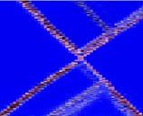
10 Single-hole transport in weakly coupled devices C)

11 Single-hole transport in weakly coupled devices Coulomb blockade conductance peaks C)
12 Low-temperature single-hole transport Excitation lines (Energy-level spacing of a few mev due to size confinement in the SiGe island)


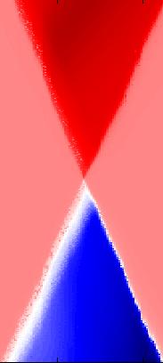
13 Zeeman splitting of quantum-dot hole states Direct tunneling spectroscopy G.K. et al., Nature Nanotechnology 5, 458 (2010)
14 Zeeman: Hz ~ -2kμ B B J Band Structure of SiGe g=6k g=2k g~0 g=4k Haendel et al., PRL 96, (2006) Composition dependent Luttinger parameter k: Ge: Si: % Ge: %Ge Fraj et al., Semiconductor Science and Technology 23, (2008). Fraj et al., J. Appl. Phys. 102, (2007).
15 Zeeman: Hz ~ -2kμ B B J Band Structure of SiGe g=6k g=2k g~0 g=4k Haendel et al., PRL 96, (2006) Composition dependent Luttinger parameter k: Ge: Si: % Ge: %Ge Fraj et al., Semiconductor Science and Technology 23, (2008). Fraj et al., J. Appl. Phys. 102, (2007). Nenashev et al., Phys. Rev. B 67, (2003)
16 Sequential Spin filling V sd 8 T 7 T 6 T 5 T N+1 N N-1 V g
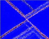
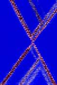
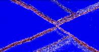
17 Sequential Spin filling V sd 8 T 7 T 6 T 5 T N+1 N N-1 V g 8 T 7 T 6 T 5 T
18 Inelastic cotunneling (strong coupling) Can be used for spectroscopy [De Franceschi et al, PRL 86, 878 (2001)] Resolution determined by temperature and not by life-time broadening! Flat featurelless differential conductance within coulomb diamond
19 Inelastic cotunneling (strong coupling) Can be used for spectroscopy [De Franceschi et al, PRL 86, 878 (2001)] Resolution determined by temperature and not by life-time broadening! ev = δ δ V sd N+1 N N-1 V g Step in differential conductance
20 Zeeman splitting measured by spin flip inelastic cotunneling


21 Zeeman splitting measured by spin flip inelastic cotunneling
22 Summary of g-factor results


23 Measuring the spin-orbit coupling strength

24 Measuring the spin-orbit coupling strength
25 Measuring the spin-orbit coupling strength

26 Measuring the spin-orbit coupling strength N. Roch et al., Nature 453, 633 (2008)
27 Measuring the spin-orbit coupling strength
28 Measuring the spin-orbit coupling strength
29 Measuring the spin-orbit coupling strength G. K. et al., Nature Nanotechnology 5, 458 (2010)

30 Measuring the spin-orbit coupling strength G. K. et al., Nature Nanotechnology 5, 458 (2010)


31 Summary First realization of three terminal devices based on SiGe self-assembled nanocrystals Low temperature measurements indicate strongly anisotropic hole g-factors Tunable spin-orbit coupling strength is demonstrated Outlook
QUANTUM TRANSPORT IN BOTTOM-UP SEMICONDUCTOR NANOSTRUCTURES
 QUANTUM TRANSPORT IN BOTTOM-UP SEMICONDUCTOR NANOSTRUCTURES Silvano De Franceschi INAC/SPSMS/LaTEQS: Laboratory of quantum electron transport and superconductivity http://www-drfmc.cea.fr/pisp/55/silvano.de_franceschi.html
GeSi Quantum Dot Superlattices
 GeSi Quantum Dot Superlattices ECE440 Nanoelectronics Zheng Yang Department of Electrical & Computer Engineering University of Illinois at Chicago Nanostructures & Dimensionality Bulk Quantum Walls Quantum
Influence of hyperfine interaction on optical orientation in self-assembled InAs/GaAs quantum dots
 Influence of hyperfine interaction on optical orientation in self-assembled InAs/GaAs quantum dots O. Krebs, B. Eble (PhD), S. Laurent (PhD), K. Kowalik (PhD) A. Kudelski, A. Lemaître, and P. Voisin Laboratoire
SUPPLEMENTARY INFORMATION
 Electrical control of single hole spins in nanowire quantum dots V. S. Pribiag, S. Nadj-Perge, S. M. Frolov, J. W. G. van den Berg, I. van Weperen., S. R. Plissard, E. P. A. M. Bakkers and L. P. Kouwenhoven
Lecture 8, April 12, 2017
 Lecture 8, April 12, 2017 This week (part 2): Semiconductor quantum dots for QIP Introduction to QDs Single spins for qubits Initialization Read-Out Single qubit gates Book on basics: Thomas Ihn, Semiconductor
Optical Characterization of Self-Assembled Si/SiGe Nano-Structures
 Optical Characterization of Self-Assembled Si/SiGe Nano-Structures T. Fromherz, W. Mac, G. Bauer Institut für Festkörper- u. Halbleiterphysik, Johannes Kepler Universität Linz, Altenbergerstraße 69, A-
Electrical Control of Single Spins in Semiconductor Quantum Dots Jason Petta Physics Department, Princeton University
 Electrical Control of Single Spins in Semiconductor Quantum Dots Jason Petta Physics Department, Princeton University g Q 2 m T + S Mirror U 3 U 1 U 2 U 3 Mirror Detector See Hanson et al., Rev. Mod. Phys.
Coulomb Blockade and Kondo Effect in Nanostructures
 Coulomb Blockade and Kondo Effect in Nanostructures Marcin M. Wysokioski 1,2 1 Institute of Physics Albert-Ludwigs-Universität Freiburg 2 Institute of Physics Jagiellonian University, Cracow, Poland 2.VI.2010
single-electron electron tunneling (SET)
") single-electron electron tunneling (SET) classical dots (SET islands): level spacing is NOT important; only the charging energy (=classical effect, many electrons on the island) quantum dots: : level spacing
single-electron electron tunneling (SET) classical dots (SET islands): level spacing is NOT important; only the charging energy (=classical effect, many electrons on the island) quantum dots: : level spacing
Electronic transport in low dimensional systems
 Electronic transport in low dimensional systems For example: 2D system l
Majorana single-charge transistor. Reinhold Egger Institut für Theoretische Physik
 Majorana single-charge transistor Reinhold Egger Institut für Theoretische Physik Overview Coulomb charging effects on quantum transport through Majorana nanowires: Two-terminal device: Majorana singlecharge
Surface Composition Mapping Of Semiconductor Quantum Dots. Stefan Heun, Laboratorio TASC INFM-CNR, Trieste, Italy.
 Surface Composition Mapping Of Semiconductor Quantum Dots Stefan Heun, Laboratorio TASC INFM-CNR, Trieste, Italy. Motivation Quantum Dot Applications based on their particular electronic properties (confinement)
Coherence and Correlations in Transport through Quantum Dots
 Coherence and Correlations in Transport through Quantum Dots Rolf J. Haug Abteilung Nanostrukturen Institut für Festkörperphysik and Laboratory for Nano and Quantum Engineering Gottfried Wilhelm Leibniz
Few-electron molecular states and their transitions in a single InAs quantum dot molecule
 Few-electron molecular states and their transitions in a single InAs quantum dot molecule T. Ota 1*, M. Rontani 2, S. Tarucha 1,3, Y. Nakata 4, H. Z. Song 4, T. Miyazawa 4, T. Usuki 4, M. Takatsu 4, and
Quantum Confinement in Graphene
 Quantum Confinement in Graphene from quasi-localization to chaotic billards MMM dominikus kölbl 13.10.08 1 / 27 Outline some facts about graphene quasibound states in graphene numerical calculation of
Zeeman splitting of single semiconductor impurities in resonant tunneling heterostructures
 Superlattices and Microstructures, Vol. 2, No. 4, 1996 Zeeman splitting of single semiconductor impurities in resonant tunneling heterostructures M. R. Deshpande, J. W. Sleight, M. A. Reed, R. G. Wheeler
interband transitions in semiconductors M. Fox, Optical Properties of Solids, Oxford Master Series in Condensed Matter Physics
 interband transitions in semiconductors M. Fox, Optical Properties of Solids, Oxford Master Series in Condensed Matter Physics interband transitions in quantum wells Atomic wavefunction of carriers in
Compositional mapping of semiconductor quantum dots by X-ray photoemission electron microscopy
 Compositional mapping of semiconductor quantum dots by X-ray photoemission electron microscopy Stefan Heun CNR-INFM, Italy, Laboratorio Nazionale TASC, Trieste and NEST-SNS, Pisa Outline A brief introduction
Electron counting with quantum dots
 Electron counting with quantum dots Klaus Ensslin Solid State Physics Zürich with S. Gustavsson I. Shorubalko R. Leturcq T. Ihn A. C. Gossard Time-resolved charge detection Single photon detection Time-resolved
Three-Dimensional Silicon-Germanium Nanostructures for Light Emitters and On-Chip Optical. Interconnects
 Three-Dimensional Silicon-Germanium Nanostructures for Light Emitters and On-Chip Optical eptember 2011 Interconnects Leonid Tsybeskov Department of Electrical and Computer Engineering New Jersey Institute
Surface compositional gradients of InAs/GaAs quantum dots
 Surface compositional gradients of InAs/GaAs quantum dots S. Heun, G. Biasiol, V. Grillo, E. Carlino, and L. Sorba Laboratorio Nazionale TASC INFM-CNR, I-34012 Trieste, Italy G. B. Golinelli University
Quantum Information Processing with Semiconductor Quantum Dots
 Quantum Information Processing with Semiconductor Quantum Dots slides courtesy of Lieven Vandersypen, TU Delft Can we access the quantum world at the level of single-particles? in a solid state environment?
Transport through Andreev Bound States in a Superconductor-Quantum Dot-Graphene System
 Transport through Andreev Bound States in a Superconductor-Quantum Dot-Graphene System Nadya Mason Travis Dirk, Yung-Fu Chen, Cesar Chialvo Taylor Hughes, Siddhartha Lal, Bruno Uchoa Paul Goldbart University
Three-terminal quantum-dot thermoelectrics
 Three-terminal quantum-dot thermoelectrics Björn Sothmann Université de Genève Collaborators: R. Sánchez, A. N. Jordan, M. Büttiker 5.11.2013 Outline Introduction Quantum dots and Coulomb blockade Quantum
Semiconductors: Applications in spintronics and quantum computation. Tatiana G. Rappoport Advanced Summer School Cinvestav 2005
 Semiconductors: Applications in spintronics and quantum computation Advanced Summer School 1 I. Background II. Spintronics Spin generation (magnetic semiconductors) Spin detection III. Spintronics - electron
Quantum Information Processing with Semiconductor Quantum Dots. slides courtesy of Lieven Vandersypen, TU Delft
 Quantum Information Processing with Semiconductor Quantum Dots slides courtesy of Lieven Vandersypen, TU Delft Can we access the quantum world at the level of single-particles? in a solid state environment?
Intraband emission of GaN quantum dots at λ =1.5 μm via resonant Raman scattering
 Intraband emission of GaN quantum dots at λ =1.5 μm via resonant Raman scattering L. Nevou, F. H. Julien, M. Tchernycheva, J. Mangeney Institut d Electronique Fondamentale, UMR CNRS 8622, University Paris-Sud
Concepts in Spin Electronics
 Concepts in Spin Electronics Edited by Sadamichi Maekawa Institutefor Materials Research, Tohoku University, Japan OXFORD UNIVERSITY PRESS Contents List of Contributors xiii 1 Optical phenomena in magnetic
Spectromicroscopic investigations of semiconductor quantum dots. Stefan Heun, Laboratorio TASC INFM-CNR, Trieste, Italy.
 Spectromicroscopic investigations of semiconductor quantum dots Stefan Heun, Laboratorio TASC INFM-CNR, Trieste, Italy. Motivation Quantum Dot Applications based on their particular electronic properties
Chapter 8: Coulomb blockade and Kondo physics
 Chater 8: Coulomb blockade and Kondo hysics 1) Chater 15 of Cuevas& Scheer. REFERENCES 2) Charge transort and single-electron effects in nanoscale systems, J.M. Thijssen and H.S.J. Van der Zant, Phys.
Formation of unintentional dots in small Si nanostructures
 Superlattices and Microstructures, Vol. 28, No. 5/6, 2000 doi:10.1006/spmi.2000.0942 Available online at http://www.idealibrary.com on Formation of unintentional dots in small Si nanostructures L. P. ROKHINSON,
Chapter 3. Step Structures and Epitaxy on Semiconductor Surfaces
 and Epitaxy on Semiconductor Surfaces Academic and Research Staff Professor Simon G.J. Mochrie, Dr. Ophelia Tsui Graduate Students Seugheon Song, Mirang Yoon 3.1 Introduction Sponsors Joint Services Electronics
Precise control of size and density of self-assembled Ge dot on Si(1 0 0) by carbon-induced strain-engineering
 by carbon-induced strain-engineering") Applied Surface Science 216 (2003) 419 423 Precise control of size and density of self-assembled Ge dot on Si(1 0 0) by carbon-induced strain-engineering Y. Wakayama a,*, L.V. Sokolov b, N. Zakharov c,
Applied Surface Science 216 (2003) 419 423 Precise control of size and density of self-assembled Ge dot on Si(1 0 0) by carbon-induced strain-engineering Y. Wakayama a,*, L.V. Sokolov b, N. Zakharov c,
Manipulation of Majorana fermions via single charge control
 Manipulation of Majorana fermions via single charge control Karsten Flensberg Niels Bohr Institute University of Copenhagen Superconducting hybrids: from conventional to exotic, Villard de Lans, France,
SUPPLEMENTARY INFORMATION
 Supramolecular Spin Valves M. Urdampilleta, 1 J.-P. Cleuziou, 1 S. Klyatskaya, 2 M. Ruben, 2,3* W. Wernsdorfer 1,* 1 Institut Néel, associé á l Université Joseph Fourier, CNRS, BP 166, 38042 Grenoble Cedex
Monolithic growth of ultra-thin Ge nanowires on Si(001)
") Monolithic growth of ultra-thin Ge nanowires on Si(001) J. J. Zhang, 1 * G. Katsaros, 1, F. Montalenti, 2 D. Scopece, 2 R. O. Rezaev, 1,4 C. Mickel, 1 B. Rellinghaus, 1 L. Miglio, 2 S. De Franceschi, 3
Monolithic growth of ultra-thin Ge nanowires on Si(001) J. J. Zhang, 1 * G. Katsaros, 1, F. Montalenti, 2 D. Scopece, 2 R. O. Rezaev, 1,4 C. Mickel, 1 B. Rellinghaus, 1 L. Miglio, 2 S. De Franceschi, 3
Lecture 2: Double quantum dots
 Lecture 2: Double quantum dots Basics Pauli blockade Spin initialization and readout in double dots Spin relaxation in double quantum dots Quick Review Quantum dot Single spin qubit 1 Qubit states: 450
Energy dispersion relations for holes inn silicon quantum wells and quantum wires
 Purdue University Purdue e-pubs Other Nanotechnology Publications Birck Nanotechnology Center 6--7 Energy dispersion relations for holes inn silicon quantum wells and quantum wires Vladimir Mitin Nizami
Coulomb blockade and single electron tunnelling
 Coulomb blockade and single electron tunnelling Andrea Donarini Institute of theoretical physics, University of Regensburg Three terminal device Source System Drain Gate Variation of the electrostatic
Nuclear spin spectroscopy for semiconductor hetero and nano structures
 (Interaction and Nanostructural Effects in Low-Dimensional Systems) November 16th, Kyoto, Japan Nuclear spin spectroscopy for semiconductor hetero and nano structures Yoshiro Hirayama Tohoku University
Herre van der Zant. interplay between molecular spin and electron transport (molecular spintronics) Gate
 Gate") transport through the single molecule magnet Mn12 Herre van der Zant H.B. Heersche, Z. de Groot (Delft) C. Romeike, M. Wegewijs (RWTH Aachen) D. Barreca, E. Tondello (Padova) L. Zobbi, A. Cornia (Modena)
transport through the single molecule magnet Mn12 Herre van der Zant H.B. Heersche, Z. de Groot (Delft) C. Romeike, M. Wegewijs (RWTH Aachen) D. Barreca, E. Tondello (Padova) L. Zobbi, A. Cornia (Modena)
Cotunneling and Kondo effect in quantum dots. Part I/II
 & NSC Cotunneling and Kondo effect in quantum dots Part I/II Jens Paaske The Niels Bohr Institute & Nano-Science Center Bad Honnef, September, 2010 Dias 1 Lecture plan Part I 1. Basics of Coulomb blockade
Determination of the tunnel rates through a few-electron quantum dot
 Determination of the tunnel rates through a few-electron quantum dot R. Hanson 1,I.T.Vink 1, D.P. DiVincenzo 2, L.M.K. Vandersypen 1, J.M. Elzerman 1, L.H. Willems van Beveren 1 and L.P. Kouwenhoven 1
Electroluminescence from Silicon and Germanium Nanostructures
 Electroluminescence from silicon Silicon Getnet M. and Ghoshal S.K 35 ORIGINAL ARTICLE Electroluminescence from Silicon and Germanium Nanostructures Getnet Melese* and Ghoshal S. K.** Abstract Silicon
Resonantly Excited Time-Resolved Photoluminescence Study of Self-Organized InGaAs/GaAs Quantum Dots
 R. Heitz et al.: PL Study of Self-Organized InGaAs/GaAs Quantum Dots 65 phys. stat. sol. b) 221, 65 2000) Subject classification: 73.61.Ey; 78.47.+p; 78.55.Cr; 78.66.Fd; S7.12 Resonantly Excited Time-Resolved
Lecture contents. Stress and strain Deformation potential. NNSE 618 Lecture #23
 1 Lecture contents Stress and strain Deformation potential Few concepts from linear elasticity theory : Stress and Strain 6 independent components 2 Stress = force/area ( 3x3 symmetric tensor! ) ij ji
Band-edge alignment of SiGe/ Si quantum wells and SiGe/ Si self-assembled islands
 Band-edge alignment of SiGe/ Si quantum wells and SiGe/ Si self-assembled islands M. El Kurdi,* S. Sauvage, G. Fishman, and P. Boucaud Institut d Électronique Fondamentale, UMR CNRS 8622, Bâtiment 220,
Since first discovered in 1990, 1 heteroepitaxially grown selfassembled
 pubs.acs.org/nanolett Thermodynamic Self-Limiting Growth of Heteroepitaxial Islands Induced by Nonlinear Elastic Effect Hao Hu, Xiaobin Niu, and Feng Liu*,, Frontier Institute of Science and Technology,
Widely Tunable and Intense Mid-Infrared PL Emission from Epitaxial Pb(Sr)Te Quantum Dots in a CdTe Matrix
Te Quantum Dots in a CdTe Matrix") Widely Tunable and Intense Mid-Infrared PL Emission from Epitaxial Pb(Sr)Te Quantum Dots in a Matrix S. Kriechbaumer 1, T. Schwarzl 1, H. Groiss 1, W. Heiss 1, F. Schäffler 1,T. Wojtowicz 2, K. Koike 3,
Widely Tunable and Intense Mid-Infrared PL Emission from Epitaxial Pb(Sr)Te Quantum Dots in a Matrix S. Kriechbaumer 1, T. Schwarzl 1, H. Groiss 1, W. Heiss 1, F. Schäffler 1,T. Wojtowicz 2, K. Koike 3,
Heavy hole states in Germanium hut wires
 Heavy hole states in Germanium hut wires arxiv:1607.0977v1 [cond-mat.mes-hall] 11 Jul 016 Hannes Watzinger,,, Christoph Kloeffel,, Lada Vukušić,, Marta D. Rossell,, Violetta Sessi, Josip Kukučka,, Raimund
Single photon emitters in exfoliated WSe 2 structures
 Single photon emitters in exfoliated WSe 2 structures M. Koperski, 1,2 K. Nogajewski, 1 A. Arora, 1 V. Cherkez, 3 P. Mallet, 3 J.-Y. Veuillen, 3 J. Marcus, 3 P. Kossacki, 1,2 and M. Potemski 1 1 Laboratoire
Semiconductor Quantum Dots
 Semiconductor Quantum Dots M. Hallermann Semiconductor Physics and Nanoscience St. Petersburg JASS 2005 Outline Introduction Fabrication Experiments Applications Porous Silicon II-VI Quantum Dots III-V
g-factors in quantum dots
 g-factors in quantum dots Craig Pryor Dept. of Physics and Astronomy University of Iowa With: Michael Flatté, Joseph Pingenot, Amrit De supported by DARPA/ARO DAAD19-01-1-0490 g-factors in quantum dots
Raman spectroscopy of self-assembled InAs quantum dots in wide-bandgap matrices of AlAs and aluminium oxide
 Mat. Res. Soc. Symp. Proc. Vol. 737 2003 Materials Research Society E13.8.1 Raman spectroscopy of self-assembled InAs quantum dots in wide-bandgap matrices of AlAs and aluminium oxide D. A. Tenne, A. G.
Lectures: Condensed Matter II 1 Electronic Transport in Quantum dots 2 Kondo effect: Intro/theory. 3 Kondo effect in nanostructures
 Lectures: Condensed Matter II 1 Electronic Transport in Quantum dots 2 Kondo effect: Intro/theory. 3 Kondo effect in nanostructures Luis Dias UT/ORNL Lectures: Condensed Matter II 1 Electronic Transport
Quantum physics in quantum dots
 Quantum physics in quantum dots Klaus Ensslin Solid State Physics Zürich AFM nanolithography Multi-terminal tunneling Rings and dots Time-resolved charge detection Moore s Law Transistors per chip 10 9
InAs quantum dots: Predicted electronic structure of free-standing versus GaAs-embedded structures
 PHYSICAL REVIEW B VOLUME 59, NUMBER 24 15 JUNE 1999-II InAs quantum dots: Predicted electronic structure of free-standing versus GaAs-embedded structures A. J. Williamson and Alex Zunger National Renewable
Supplementary Information for Pseudospin Resolved Transport Spectroscopy of the Kondo Effect in a Double Quantum Dot. D2 V exc I
 Supplementary Information for Pseudospin Resolved Transport Spectroscopy of the Kondo Effect in a Double Quantum Dot S. Amasha, 1 A. J. Keller, 1 I. G. Rau, 2, A. Carmi, 3 J. A. Katine, 4 H. Shtrikman,
From nanophysics research labs to cell phones. Dr. András Halbritter Department of Physics associate professor
 From nanophysics research labs to cell phones Dr. András Halbritter Department of Physics associate professor Curriculum Vitae Birth: 1976. High-school graduation: 1994. Master degree: 1999. PhD: 2003.
Physics and Material Science of Semiconductor Nanostructures
 Physics and Material Science of Semiconductor Nanostructures PHYS 570P Prof. Oana Malis Email: omalis@purdue.edu Course website: http://www.physics.purdue.edu/academic_programs/courses/phys570p/ 1 Introduction
X-ray Absorption studies of atomic environments in semiconductor nanostructures
 X-ray Absorption studies of atomic environments in semiconductor nanostructures Federico Boscherini and Department of Physics, Italy Introduction Why XAS for nanostructures How XAS for nanostructures Interdiffusion
Single Electron Transistor (SET)
") Single Electron Transistor (SET) SET: e - e - dot A single electron transistor is similar to a normal transistor (below), except 1) the channel is replaced by a small dot. C g 2) the dot is separated from
Single Electron Transistor (SET) SET: e - e - dot A single electron transistor is similar to a normal transistor (below), except 1) the channel is replaced by a small dot. C g 2) the dot is separated from
Bruit de grenaille mesuré par comptage d'électrons dans une boîte quantique
 Bruit de grenaille mesuré par comptage d'électrons dans une boîte quantique GDR Physique Quantique Mésoscopique, Aussois, 19-22 mars 2007 Simon Gustavsson Matthias Studer Renaud Leturcq Barbara Simovic
Large Storage Window in a-sinx/nc-si/a-sinx Sandwiched Structure
 2017 Asia-Pacific Engineering and Technology Conference (APETC 2017) ISBN: 978-1-60595-443-1 Large Storage Window in a-sinx/nc-si/a-sinx Sandwiched Structure Xiang Wang and Chao Song ABSTRACT The a-sin
Kondo effect in multi-level and multi-valley quantum dots. Mikio Eto Faculty of Science and Technology, Keio University, Japan
 Kondo effect in multi-level and multi-valley quantum dots Mikio Eto Faculty of Science and Technology, Keio University, Japan Outline 1. Introduction: next three slides for quantum dots 2. Kondo effect
Effect of wetting layers on the strain and electronic structure of InAs self-assembled quantum dots
 Purdue University Purdue e-pubs Birck and NCN Publications Birck Nanotechnology Center February 2008 Effect of wetting layers on the strain and electronic structure of InAs self-assembled quantum dots
Deterministic Coherent Writing and Control of the Dark Exciton Spin using Short Single Optical Pulses
 Deterministic Coherent Writing and Control of the Dark Exciton Spin using Short Single Optical Pulses Ido Schwartz, Dan Cogan, Emma Schmidgall, Liron Gantz, Yaroslav Don and David Gershoni The Physics
We study spin correlation in a double quantum dot containing a few electrons in each dot ( 10). Clear
. Clear") Pauli spin blockade in cotunneling transport through a double quantum dot H. W. Liu, 1,,3 T. Fujisawa, 1,4 T. Hayashi, 1 and Y. Hirayama 1, 1 NTT Basic Research Laboratories, NTT Corporation, 3-1 Morinosato-Wakamiya,
Pauli spin blockade in cotunneling transport through a double quantum dot H. W. Liu, 1,,3 T. Fujisawa, 1,4 T. Hayashi, 1 and Y. Hirayama 1, 1 NTT Basic Research Laboratories, NTT Corporation, 3-1 Morinosato-Wakamiya,
solidi current topics in solid state physics InAs quantum dots grown by molecular beam epitaxy on GaAs (211)B polar substrates
B polar substrates") solidi status physica pss c current topics in solid state physics InAs quantum dots grown by molecular beam epitaxy on GaAs (211)B polar substrates M. Zervos1, C. Xenogianni1,2, G. Deligeorgis1, M. Androulidaki1,
solidi status physica pss c current topics in solid state physics InAs quantum dots grown by molecular beam epitaxy on GaAs (211)B polar substrates M. Zervos1, C. Xenogianni1,2, G. Deligeorgis1, M. Androulidaki1,
Morphological evolution of single-crystal ultrathin solid films
 Western Kentucky University From the SelectedWorks of Mikhail Khenner March 29, 2010 Morphological evolution of single-crystal ultrathin solid films Mikhail Khenner, Western Kentucky University Available
ASINGLE-ELECTRON memory is an ultimate device
 IEEE TRANSACTIONS ON NANOTECHNOLOGY, VOL. 5, NO. 1, JANUARY 2006 37 Simulation of a Ge Si Hetero-Nanocrystal Memory Dengtao Zhao, Member, IEEE, Yan Zhu, Ruigang Li, Senior Member, IEEE, and Jianlin Liu,
Defense Technical Information Center Compilation Part Notice
 UNCLASSIFIED Defense Technical Information Center Compilation Part Notice ADP013124 TITLE: Resonant Acceptors States in Ge/Ge[1-x]Si[x] MQW Hetero structures DISTRIBUTION: Approved for public release,
Spectroscopy of self-assembled quantum rings
 Spectroscopy of self-assembled quantum rings RJWarburton 1, B Urbaszek 1,EJMcGhee 1,CSchulhauser 2, A Högele 2, K Karrai 2, A O Govorov 3,JABarker 4, B D Gerardot 5,PMPetroff 5,and JMGarcia 6 1 Department
Quantum Dots: Artificial Atoms & Molecules in the Solid-State
 Network for Computational Nanotechnology (NCN) Purdue, Norfolk State, Northwestern, UC Berkeley, Univ. of Illinois, UTEP Quantum Dots: Artificial Atoms & Molecules in the Solid-State Network for Computational
Hole Spin Relaxation in Ge- Si Core-Shell Nanowire Qubits
 Hole Spin Relaxation in Ge- Si Core-Shell Nanowire Qubits The Harvard community has made this article openly available. Please share how this access benefits you. Your story matters Citation Hu, Yongjie,
Introduction to semiconductor nanostructures. Peter Kratzer Modern Concepts in Theoretical Physics: Part II Lecture Notes
 Introduction to semiconductor nanostructures Peter Kratzer Modern Concepts in Theoretical Physics: Part II Lecture Notes What is a semiconductor? The Fermi level (chemical potential of the electrons) falls
Spins and spin-orbit coupling in semiconductors, metals, and nanostructures
 B. Halperin Spin lecture 1 Spins and spin-orbit coupling in semiconductors, metals, and nanostructures Behavior of non-equilibrium spin populations. Spin relaxation and spin transport. How does one produce
Electronic and Optoelectronic Properties of Semiconductor Structures
 Electronic and Optoelectronic Properties of Semiconductor Structures Jasprit Singh University of Michigan, Ann Arbor CAMBRIDGE UNIVERSITY PRESS CONTENTS PREFACE INTRODUCTION xiii xiv 1.1 SURVEY OF ADVANCES
Coulomb blockade in metallic islands and quantum dots
 Coulomb blockade in metallic islands and quantum dots Charging energy and chemical potential of a metallic island Coulomb blockade and single-electron transistors Quantum dots and the constant interaction
Chapter 3 Properties of Nanostructures
 Chapter 3 Properties of Nanostructures In Chapter 2, the reduction of the extent of a solid in one or more dimensions was shown to lead to a dramatic alteration of the overall behavior of the solids. Generally,
Pseudopotential Theory of Semiconductor Quantum Dots
 phys. stat. sol. (b) 224, No. 3, 727 734 (2001) Pseudopotential Theory of Semiconductor Quantum Dots Alex Zunger National Renewable Energy Laboratory, Golden, CO 80401, USA (Received July 31, 2000; accepted
SUPPLEMENTARY INFORMATION
 SUPPLEMENTARY INFORMATION DOI: 10.1038/NNANO.2014.16 Electrical detection of charge current-induced spin polarization due to spin-momentum locking in Bi 2 Se 3 by C.H. Li, O.M.J. van t Erve, J.T. Robinson,
Wave function engineering in quantum dot-ring structures
 Wave function engineering in quantum dot-ring structures Nanostructures with highly controllable electronic properties E. Zipper, M. Kurpas, M. M. Maśka Instytut Fizyki, Uniwersytet Sląski w Katowicach,
Christian Ratsch, UCLA
 Strain Dependence of Microscopic Parameters and its Effects on Ordering during Epitaxial Growth Christian Ratsch, UCLA Institute for Pure and Applied Mathematics, and Department of Mathematics Collaborators:
Introduction. Resonant Cooling of Nuclear Spins in Quantum Dots
 Introduction Resonant Cooling of Nuclear Spins in Quantum Dots Mark Rudner Massachusetts Institute of Technology For related details see: M. S. Rudner and L. S. Levitov, Phys. Rev. Lett. 99, 036602 (2007);
Optical Spectroscopies of Thin Films and Interfaces. Dietrich R. T. Zahn Institut für Physik, Technische Universität Chemnitz, Germany
 Optical Spectroscopies of Thin Films and Interfaces Dietrich R. T. Zahn Institut für Physik, Technische Universität Chemnitz, Germany 1. Introduction 2. Vibrational Spectroscopies (Raman and Infrared)
Self-Assembled InAs Quantum Dots
 Self-Assembled InAs Quantum Dots Steve Lyon Department of Electrical Engineering What are semiconductors What are semiconductor quantum dots How do we make (grow) InAs dots What are some of the properties
tunneling theory of few interacting atoms in a trap
 tunneling theory of few interacting atoms in a trap Massimo Rontani CNR-NANO Research Center S3, Modena, Italy www.nano.cnr.it Pino D Amico, Andrea Secchi, Elisa Molinari G. Maruccio, M. Janson, C. Meyer,
Temperature dependence of Andreev spectra in a superconducting carbon nanotube quantum dot
 Temperature dependence of Andreev spectra in a superconducting carbon nanotube quantum dot A. Kumar, M. Gaim, D. Steininger, A. Levy Yeyati, A. Martín-Rodero, A. K. Hüttel, and C. Strunk Phys. Rev. B 89,
How a single defect can affect silicon nano-devices. Ted Thorbeck
 How a single defect can affect silicon nano-devices Ted Thorbeck tedt@nist.gov The Big Idea As MOS-FETs continue to shrink, single atomic scale defects are beginning to affect device performance Gate Source
Nanoscience, MCC026 2nd quarter, fall Quantum Transport, Lecture 1/2. Tomas Löfwander Applied Quantum Physics Lab
 Nanoscience, MCC026 2nd quarter, fall 2012 Quantum Transport, Lecture 1/2 Tomas Löfwander Applied Quantum Physics Lab Quantum Transport Nanoscience: Quantum transport: control and making of useful things
PACS numbers: La, Dx Keywords: A. Semiconductors; A. Nanostructures; D. Electronic states
 Title: Exact calculation of single-electron states in Si-nanocrystal embedded in SiO Authors: Nguyen Hong Quang a,b, Tran The Trung a,c, Johann Sée b and Philippe Dollfus b, a Institute of Physics, NCST,
Single Electron Tunneling Examples
 Single Electron Tunneling Examples Danny Porath 2002 (Schönenberger et. al.) It has long been an axiom of mine that the little things are infinitely the most important Sir Arthur Conan Doyle Books and
Nanomaterials and Analytics Semiconductor Nanocrystals and Carbon Nanotubes. - Introduction and Preparation - Characterisation - Applications
 Nanomaterials and Analytics Semiconductor Nanocrystals and Carbon Nanotubes - Introduction and Preparation - Characterisation - Applications Dietrich RT Zahn Semiconductor Physics,, TU Chemnitz http://www.tu-chemnitz.de/physik/hlph/
Supporting Information
 Electronic Supplementary Material (ESI) for Nanoscale. This journal is The Royal Society of Chemistry 2015 Supporting Information Single Layer Lead Iodide: Computational Exploration of Structural, Electronic
Lecture 3: Heterostructures, Quasielectric Fields, and Quantum Structures
 Lecture 3: Heterostructures, Quasielectric Fields, and Quantum Structures MSE 6001, Semiconductor Materials Lectures Fall 2006 3 Semiconductor Heterostructures A semiconductor crystal made out of more
collaboration D. G. Austing (NTT BRL, moved to NRC) Y. Tokura (NTT BRL) Y. Hirayama (NTT BRL, CREST-JST) S. Tarucha (Univ. of Tokyo, NTT BRL,
 Y. Tokura (NTT BRL) Y. Hirayama (NTT BRL, CREST-JST) S. Tarucha (Univ. of Tokyo, NTT BRL,") This is the viewgraph with the recorded talk at the 26th International Conference on Physics of Semiconductor (ICPS26, Edinburgh, 22). By clicking the upper-left button in each page, you can hear the talk
This is the viewgraph with the recorded talk at the 26th International Conference on Physics of Semiconductor (ICPS26, Edinburgh, 22). By clicking the upper-left button in each page, you can hear the talk
Ordering of Nanostructures in a Si/Ge 0.3 Si 0.7 /Ge System during Molecular Beam Epitaxy
 Semiconductors, Vol. 36, No. 11, 22, pp. 1294 1298. Translated from Fizika i Tekhnika Poluprovodnikov, Vol. 36, No. 11, 22, pp. 1379 1383. Original Russian Text Copyright 22 by Cirlin, Egorov, Sokolov,
Final exam. Introduction to Nanotechnology. Name: Student number:
 1 Final exam. Introduction to Nanotechnology Name: Student number: 1. (a) What is the definition for a cluster size-wise? (3%) (b) Calculate the energy separation near the Fermi surface of a metallic cluster
Enhancement-mode quantum transistors for single electron spin
 Purdue University Purdue e-pubs Other Nanotechnology Publications Birck Nanotechnology Center 8-1-2006 Enhancement-mode quantum transistors for single electron spin G. M. Jones B. H. Hu C. H. Yang M. J.