Single Electron Tunneling Examples
|
|
|
- Silvester Richards
- 6 years ago
- Views:
Transcription
 It has long been an axiom of mine that the little things are infinitely the most important")
1 Single Electron Tunneling Examples Danny Porath 2002 (Schönenberger et. al.) It has long been an axiom of mine that the little things are infinitely the most important Sir Arthur Conan Doyle
2 Books and Internet Sites Electronic Transport in Mesoscopic Systems, S. Datta Single Charge Tunneling, H. Grabert & M.H. Devoret Introduction to Mesoscopic Physics, Y. Imry ttp://
3 1.Read the paper: Homework 8 Variation of the Coulomb staircase in a two-junction system by fractional electron charge, by: M.E. Hanna and M. Tinkham, Physical Review B, 44(11), 5919 (1991).
4 Outline SET Examples: 1. The C 60 work D.P. et. al. a. Background b. Sample preparation and imaging c. SET Theory d. I-V Spectroscopy results and fits e. Summary (of this part) 2. Advanced material from C. Schönenberger a. Introduction b. Law transparency SET c. High transparency Fabry Perot & UCF d. Intermediate transparency Co-tunneling & Kondo e. Conclusions (from this part)

5 Single Electron Tunneling and Level Spectroscopy of Single C 60 Molecules Danny Porath, Muin Tarabia, Yair Levi and Oded Millo
6 The General Experimental Scheme I R 1,C 1 V QD C 60 Insulating layer STM tip J-1 J-2 R 2,C 2 gold

7 C 60 Fullerenes Structure: (icosahedral symmetry) : 1,000,000,000 ~1 m ~10 Å 60 carbon atoms. (20 hexagons, 12 pentagons)
8 Bacground Before... Significant effort was devoted to studies of the interplay between Single Electron Tunneling (SET) effects and quantum size effects in isolated nanoparticles. The interplay was studied for: E l << E c (Tinkham, Van-Kempen, Sivan, Molenkamp) C 60 spectroscopy was done mainly by optical means, limited by selection rules.
9 Background What was new here? Extremely small QD (~8 Å) Quantum Size effects even at RT. Interplay between SET and discrete levels in two regimes: E c < E l E c > E l Tunneling spectroscopy of isolated C 60 Electronic level splitting.
 a PMMA layer Gold substrate Prepared sample C 60")
10 Steps: Sample Preparation Rinse C 60 powder in Toluene Evaporate dried powder on a gold substrate covered by carbon and (later) a PMMA layer Gold substrate Prepared sample C 60 Evaporation

11 100 Å 50 Å STM Images of C 60 Fullerenes 70 Å 40 Å

12 STM Images of C 60 Fullerenes 3-D
13 SET Effects in DBTJ I I-V curves CB V Q D R 1,C 1 R 2,C 2 STM tip Tunnel Junction 1 Tunnel Junction 2 I T (V) CS SET effects can be observed If: 1) E C = e 2 /2C > k B T Charging Energy > Thermal Energy 2) R T > R Q = h/e 2 Tunneling Resistance > Quantum Resistance Coulomb Blockade (CB): I T = 0 up to V t e/2c ; V t depends on fractional charge Q 0 Coulomb Staircase (CS): Sequence of steps in I-V. Each step - adding an electron to the island V
14 Charge Quantization Leads to SET Effects Charge quantization leads to SET effects: V t depends on fractional charge Q 0. Q 0 represents any offset potentials. Q = ne - Q 0 ; Q 0 e/2 E Q 0 = Q(e) 2 E c Q 0 = e/2-1 E 0 1 Q(e) V t = e/2c V t = 0 2 Allowed states with n access electrons indicated on the graphs
15 Origin of the Fractional Charge Q 0 Difference in contact potentials across the junctions: Q 0 = (C 1 φ 1 -C 2 φ 2 )/e Note: We are interested only in Q 0 mod e. Q 0 can be varied by controlling C 1 through tipsample separation. This is done by changing the STM current and bias settings.
16 Interplay Between SET Effects and Discrete Energy Levels E L << E C : (Level Spacing << Charging Energy) e No levels E c E L << E C 1 2 (Amman et al.) Additional sub-steps on top of a CS step
17 Interplay Between SET Effects and Discrete Energy Levels E L ~ E C : (Level Spacing ~ Charging Energy) CS steps are no more equidistantly spaced. zero bias gap is not suppressed for Q 0 = e/2 when the CB is suppressed. Pronounced asymmetry of I-V curves due to different levels on each side.
18 I-V Measurements V I Q R 1,C 1 R 2,C 2 STM tip 1 2 Tunneling Current [na] Single molecule T = 4.2 K (a) 0 (b) Tip-Bias [V] Tunneling Current [na] Single molecule T = 300 K (c) Tip-Bias [V] Tunneling Current [na] Two molecules T = 300 K (d) T = 4.2 K Tip Bias [V] I-V measurements are done while disconnecting the feed-back loop. Note: 1. Non-vanishing gap. 2. Pronounced asymmetry and different steps.
19 I-V Measurements di/dv (a.u.) di/dv (a.u.) di/dv (a.u.) I (na) Tip Voltage (V) Tip Voltage (V) T = 4.2 K (a) (b) (c) T = 4.2 K T = 300 K di/dv Tip Voltage (V)
20 HOMO+1 (?) di/dv LUMO+1 LUMO E F HOMO Tip Voltage (V) Tunneling through LUMO+1 Tunneling through LUMO
21 Local Fields (Sarid et. al.) Different electric fields (carbon field, STM tip) effect the molecular orbitals differently (Stark effect).
22 Molecule Orientation (Guntherodt et. al.) Tunneling channel (depending on the molecule orientation) effects the level splitting.
23 Jahn - Teller effect (Bendale et. al.) A splitting or a shift of the energy levels due to structural distortion. The C 60+ h u reduces by ~ 0.6 ev
24 Theoretical Fits (Orthodox theory-averin & Likharev) Schematic of the circuit: R 1,C 1 R QD 2,C 2 I V The tunneling rate on the dot: ± i (n) = 2π h T(E) i 2 D (E i E )f(e i E )D i d (E E d )[1 f(e E d )]de Γ i± (n) - Tunneling rate to/from the dot from/to the electrode. f - Fermi function. D i (E), E i - DOS/Fermi energy at electrode i. D d (E), E d - DOS/Fermi energy at the dot. T i (E) - Tunneling matrix element.
25 Theoretical Fits (Orthodox theory-averin & Likharev) We choose the density of states D d (E): The tunneling current is: + I(V) = e P(n)[Γ2 (n) Γ2 (n)] = e P(n)[Γ1 (n) Γ1 + (n)] P(n) The probability to find n electrons on the dot
26 Energy Level Calculations
27 xperimental Results Asymmetrical Curves 9 (a) Exp. 9 (b) Exp. Tunneling Current [na] Fits di/dv [a.u.] Fits Bias [V] Bias [V] 1.6 C 1 ~ C 2 ~ 10-19, E HOMO -E LUMO ~ 0.7 ev, E L ~ 0.05 ev
28 Source of Asymmetry C 1 <C 2 ==> V 1 >V 2 ==> Onset of tunneling at junction 1 (for the level configuration at hand) Positive bias Negative bias
29 Experimental Results Symmetrical Curves 4 (a) 3 Exp. 3 2 (b) Exp. Tunneling Current [na] Fits di/dv [a.u.] Fits Bias [V] Bias [V] C 1 ~ C 2 ~ 10-19, E HOMO -E LUMO ~ 0.7 ev, E L ~ 0.05 ev
30 Symmetrical Barriers (C 1 ~C 2 ) Positive bias Negative bias Tunneling through the set of levels closer to E F -in our case the 3 LUMO levels.
31 Checking The Model - Experimentally Tunneling Current (na) Tunneling Current (na) C 1 < C 2 I s = 1.6 na V s = 0.75 V A C 1 > C 2 I s = 6 na V s = 0.75 V B di/dv (a.u.) di/dv (a.u.) Tip Voltage (V)
32 The Triple Barrier Tunnel Junction (TBTJ) V I QD QD R 1,C 1 R 2,C 2 R 3,C 3 Note: PMMA STM tip C 60 J-1 J-2 C J-3 Non Vanishing gap. gold Tunneling Current [na] Two molecules T = 300 K Negative differential resistance (NDR) T = 4.2 K Tip Bias [V] Non-ohmic curves everywhere on the sample.
33 Summary - C 60 STM Spectroscopy A C 60 molecule is an ideal quantum dot for studies of single electron tunneling and quantum size effects. The interplay between SET effects and molecular levels is clearly observed at 4.2 K as well as at RT for the double barrier tunnel junction configuration. The degeneracy of the HOMO, LUMO and LUMO+1 levels was fully resolved, and the degree of splitting is consistent with the J-T effect.
34 Quantum Dot Physics C. Schönenberger

35 Quantum dots
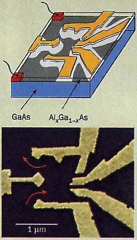
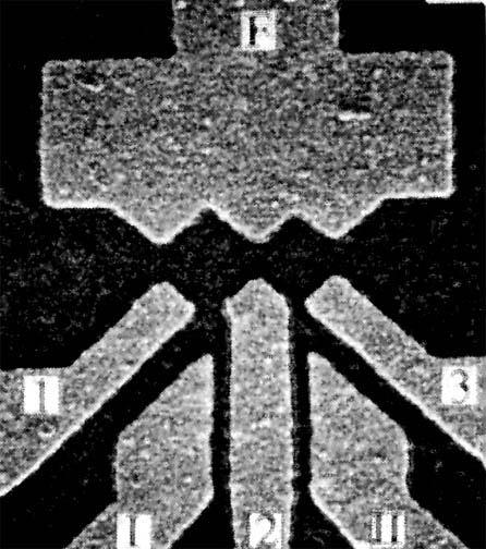
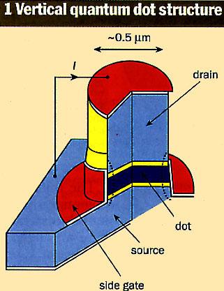
36 ( conventional ) Quantum dots planar dot planar double-dot vertical dot

37 quantum dot? 2 µm
 δe=h/τ round-trip in addition: ev and kt example: 0d with respect to")
38 Different energies (what is 0d?) δe=h/τ round-trip in addition: ev and kt example: 0d with respect to quantum-size effects, provided: kt, ev, and Γ < δe
39 Contacts matter...!. low transparency single-electron tunneling determined by single-electron charging effects, e.g. Coulomb blockade (0d limit). intermediate transparency charging effects but co-tunneling, e.g. Kondo effect. high transparency quantum interference of non-interacting electrons, e.g. Fabry-Perot resonances and UCF (disordered limit)
40 Contacts matter...!. low transparency single-electron tunneling determined by single-electron charging effects, e.g. Coulomb blockade (0d limit)
 here: black = low differential conductance Coulomb")
41 Single-electron tunneling greyscale plot of di/dv (V gate,v bias ) here: black = low differential conductance Coulomb blockade
 E add add")


42 tutorial on di/dv plots V sd (mv) E add add addition energy, i.e. sum of: single-electron charging energy U C V g level-spacing δe Change V sd Change V g


43 even even even odd odd odd filling of states according to S = 1/2 0 1/2... odd number of electrons: Ε add = UC even number of electrons: Ε add = UC + δe
44 single-electron-tunneling if tunneling probability p of each junction is small : current determined by accessible levels in dot i.e. by level spacing and Coulomb charging energy uncorrelated sequential tunneling dominates. Current I p
45 Contacts matter...!. low transparency single-electron tunneling determined by single-electron charging effects, e.g. Coulomb blockade (0d limit). intermediate transparency charging effects but co-tunneling, e.g. Kondo effect. high transparency quantum interference of non-interacting electrons, e.g. Fabry-Perot resonances and UCF (disordered limit)

46 T~1 limit (interaction-free wire) bias voltage 5 mv -5 mv gate voltage V
 round-trip phase depends on E I V = e 2 { T ( ev / 2) + T ( ev / 2)")
47 T~1 limit (wire) T ( E) = 2 1+ R C + TC 2R cos( Θ + C 2δ R ) Θ = L( k + k ) round-trip phase depends on E I V = e 2 { T ( ev / 2) + T ( ev / 2) }

48 Fabry-Perot (interference) 5 mv -5 mv their data gate voltage V simple model
49 Contacts matter...!. low transparency single-electron tunneling determined by single-electron charging effects, e.g. Coulomb blockade (0d limit). intermediate transparency charging effects but co-tunneling, e.g. Kondo effect. high transparency quantum interference of non-interacting electrons, e.g. Fabry-Perot resonances and UCF (disordered limit)

 order processes add")
50 co-tunneling if tunneling probability p of each junction is large : if tunneling probability p of each junction is small : uncorrelated sequential tunneling dominates. Current I p coherent 2nd (and higher) order processes add substantially p 2 we call this co-tunneling

51 Remainder Coulomb blockade even even even odd odd odd I jump back to low transparent tunneling contacts for reference black regions = very low conductance G G is suppressed due to Coulomb blockade (CB)


52 V sd (mv) δe ~ 0.55 mev U C ~ 0.45 mev V g Elastic co-tunneling Inelastic co-tunneling
 lead")

53 V sd (mv) When the number of electrons on the quantum dot is odd, spin-flip processes (which screen the spin on the dot) lead to the formation of a narrow resonance in the density-of-states at the Fermi energy of the leads. V g This is called the Kondo effect
fe:au Kondo system T K")
54 Kondo effect resistance R(T) of a piece of metal log( T / T K ) conductance G(T) through a single magnetic impurity (e.g. an spin ½ quantum dot) unitary limit 2e 2 /h T K ideal metal, e.g. Au wire superconductor, e.g. Pb magnetic impurities in ideal metal e.g. (ppm)fe:au Kondo system T K

55 S=1/2 Kondo in Q-dots
56 at 50 mk
57 why interesting? because it is complicated it s many-body physics (all orders are relevant) more precisely: it s many-electron physics in Condensed Matter Physics: Superconductivity Superfluidity Luttinger liquid (non-fermi liquids) Kondo physics
58 Kondo physics + superconductivity Kondo effect Superconductivity Al Kondo effect and superconductivity are many-electron effects can Kondo and superconductivity coexist or do they exclude each other?
59 spin 1/2 Kondo + S-leads normal case superconducting case U E F 1. a gap opens in the leads 2. Cooper pairs have S=0 Kondo effect is the screening of the spin-degree of the dot spin by exchange with electrons from Fermi-reservoirs (the leads) Hence: Kondo effect suppressed, but...
60 Kondo effect Superconductivity A cross-over expected at k T ~ Cooper pair Energy scale : ~ k b T K S = 0 Cooper pair S = 0 Energy scale : ~
61 Conclusions nanotubes may be one part of the toolbox of nanotechnology nanotubes can serve as a model system to study exciting physics Kondo physics (co-tunneling) Interplay between Kondo physics & superconductivit group Web-page nano.org NCCR on Nanoscience
Carbon Nanotube Quantum Dot with Superconducting Leads. Kondo Effect and Andreev Reflection in CNT s
 Carbon Nanotube Quantum Dot with Superconducting Leads Kondo Effect and Andreev Reflection in CNT s Motivation Motivation S NT S Orsay group: reported enhanced I C R N product S A. Yu. Kasumov et al. N
single-electron electron tunneling (SET)
") single-electron electron tunneling (SET) classical dots (SET islands): level spacing is NOT important; only the charging energy (=classical effect, many electrons on the island) quantum dots: : level spacing
single-electron electron tunneling (SET) classical dots (SET islands): level spacing is NOT important; only the charging energy (=classical effect, many electrons on the island) quantum dots: : level spacing
Carbon Nanotubes part 2 CNT s s as a toy model for basic science. Niels Bohr Institute School 2005
 Carbon Nanotubes part 2 CNT s s as a toy model for basic science Niels Bohr Institute School 2005 1 Carbon Nanotubes as a model system 2 Christian Schönenberger University of Basel B. Babic W. Belzig M.
Coulomb Blockade and Kondo Effect in Nanostructures
 Coulomb Blockade and Kondo Effect in Nanostructures Marcin M. Wysokioski 1,2 1 Institute of Physics Albert-Ludwigs-Universität Freiburg 2 Institute of Physics Jagiellonian University, Cracow, Poland 2.VI.2010
Building blocks for nanodevices
 Building blocks for nanodevices Two-dimensional electron gas (2DEG) Quantum wires and quantum point contacts Electron phase coherence Single-Electron tunneling devices - Coulomb blockage Quantum dots (introduction)
Herre van der Zant. interplay between molecular spin and electron transport (molecular spintronics) Gate
 Gate") transport through the single molecule magnet Mn12 Herre van der Zant H.B. Heersche, Z. de Groot (Delft) C. Romeike, M. Wegewijs (RWTH Aachen) D. Barreca, E. Tondello (Padova) L. Zobbi, A. Cornia (Modena)
transport through the single molecule magnet Mn12 Herre van der Zant H.B. Heersche, Z. de Groot (Delft) C. Romeike, M. Wegewijs (RWTH Aachen) D. Barreca, E. Tondello (Padova) L. Zobbi, A. Cornia (Modena)
Transport through Andreev Bound States in a Superconductor-Quantum Dot-Graphene System
 Transport through Andreev Bound States in a Superconductor-Quantum Dot-Graphene System Nadya Mason Travis Dirk, Yung-Fu Chen, Cesar Chialvo Taylor Hughes, Siddhartha Lal, Bruno Uchoa Paul Goldbart University
Introduction to Nanotechnology Chapter 5 Carbon Nanostructures Lecture 1
 Introduction to Nanotechnology Chapter 5 Carbon Nanostructures Lecture 1 ChiiDong Chen Institute of Physics, Academia Sinica chiidong@phys.sinica.edu.tw 02 27896766 Carbon contains 6 electrons: (1s) 2,
Chapter 8: Coulomb blockade and Kondo physics
 Chater 8: Coulomb blockade and Kondo hysics 1) Chater 15 of Cuevas& Scheer. REFERENCES 2) Charge transort and single-electron effects in nanoscale systems, J.M. Thijssen and H.S.J. Van der Zant, Phys.
Coulomb blockade and single electron tunnelling
 Coulomb blockade and single electron tunnelling Andrea Donarini Institute of theoretical physics, University of Regensburg Three terminal device Source System Drain Gate Variation of the electrostatic
Kondo Physics in Nanostructures. A.Abdelrahman Department of Physics University of Basel Date: 27th Nov. 2006/Monday meeting
 Kondo Physics in Nanostructures A.Abdelrahman Department of Physics University of Basel Date: 27th Nov. 2006/Monday meeting Kondo Physics in Nanostructures Kondo Effects in Metals: magnetic impurities
Temperature dependence of Andreev spectra in a superconducting carbon nanotube quantum dot
 Temperature dependence of Andreev spectra in a superconducting carbon nanotube quantum dot A. Kumar, M. Gaim, D. Steininger, A. Levy Yeyati, A. Martín-Rodero, A. K. Hüttel, and C. Strunk Phys. Rev. B 89,
Electronic transport in low dimensional systems
 Electronic transport in low dimensional systems For example: 2D system l
Interference: from quantum mechanics to nanotechnology
 Interference: from quantum mechanics to nanotechnology Andrea Donarini L. de Broglie P. M. A. Dirac A photon interferes only with itself Double slit experiment: (London, 1801) T. Young Phil. Trans. R.
Quantum Confinement in Graphene
 Quantum Confinement in Graphene from quasi-localization to chaotic billards MMM dominikus kölbl 13.10.08 1 / 27 Outline some facts about graphene quasibound states in graphene numerical calculation of
Quantum Noise of a Carbon Nanotube Quantum Dot in the Kondo Regime
 Quantum Noise of a Carbon Nanotube Quantum Dot in the Kondo Regime Exp : J. Basset, A.Yu. Kasumov, H. Bouchiat, and R. Deblock Laboratoire de Physique des Solides Orsay (France) Theory : P. Simon (LPS),
Laurens W. Molenkamp. Physikalisches Institut, EP3 Universität Würzburg
 Laurens W. Molenkamp Physikalisches Institut, EP3 Universität Würzburg Onsager Coefficients I electric current density J particle current density J Q heat flux, heat current density µ chemical potential
Lectures: Condensed Matter II 1 Electronic Transport in Quantum dots 2 Kondo effect: Intro/theory. 3 Kondo effect in nanostructures
 Lectures: Condensed Matter II 1 Electronic Transport in Quantum dots 2 Kondo effect: Intro/theory. 3 Kondo effect in nanostructures Luis Dias UT/ORNL Lectures: Condensed Matter II 1 Electronic Transport
Coulomb blockade in metallic islands and quantum dots
 Coulomb blockade in metallic islands and quantum dots Charging energy and chemical potential of a metallic island Coulomb blockade and single-electron transistors Quantum dots and the constant interaction
Single-Electron Tunneling
 247 9 Single-Electron Tunneling The charge stored on a capacitor is not quantized: it consists of polarization charges generated by displacing the electron gas with respect to the positive lattice ions
INTRODUCTION À LA PHYSIQUE MÉSOSCOPIQUE: ÉLECTRONS ET PHOTONS INTRODUCTION TO MESOSCOPIC PHYSICS: ELECTRONS AND PHOTONS
 Chaire de Physique Mésoscopique Michel Devoret Année 2007, Cours des 7 et 14 juin INTRODUCTION À LA PHYSIQUE MÉSOSCOPIQUE: ÉLECTRONS ET PHOTONS INTRODUCTION TO MESOSCOPIC PHYSICS: ELECTRONS AND PHOTONS
Electron transport through Shiba states induced by magnetic adsorbates on a superconductor
 Electron transport through Shiba states induced by magnetic adsorbates on a superconductor Michael Ruby, Nino Hatter, Benjamin Heinrich Falko Pientka, Yang Peng, Felix von Oppen, Nacho Pascual, Katharina
Nonlocal transport properties due to Andreev scattering
 Charles Univ. in Prague, 5 X 2015 Nonlocal transport properties due to Andreev scattering Tadeusz Domański Marie Curie-Skłodowska University, Lublin, Poland http://kft.umcs.lublin.pl/doman/lectures Outline
Quantum Noise Measurement of a Carbon Nanotube Quantum dot in the Kondo Regime
 Quantum Noise Measurement of a Carbon Nanotube Quantum dot in the Kondo Regime J. Basset, 1 A.Yu. Kasumov, 1 C.P. Moca, G. Zarand,, 3 P. Simon, 1 H. Bouchiat, 1 and R. Deblock 1 1 Laboratoire de Physique
Nanoscience, MCC026 2nd quarter, fall Quantum Transport, Lecture 1/2. Tomas Löfwander Applied Quantum Physics Lab
 Nanoscience, MCC026 2nd quarter, fall 2012 Quantum Transport, Lecture 1/2 Tomas Löfwander Applied Quantum Physics Lab Quantum Transport Nanoscience: Quantum transport: control and making of useful things
Electronic Quantum Transport in Mesoscopic Semiconductor Structures
 Thomas Ihn Electronic Quantum Transport in Mesoscopic Semiconductor Structures With 90 Illustrations, S in Full Color Springer Contents Part I Introduction to Electron Transport l Electrical conductance
A Tunable Kondo Effect in Quantum Dots
 A Tunable Kondo Effect in Quantum Dots Sara M. Cronenwett *#, Tjerk H. Oosterkamp *, and Leo P. Kouwenhoven * * Department of Applied Physics and DIMES, Delft University of Technology, PO Box 546, 26 GA
Superconductivity at nanoscale
 Superconductivity at nanoscale Superconductivity is the result of the formation of a quantum condensate of paired electrons (Cooper pairs). In small particles, the allowed energy levels are quantized and
Cotunneling and Kondo effect in quantum dots. Part I/II
 & NSC Cotunneling and Kondo effect in quantum dots Part I/II Jens Paaske The Niels Bohr Institute & Nano-Science Center Bad Honnef, September, 2010 Dias 1 Lecture plan Part I 1. Basics of Coulomb blockade
Presented by: Göteborg University, Sweden
 SMR 1760-3 COLLEGE ON PHYSICS OF NANO-DEVICES 10-21 July 2006 Nanoelectromechanics of Magnetic and Superconducting Tunneling Devices Presented by: Robert Shekhter Göteborg University, Sweden * Mechanically
STM spectroscopy (STS)
") STM spectroscopy (STS) di dv 4 e ( E ev, r) ( E ) M S F T F Basic concepts of STS. With the feedback circuit open the variation of the tunneling current due to the application of a small oscillating voltage
STM spectroscopy (STS) di dv 4 e ( E ev, r) ( E ) M S F T F Basic concepts of STS. With the feedback circuit open the variation of the tunneling current due to the application of a small oscillating voltage
Spectroscopy at nanometer scale
 Spectroscopy at nanometer scale 1. Physics of the spectroscopies 2. Spectroscopies for the bulk materials 3. Experimental setups for the spectroscopies 4. Physics and Chemistry of nanomaterials Various
The Nanotube SQUID. uhu,, M. Monthioux,, V. Bouchiat, W. Wernsdorfer, CEMES-Toulouse, CRTBT & LLN Grenoble
 The Nanotube SQUID J.-P. Cleuziou,, Th. Ondarçuhu uhu,, M. Monthioux,, V. Bouchiat, W. Wernsdorfer, CEMES-Toulouse, CRTBT & LLN Grenoble Outline Sample fabrication Proximity effect in CNT The CNT superconducting
Kondo effect in multi-level and multi-valley quantum dots. Mikio Eto Faculty of Science and Technology, Keio University, Japan
 Kondo effect in multi-level and multi-valley quantum dots Mikio Eto Faculty of Science and Technology, Keio University, Japan Outline 1. Introduction: next three slides for quantum dots 2. Kondo effect
Charges and Spins in Quantum Dots
 Charges and Spins in Quantum Dots L.I. Glazman Yale University Chernogolovka 2007 Outline Confined (0D) Fermi liquid: Electron-electron interaction and ground state properties of a quantum dot Confined
Three-terminal quantum-dot thermoelectrics
 Three-terminal quantum-dot thermoelectrics Björn Sothmann Université de Genève Collaborators: R. Sánchez, A. N. Jordan, M. Büttiker 5.11.2013 Outline Introduction Quantum dots and Coulomb blockade Quantum
Spin-Polarized Current in Coulomb Blockade and Kondo Regime
 Vol. 112 (2007) ACTA PHYSICA POLONICA A No. 2 Proceedings of the XXXVI International School of Semiconducting Compounds, Jaszowiec 2007 Spin-Polarized Current in Coulomb Blockade and Kondo Regime P. Ogrodnik
Nanoelectronics. Topics
 Nanoelectronics Topics Moore s Law Inorganic nanoelectronic devices Resonant tunneling Quantum dots Single electron transistors Motivation for molecular electronics The review article Overview of Nanoelectronic
tunneling theory of few interacting atoms in a trap
 tunneling theory of few interacting atoms in a trap Massimo Rontani CNR-NANO Research Center S3, Modena, Italy www.nano.cnr.it Pino D Amico, Andrea Secchi, Elisa Molinari G. Maruccio, M. Janson, C. Meyer,
SUPPLEMENTARY INFORMATION
 Electrical control of single hole spins in nanowire quantum dots V. S. Pribiag, S. Nadj-Perge, S. M. Frolov, J. W. G. van den Berg, I. van Weperen., S. R. Plissard, E. P. A. M. Bakkers and L. P. Kouwenhoven
Electrical Control of Single Spins in Semiconductor Quantum Dots Jason Petta Physics Department, Princeton University
 Electrical Control of Single Spins in Semiconductor Quantum Dots Jason Petta Physics Department, Princeton University g Q 2 m T + S Mirror U 3 U 1 U 2 U 3 Mirror Detector See Hanson et al., Rev. Mod. Phys.
Single Electron Transistor (SET)
") Single Electron Transistor (SET) e - e - dot C g V g A single electron transistor is similar to a normal transistor (below), except 1) the channel is replaced by a small dot. 2) the dot is separated from
Single Electron Transistor (SET) e - e - dot C g V g A single electron transistor is similar to a normal transistor (below), except 1) the channel is replaced by a small dot. 2) the dot is separated from
SPIN-POLARIZED CURRENT IN A MAGNETIC TUNNEL JUNCTION: MESOSCOPIC DIODE BASED ON A QUANTUM DOT
 66 Rev.Adv.Mater.Sci. 14(2007) 66-70 W. Rudziński SPIN-POLARIZED CURRENT IN A MAGNETIC TUNNEL JUNCTION: MESOSCOPIC DIODE BASED ON A QUANTUM DOT W. Rudziński Department of Physics, Adam Mickiewicz University,
Majorana single-charge transistor. Reinhold Egger Institut für Theoretische Physik
 Majorana single-charge transistor Reinhold Egger Institut für Theoretische Physik Overview Coulomb charging effects on quantum transport through Majorana nanowires: Two-terminal device: Majorana singlecharge
Chapter 5 Nanomanipulation. Chapter 5 Nanomanipulation. 5.1: With a nanotube. Cutting a nanotube. Moving a nanotube
 Objective: learn about nano-manipulation techniques with a STM or an AFM. 5.1: With a nanotube Moving a nanotube Cutting a nanotube Images at large distance At small distance : push the NT Voltage pulse
Supplementary Information for Pseudospin Resolved Transport Spectroscopy of the Kondo Effect in a Double Quantum Dot. D2 V exc I
 Supplementary Information for Pseudospin Resolved Transport Spectroscopy of the Kondo Effect in a Double Quantum Dot S. Amasha, 1 A. J. Keller, 1 I. G. Rau, 2, A. Carmi, 3 J. A. Katine, 4 H. Shtrikman,
Introduction to Nanotechnology Chapter 5 Carbon Nanostructures Lecture 1
 Introduction to Nanotechnology Chapter 5 Carbon Nanostructures Lecture 1 ChiiDong Chen Institute of Physics, Academia Sinica chiidong@phys.sinica.edu.tw 02 27896766 Section 5.2.1 Nature of the Carbon Bond
Final exam. Introduction to Nanotechnology. Name: Student number:
 1 Final exam. Introduction to Nanotechnology Name: Student number: 1. (a) What is the definition for a cluster size-wise? (3%) (b) Calculate the energy separation near the Fermi surface of a metallic cluster
Charge spectrometry with a strongly coupled superconducting single-electron transistor
 PHYSICAL REVIEW B, VOLUME 64, 245116 Charge spectrometry with a strongly coupled superconducting single-electron transistor C. P. Heij, P. Hadley, and J. E. Mooij Applied Physics and Delft Institute of
We study spin correlation in a double quantum dot containing a few electrons in each dot ( 10). Clear
. Clear") Pauli spin blockade in cotunneling transport through a double quantum dot H. W. Liu, 1,,3 T. Fujisawa, 1,4 T. Hayashi, 1 and Y. Hirayama 1, 1 NTT Basic Research Laboratories, NTT Corporation, 3-1 Morinosato-Wakamiya,
Pauli spin blockade in cotunneling transport through a double quantum dot H. W. Liu, 1,,3 T. Fujisawa, 1,4 T. Hayashi, 1 and Y. Hirayama 1, 1 NTT Basic Research Laboratories, NTT Corporation, 3-1 Morinosato-Wakamiya,
arxiv: v1 [cond-mat.mes-hall] 28 Jun 2008
![arxiv: v1 [cond-mat.mes-hall] 28 Jun 2008](/thumbs/95/122775440.jpg "arxiv: v1 [cond-mat.mes-hall] 28 Jun 2008") TOPICAL REVIEW arxiv:0806.4719v1 [cond-mat.mes-hall] 28 Jun 2008 Spin effects in single electron tunneling J. Barnaś 1,2 and I. Weymann 1 1 Department of Physics, Adam Mickiewicz University, 61-614 Poznań,
TOPICAL REVIEW arxiv:0806.4719v1 [cond-mat.mes-hall] 28 Jun 2008 Spin effects in single electron tunneling J. Barnaś 1,2 and I. Weymann 1 1 Department of Physics, Adam Mickiewicz University, 61-614 Poznań,
The Physics of Nanoelectronics
 The Physics of Nanoelectronics Transport and Fluctuation Phenomena at Low Temperatures Tero T. Heikkilä Low Temperature Laboratory, Aalto University, Finland OXFORD UNIVERSITY PRESS Contents List of symbols
Vortices in superconductors& low temperature STM
 Vortices in superconductors& low temperature STM José Gabriel Rodrigo Low Temperature Laboratory Universidad Autónoma de Madrid, Spain (LBT-UAM) Cryocourse, 2011 Outline -Vortices in superconductors -Vortices
een an axiom of mine tle things are infinitely the most impo Conan Doyle Danny Porath 2003
 gle Electron Tunneling Artificial Atoms een an axiom of mine tle things are infinitely the most impo Conan Doyle Danny Porath 003 (K ased on works by. ian Shönenberger - present oph Wasshuber Ph.D. Th
EXPLORING SCANNING PROBE MICROSCOPY WITH MATHEMATICA
 EXPLORING SCANNING PROBE MICROSCOPY WITH MATHEMATICA Dror Sarid University of Arizona A WILEY-1NTERSCIENCE PUBLICATION JOHN WILEY & SONS, INC. New York Chichester Weinheim Brisbane Singapore Toronto CONTENTS
2) Atom manipulation. Xe / Ni(110) Model: Experiment:
 Atom manipulation. Xe / Ni(110) Model: Experiment:") 2) Atom manipulation D. Eigler & E. Schweizer, Nature 344, 524 (1990) Xe / Ni(110) Model: Experiment: G.Meyer, et al. Applied Physics A 68, 125 (1999) First the tip is approached close to the adsorbate
2) Atom manipulation D. Eigler & E. Schweizer, Nature 344, 524 (1990) Xe / Ni(110) Model: Experiment: G.Meyer, et al. Applied Physics A 68, 125 (1999) First the tip is approached close to the adsorbate
chiral m = n Armchair m = 0 or n = 0 Zigzag m n Chiral Three major categories of nanotube structures can be identified based on the values of m and n
 zigzag armchair Three major categories of nanotube structures can be identified based on the values of m and n m = n Armchair m = 0 or n = 0 Zigzag m n Chiral Nature 391, 59, (1998) chiral J. Tersoff,
GRAPHENE the first 2D crystal lattice
 GRAPHENE the first 2D crystal lattice dimensionality of carbon diamond, graphite GRAPHENE realized in 2004 (Novoselov, Science 306, 2004) carbon nanotubes fullerenes, buckyballs what s so special about
Chapter 3 Properties of Nanostructures
 Chapter 3 Properties of Nanostructures In Chapter 2, the reduction of the extent of a solid in one or more dimensions was shown to lead to a dramatic alteration of the overall behavior of the solids. Generally,
SUPPLEMENTARY INFORMATION
 SUPPLEMENTARY INFORMATION DOI: 10.1038/NNANO.2011.138 Graphene Nanoribbons with Smooth Edges as Quantum Wires Xinran Wang, Yijian Ouyang, Liying Jiao, Hailiang Wang, Liming Xie, Justin Wu, Jing Guo, and
CHARACTERIZATION AND MANIPULATION OF NANOSTRUCTURES BY A SCANNING TUNNELING MICROSCOPE
 Mater.Phys.Mech. Characterization and 4 (2001) manipulation 29-33 of nanostructures by a scanning tunneling microscope 29 CHARACTERIZATION AND MANIPULATION OF NANOSTRUCTURES BY A SCANNING TUNNELING MICROSCOPE
Electrical and Optical Properties. H.Hofmann
 Introduction to Nanomaterials Electrical and Optical Properties H.Hofmann Electrical Properties Ohm: G= σw/l where is the length of the conductor, measured in meters [m], A is the cross-section area of
arxiv:cond-mat/ v1 [cond-mat.mes-hall] 27 Nov 2001
![arxiv:cond-mat/ v1 [cond-mat.mes-hall] 27 Nov 2001](/thumbs/72/66784898.jpg "arxiv:cond-mat/ v1 [cond-mat.mes-hall] 27 Nov 2001") Published in: Single-Electron Tunneling and Mesoscopic Devices, edited by H. Koch and H. Lübbig (Springer, Berlin, 1992): pp. 175 179. arxiv:cond-mat/0111505v1 [cond-mat.mes-hall] 27 Nov 2001 Resonant
Published in: Single-Electron Tunneling and Mesoscopic Devices, edited by H. Koch and H. Lübbig (Springer, Berlin, 1992): pp. 175 179. arxiv:cond-mat/0111505v1 [cond-mat.mes-hall] 27 Nov 2001 Resonant
Visualizing the evolution from the Mott insulator to a charge-ordered insulator in lightly doped cuprates
 Visualizing the evolution from the Mott insulator to a charge-ordered insulator in lightly doped cuprates Peng Cai 1, Wei Ruan 1, Yingying Peng, Cun Ye 1, Xintong Li 1, Zhenqi Hao 1, Xingjiang Zhou,5,
Quantum physics in quantum dots
 Quantum physics in quantum dots Klaus Ensslin Solid State Physics Zürich AFM nanolithography Multi-terminal tunneling Rings and dots Time-resolved charge detection Moore s Law Transistors per chip 10 9
Lecture 2. Phenomenology of (classic) superconductivity Phys. 598SC Fall 2015 Prof. A. J. Leggett
 superconductivity Phys. 598SC Fall 2015 Prof. A. J. Leggett") Lecture 2. Phenomenology of (classic) superconductivity Phys. 598SC Fall 2015 Prof. A. J. Leggett (References: de Gannes chapters 1-3, Tinkham chapter 1) Statements refer to classic (pre-1970) superconductors
Lecture 2. Phenomenology of (classic) superconductivity Phys. 598SC Fall 2015 Prof. A. J. Leggett (References: de Gannes chapters 1-3, Tinkham chapter 1) Statements refer to classic (pre-1970) superconductors
Mesoscopic Nano-Electro-Mechanics of Shuttle Systems
 * Mesoscopic Nano-Electro-Mechanics of Shuttle Systems Robert Shekhter University of Gothenburg, Sweden Lecture1: Mechanically assisted single-electronics Lecture2: Quantum coherent nano-electro-mechanics
From nanophysics research labs to cell phones. Dr. András Halbritter Department of Physics associate professor
 From nanophysics research labs to cell phones Dr. András Halbritter Department of Physics associate professor Curriculum Vitae Birth: 1976. High-school graduation: 1994. Master degree: 1999. PhD: 2003.
Supercondcting Qubits
 Supercondcting Qubits Patricia Thrasher University of Washington, Seattle, Washington 98195 Superconducting qubits are electrical circuits based on the Josephson tunnel junctions and have the ability to
Protection of excited spin states by a superconducting energy gap
 Protection of excited spin states by a superconducting energy gap B. W. Heinrich, 1 L. Braun, 1, J. I. Pascual, 1, 2, 3 and K. J. Franke 1 1 Institut für Experimentalphysik, Freie Universität Berlin, Arnimallee
M.C. Escher. Angels and devils (detail), 1941
, 1941") M.C. Escher Angels and devils (detail), 1941 1 Coherent Quantum Phase Slip: Exact quantum dual to Josephson Tunneling (Coulomb blockade is a partial dual) Degree of freedom in superconductor: Phase and
M.C. Escher Angels and devils (detail), 1941 1 Coherent Quantum Phase Slip: Exact quantum dual to Josephson Tunneling (Coulomb blockade is a partial dual) Degree of freedom in superconductor: Phase and
Quantum Information Processing with Semiconductor Quantum Dots
 Quantum Information Processing with Semiconductor Quantum Dots slides courtesy of Lieven Vandersypen, TU Delft Can we access the quantum world at the level of single-particles? in a solid state environment?
Intrinsic Charge Fluctuations and Nuclear Spin Order in GaAs Nanostructures
 Physics Department, University of Basel Intrinsic Charge Fluctuations and Nuclear Spin Order in GaAs Nanostructures Dominik Zumbühl Department of Physics, University of Basel Basel QC2 Center and Swiss
Spectroscopy at nanometer scale
 Spectroscopy at nanometer scale 1. Physics of the spectroscopies 2. Spectroscopies for the bulk materials 3. Experimental setups for the spectroscopies 4. Physics and Chemistry of nanomaterials Various
Lecture 8, April 12, 2017
 Lecture 8, April 12, 2017 This week (part 2): Semiconductor quantum dots for QIP Introduction to QDs Single spins for qubits Initialization Read-Out Single qubit gates Book on basics: Thomas Ihn, Semiconductor
Supplementary figures
 Supplementary figures Supplementary Figure 1. A, Schematic of a Au/SRO113/SRO214 junction. A 15-nm thick SRO113 layer was etched along with 30-nm thick SRO214 substrate layer. To isolate the top Au electrodes
Electrical generation and absorption of phonons in carbon nanotubes
 Electrical generation and absorption of phonons in carbon nanotubes B.J. LeRoy, S.G. Lemay, J. Kong, and C. Dekker Kavli Institute of Nanoscience, Delft University of Technology, Lorentzweg 1, 2628 CJ,
PG5295 Muitos Corpos 1 Electronic Transport in Quantum dots 2 Kondo effect: Intro/theory. 3 Kondo effect in nanostructures
 PG5295 Muitos Corpos 1 Electronic Transport in Quantum dots 2 Kondo effect: Intro/theory. 3 Kondo effect in nanostructures Prof. Luis Gregório Dias DFMT PG5295 Muitos Corpos 1 Electronic Transport in Quantum
Commensurability-dependent transport of a Wigner crystal in a nanoconstriction
 NPCQS2012, OIST Commensurability-dependent transport of a Wigner crystal in a nanoconstriction David Rees, RIKEN, Japan Kimitoshi Kono (RIKEN) Paul Leiderer (University of Konstanz) Hiroo Totsuji (Okayama
Quantum Information Processing with Semiconductor Quantum Dots. slides courtesy of Lieven Vandersypen, TU Delft
 Quantum Information Processing with Semiconductor Quantum Dots slides courtesy of Lieven Vandersypen, TU Delft Can we access the quantum world at the level of single-particles? in a solid state environment?
Spin electronics at the nanoscale. Michel Viret Service de Physique de l Etat Condensé CEA Saclay France
 Spin electronics at the nanoscale Michel Viret Service de Physique de l Etat Condensé CEA Saclay France Principles of spin electronics: ferromagnetic metals spin accumulation Resistivity of homogeneous
Strong Correlation Effects in Fullerene Molecules and Solids
 Strong Correlation Effects in Fullerene Molecules and Solids Fei Lin Physics Department, Virginia Tech, Blacksburg, VA 2461 Fei Lin (Virginia Tech) Correlations in Fullerene SESAPS 211, Roanoke, VA 1 /
Charging and Kondo Effects in an Antidot in the Quantum Hall Regime
 Semiconductor Physics Group Cavendish Laboratory University of Cambridge Charging and Kondo Effects in an Antidot in the Quantum Hall Regime M. Kataoka C. J. B. Ford M. Y. Simmons D. A. Ritchie University
The many forms of carbon
 The many forms of carbon Carbon is not only the basis of life, it also provides an enormous variety of structures for nanotechnology. This versatility is connected to the ability of carbon to form two
Principles and Applications of Superconducting Quantum Interference Devices (SQUIDs)
") Principles and Applications of Superconducting Quantum Interference Devices (SQUIDs) PHY 300 - Junior Phyics Laboratory Syed Ali Raza Roll no: 2012-10-0124 LUMS School of Science and Engineering Thursday,
Principles and Applications of Superconducting Quantum Interference Devices (SQUIDs) PHY 300 - Junior Phyics Laboratory Syed Ali Raza Roll no: 2012-10-0124 LUMS School of Science and Engineering Thursday,
File name: Supplementary Information Description: Supplementary Figures and Supplementary References. File name: Peer Review File Description:
 File name: Supplementary Information Description: Supplementary Figures and Supplementary References File name: Peer Review File Description: Supplementary Figure Electron micrographs and ballistic transport
Tunneling Spectroscopy of PCCO
 Tunneling Spectroscopy of PCCO Neesha Anderson and Amlan Biswas Department of Physics, University of Florida, Gainesville, Florida Abstract A point-contact probe capable of operating down to temperatures
arxiv:cond-mat/ v1 22 Nov 1993
 Parity Effects on Electron Tunneling through Small Superconducting Islands arxiv:cond-mat/9311051v1 22 Nov 1993 Gerd Schön a and Andrei D. Zaikin a,b a) Institut für Theoretische Festkörperphysik, Universität
Experimental Studies of Single-Molecule Transistors
 Experimental Studies of Single-Molecule Transistors Dan Ralph group at Cornell University Janice Wynn Guikema Texas A&M University Condensed Matter Seminar January 18, 2006 p.1 Cornell Image from http://www.cornell.edu/
Many-body correlations in a Cu-phthalocyanine STM single molecule junction
 Many-body correlations in a Cu-phthalocyanine STM single molecule junction Andrea Donarini Institute of Theoretical Physics, University of Regensburg (Germany) Organic ligand Metal center Non-equilibrium
PDF hosted at the Radboud Repository of the Radboud University Nijmegen
 PDF hosted at the Radboud Repository of the Radboud University Nijmegen The following full text is a publisher's version. For additional information about this publication click this link. http://hdl.handle.net/2066/29391
Graphene and Carbon Nanotubes
 Graphene and Carbon Nanotubes 1 atom thick films of graphite atomic chicken wire Novoselov et al - Science 306, 666 (004) 100μm Geim s group at Manchester Novoselov et al - Nature 438, 197 (005) Kim-Stormer
Shell-Tunneling Spectroscopy of the Single-Particle Energy Levels of Insulating Quantum Dots
 Shell-Tunneling Spectroscopy of the Single-Particle Energy Levels of Insulating Quantum Dots NANO LETTERS 2001 Vol. 1, No. 10 551-556 E. P. A. M. Bakkers, Z. Hens, A. Zunger, A. Franceschetti, L. P. Kouwenhoven,
Introduction to Molecular Electronics. Lecture 1: Basic concepts
 Introduction to Molecular Electronics Lecture 1: Basic concepts Conductive organic molecules Plastic can indeed, under certain circumstances, be made to behave very like a metal - a discovery for which
Manifestation of the Verwey Transition in the Tunneling Spectra of Magnetite Nanocrystals
 Manifestation of the Verwey Transition in the Tunneling Spectra of Magnetite Nanocrystals Pankaj Poddar 1, Tcipi Fried 1, Gil Markovich 1 ( ), Amos Sharoni 2, David Katz 2, Tommer Wizansky 2, and Oded
Nanoscience quantum transport
 Nanoscience quantum transport Janine Splettstößer Applied Quantum Physics, MC2, Chalmers University of Technology Chalmers, November 2 10 Plan/Outline 4 Lectures (1) Introduction to quantum transport (2)
Supporting Online Material for
 www.sciencemag.org/cgi/content/full/320/5874/356/dc1 Supporting Online Material for Chaotic Dirac Billiard in Graphene Quantum Dots L. A. Ponomarenko, F. Schedin, M. I. Katsnelson, R. Yang, E. W. Hill,
arxiv:cond-mat/ v1 [cond-mat.mes-hall] 19 Aug 2005
![arxiv:cond-mat/ v1 [cond-mat.mes-hall] 19 Aug 2005](/thumbs/88/115668489.jpg "arxiv:cond-mat/ v1 [cond-mat.mes-hall] 19 Aug 2005") Coulomb-Blockade Oscillations in Semiconductor Nanostructures H. van Houten, C. W. J. Beenakker, and A. A. M. Staring Philips Research Laboratories, 5600 JA Eindhoven, The Netherlands arxiv:cond-mat/0508454v1
Coulomb-Blockade Oscillations in Semiconductor Nanostructures H. van Houten, C. W. J. Beenakker, and A. A. M. Staring Philips Research Laboratories, 5600 JA Eindhoven, The Netherlands arxiv:cond-mat/0508454v1
Apparent reversal of molecular orbitals reveals entanglement
 Apparent reversal of molecular orbitals reveals entanglement Andrea Donarini P.Yu, N. Kocic, B.Siegert, J.Repp University of Regensburg and Shanghai Tech University Entangled ground state Spectroscopy
Time-dependent single-electron transport: irreversibility and out-of-equilibrium. Klaus Ensslin
 Time-dependent single-electron transport: irreversibility and out-of-equilibrium Klaus Ensslin Solid State Physics Zürich 1. quantum dots 2. electron counting 3. counting and irreversibility 4. Microwave