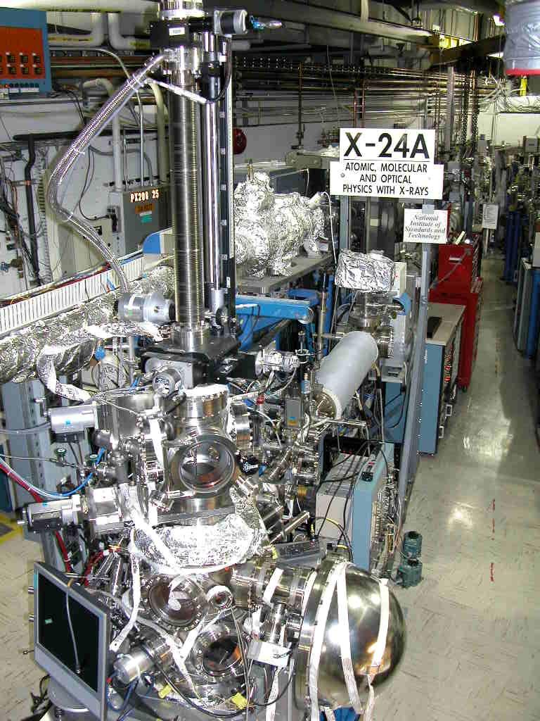
Hard X-ray Photoelectron Spectroscopy Research at NIST beamline X24A. Joseph C. Woicik NIST
|
|
|
- Valerie Grant
- 5 years ago
- Views:
Transcription
1 Hard X-ray Photoelectron Spectroscopy Research at NIST beamline X24A Joseph C. Woicik NIST
2 Outline Introduction to hard x-ray photoelectron spectroscopy (HAXPES) Semiconductor gate stacks on silicon Epitaxial, room temperature feroelectric SrTiO 3 on silicon Site Specific XPS and the nature of the solid state chemical bond: Cu, GaAs, TiO 2 N doping of TiO 2
 by tuning the X- ray excitation")


3 Hard X-ray Photoelectron Spectroscopy (HAXPES) Variable Kinetic Energy HAXPES Tune the HAXPES depth sensitivity (photoelectron kinetic energy) by tuning the X- ray excitation energy using a synchrotron X-ray beamline The U7A and X24A endstations form a unique measurement suite for surface to near bulk HAXPES by spanning X-ray excitation energy from 0.2 to 5 kev Example: Si electron binding energy 2p ~99 ev and 1s ~1840 ev, surface to bulk sensitivity (Lab source has fixed energy Al K Synchrotron Tool Photoelectron Kinetic Energy = h Binding Energy
4
5 Advantages of HAXPES
6 Advantages of HAXPES Study samples from air
7 Advantages of HAXPES Study samples from air; i.e., real samples!
8 Advantages of HAXPES Study samples from air; i.e., real samples! Tune λ for experimental system
9 Advantages of HAXPES Study samples from air; i.e., real samples! Tune λ for experimental system Variable kinetic energy XPS (VKE-XPS) for depth profiling
10 N o rm a liz e d In te n s ity (a rb. u n its ) P.S. Lysaght, J. Barnett, G.I. Bersuker, J.C. Woicik, D.A. Fischer, B. Foran, H.-H. Tseng, and R. Jammy Depth Sensitive VKE-XPS Si 1s h = 2100 ev h = 2500 ev h = 2600 ev HfO 2 SiO 2 h = 3000 ev 5 n m Si more oxidized less oxidized h = 3500 ev Si 2p "lab-like" spectrum h = 2100 ev Kinetic Energy (E-E c )
11 Advantages of HAXPES Study samples from air; i.e., real samples! Tune λ for experimental system Variable kinetic energy XPS (VKE-XPS) for depth profiling Bulk and surface sensitive core lines accessible for same element
12 Surface and Bulk Sensitive Core Lines Si 2p B.E. = 99 ev h = 2180 ev Si 1s B.E. = 1840 ev h = 2180 ev Kinetic Energy (ev) Kinetic Energy (ev)
13 Advantages of HAXPES Study samples from air; i.e., real samples! Tune λ for experimental system Variable kinetic energy XPS (VKE-XPS) for depth profiling Bulk and surface sensitive core lines accessible for same element Eliminate Auger interference
14 In te n s ity ( c o u n ts /s e c o n d ) Auger Interference Si KLL Auger O 1s Kinetic Energy (ev)
15 Advantages of HAXPES Study samples from air; i.e., real samples! Tune λ for experimental system Variable kinetic energy XPS (VKE-XPS) for depth profiling Bulk and surface sensitive core lines accessible for same element Eliminate Auger interference Photoemission and other techniques (SSXPS)
16 What is a gate stack? Metal SiO 2 Si
17 What is a gate stack? Metal SiO 2 Metal SiO 2 ~ 2 nm Si Si
18 What is a gate stack? Metal C = ε r ε o A/d ~ 2 nm HfO 2 K ~ 20 Metal ~ 1 nm SiO 2 K ~ 4 SiO 2 ~ 2 nm Si Si
 ) ) ) SEMATECH: HfO 2 /SiO 2 /Si Gate Stacks hv = 2200 ev NH 3 postdeposition anneal Hf 4f HfO 2 Hf-N HfO 2 SiO 2 A 5 n m Si NH 3 predeposition anneal HfO 2 N 1s hv = 2200 ev Hf-N B NH 3")
19 Intensity (a.u.) Intensity (a.u.) Intensity (a.u.) Intensity (a.u.) SEMATECH: HfO 2 /SiO 2 /Si Gate Stacks hv = 2200 ev NH 3 postdeposition anneal Hf 4f HfO 2 Hf-N HfO 2 SiO 2 A 5 n m Si NH 3 predeposition anneal HfO 2 N 1s hv = 2200 ev Hf-N B NH 3 postdeposition anneal A NH 3 pre- & postdeposition anneal HfO 2 Hf-N NH 3 predeposition anneal Si-N B Kinetic Energy (ev) C 2187 NH 3 pre- & post-deposition anneal Kinetic Energy (ev) P.S. Lysaght, J. Barnett, G.I. Bersuker, J.C. Woicik, D.A. Fischer, B. Foran, H.-H. Tseng, and R. Jammy C
 Motorola: 5 ML (20 Å) SrTiO 3 films on Si(001) Si 2p h = 2210 ev SiO 2")
20 In te n s ity (a rb. u n its ) Motorola: 5 ML (20 Å) SrTiO 3 films on Si(001) Si 2p h = 2210 ev SiO 2 /Si(001) SrTiO 3 /Si(001) Kinetic Energy (ev)
21 HfO 2 /SiGe/Si 2 nm HfO C anneal as deposited (300 C) 30 nm SiGe Si
22 In te n s ity (a rb. u n its ) In te n s ity (a rb. u n its ) SiGe h = 2140 ev Si 2p SiGe h = 2140 ev Si 1s Ge 3d Ge 2p Kinetic Energy (E - E c ) Kinetic Energy (E - E c )
23 In te n s ity (a rb. u n its ) Hf 4f as deposited h = 2140 ev 950 C anneal Kinetic Energy (ev)
24 In te n s ity (a rb. u n its ) Si 2p h = 2140 ev 950 C anneal as deposited SiGe Kinetic Energy (ev)
25 In te n s ity (a rb. u n its ) Si 1s h = 2140 ev 950 C anneal as deposited SiGe Kinetic Energy (ev)
26 In te n s ity ( a rb. u n its ) Ge 3d h = 2140 ev 950 C anneal as deposited SiGe Kinetic Energy (ev)
27 In te n s ity (a rb. u n its ) Ge 2p h = 2140 ev 950 C anneal as deposited SiGe Kinetic Energy (ev)
28 Advantages of HAXPES Study samples from air; i.e., real systems! Tune λ for experimental system Variable kinetic energy XPS (VKE-XPS) for depth profiling Bulk and surface sensitive core lines accessible for same element Eliminate Auger interference Photoemission and other techniques (SSXPS)
29 Electronic Structure of GaAs J. Chelikowsky, D.J. Chadi, and M.L. Cohen
30 X-ray Standing Waves Bragg's Law: H H = k h - k o k o k h Electric Field: ^. ^. E(r,t) = [ E o e ik o r + E h e ik h r ] e -i t Electric Field Intensity:. I(r) = E E* = E o 2 [ 1 + R + 2 R cos( + H. r ) ] where E h / E o = R e i and 0 < <
31 Bragg Diffraction: = 2d sin( ) d R Reflectivity E B XSW Yield Y E B
32 In te n s i ty (a rb. u n i ts ) Ga As d 111
33 In te n s ity (c n ts./s e c o n d ) 200 As 3d GaAs Ga 3d Valence Band Kinetic Energy (ev) (E - E ) VBM
34 In te n s ity (a rb itra ry u n its ) V a le n c e B a n d T h e o ry E x p e rim e n t G a A s K in e tic E n e rg y (E - E ) V B M

35 Electronic Structure of Cu J. Friis, B. Jiang, K. Marthinsen, and R. Holmestad
36 In te n s ity (a rb. u n its ) Cu(11-1) Cu (valence) Cu 3p (core) Photon Energy (ev)
37 In te n s ity (a rb. u n its ) Cu(11-1) valence spectra Kinetic Energy (ev)
38 N o rm a liz e d In te n s ity (a rb. u n its ) Cu(11-1) valence spectra What happened to the free-electron theory of metals? Kinetic Energy (ev) (E - E f )
39 E.L. Shirley Photoemission process Feynman diagram: hole What is left behind. photoelectron What comes out of the crystal. photon What goes in the crystal. Electron/hole propagators are shown by solid lines. This process is forbidden for free electrons because of energy/momentum conservation.
40 E.L. Shirley Photoemission process Feynman diagram: hole What is left behind. photon What goes in the crystal. photoelectron What comes out of the crystal. Phonon lattice recoil Electron/hole propagators are shown by solid lines. This process is forbidden for free electrons because of energy/momentum conservation.
41 Recoil Effects of Photoelectrons in a Solid Y. Takata, Y. Kayanuma, M. Yabashi, K. Tamasaku, Y. Nishino, D. Miwa, Y. Harada, K. Horiba, S. Shin, S. Tanaka, E. Ikenaga, K. Kobayashi, Y. Senba, H. Ohashi, and T. Ishikawa
42 In te n s ity (a rb. u n its ) Electronic Structure of Rutile TiO 2 DOS theory expt. c-theory Energy (ev) (E - E ) VBM

43 O T i b c a
44 In te n s ity (a rb. u n its ) Ti 3p TiO (110) 2 O 2s VB Energy (ev) (E - E ) VBM
45 In te n s ity (a rb. u n its ) (a) DOS theory expt. (b) pdos Ti expt. O x 4 expt Energy (ev) (E - E ) VBM
46 Chemical Hybridization
47 In te n s ity (a rb. u n its ) (a) DOS theory expt. (b) pdos Ti σ π expt. O O-π x 4 expt Energy (ev) (E - E ) VBM
48 In te n s ity (a rb. u n its ) (a) pdos Ti theory expt. (b) pdos O theory expt Energy (ev) (E - E ) VBM
49 In te n s ity (a rb. u n its ) lpdos O 2p x 1.0 O 2s x 110 Ti 3d x 1.8 Ti 4p x 11 Ti 4s x Energy (ev) (E - E ) VBM
50 Theoretical Atomic Cross Sections σti 4s 30! σ Ti 3d σo 2s 10! σ O 2p XPS favors states with smaller values of angular momentum! I(E,ħω) α i,l ρ i,l (E) σ i,l (E,ħω)
51 In te n s ity (a rb. u n its ) (a) pdos Ti c-theory expt. (b) pdos O c-theory expt Energy (ev) (E - E ) VBM
52 In te n s ity (a rb. u n its ) Electronic Structure of Rutile TiO 2 DOS theory expt. c-theory Energy (ev) (E - E ) VBM
53 In te n s ity (a rb. u n its ) Ti 3p TiO (110) 2 O 2s VB Energy (ev) (E - E ) VBM
54 N doped TiO 2 (anatase) Ti 2p
55
56 lpdos
57 Electronic Structure of TiO 2 (anatase)
58 lpdos
59 Electronic Structure of N doped TiO 2 (anatase)
60 Many Thanks Daniel Fischer (NIST) and Barry Karlin (NIST) Pat Lysaght (SEMATECH) Hao Li (Motorola Labs) Erik Nelson (SSRL), David Heskett (URI), and Lonny Berman (NSLS) Leeor Kronik (Weizmann) and Jim Chelikowsky (Austin) Abdul Rumaiz (NSLS) and Eric Cockayne (NIST)

61
62 In te n s ity (c n ts./s e c ) 3 0 G a 2 0 A s 1 0 to ta l K in e tic E n e rg y (E - E V B M ) e V
63 d d ik. < f e ( o r. p ) i > 2 H o = i p i 2 /2m + V( r ) H ' = A o. p E kin = h - E b (h >> E b ) f > = e ik f. r (k f >> k o ) [p,h] = -i h V( r ) d d < f. V( r ) i > 2
64 V a le n c e P h o to e m is s io n f > i > V ( r ) d d ik. o r ^. < f e ( p ) i > 2
65 Chemical Hybridization = - + 2p z λ2s λ2s + 2p z 2p λ2s - 2p z 2s λ2s + 2p z s-p hybrid H i,j = ψ i H ψ j dv Stronger Chemical Bond!
J. Price, 1,2 Y. Q. An, 1 M. C. Downer 1 1 The university of Texas at Austin, Department of Physics, Austin, TX
 Understanding process-dependent oxygen vacancies in thin HfO 2 /SiO 2 stacked-films on Si (100) via competing electron-hole injection dynamic contributions to second harmonic generation. J. Price, 1,2
Introduction to X-ray Photoelectron Spectroscopy (XPS) XPS which makes use of the photoelectric effect, was developed in the mid-1960
 XPS which makes use of the photoelectric effect, was developed in the mid-1960") Introduction to X-ray Photoelectron Spectroscopy (XPS) X-ray Photoelectron Spectroscopy (XPS), also known as Electron Spectroscopy for Chemical Analysis (ESCA) is a widely used technique to investigate
Introduction to X-ray Photoelectron Spectroscopy (XPS) X-ray Photoelectron Spectroscopy (XPS), also known as Electron Spectroscopy for Chemical Analysis (ESCA) is a widely used technique to investigate
Photon Interaction. Spectroscopy
 Photon Interaction Incident photon interacts with electrons Core and Valence Cross Sections Photon is Adsorbed Elastic Scattered Inelastic Scattered Electron is Emitted Excitated Dexcitated Stöhr, NEXAPS
Probing Matter: Diffraction, Spectroscopy and Photoemission
 Probing Matter: Diffraction, Spectroscopy and Photoemission Anders Nilsson Stanford Synchrotron Radiation Laboratory Why X-rays? VUV? What can we hope to learn? 1 Photon Interaction Incident photon interacts
Energy Spectroscopy. Excitation by means of a probe
 Energy Spectroscopy Excitation by means of a probe Energy spectral analysis of the in coming particles -> XAS or Energy spectral analysis of the out coming particles Different probes are possible: Auger
Energy Spectroscopy. Ex.: Fe/MgO
 Energy Spectroscopy Spectroscopy gives access to the electronic properties (and thus chemistry, magnetism,..) of the investigated system with thickness dependence Ex.: Fe/MgO Fe O Mg Control of the oxidation
Resonant photo-ionization of point defects in HfO 2 thin films observed by second-harmonic generation.
 Optics of Surfaces & Interfaces - VIII September 10 th, 2009 Resonant photo-ionization of point defects in HfO 2 thin films observed by second-harmonic generation. Jimmy Price and Michael C. Downer Physics
Studying Metal to Insulator Transitions in Solids using Synchrotron Radiation-based Spectroscopies.
 PY482 Lecture. February 28 th, 2013 Studying Metal to Insulator Transitions in Solids using Synchrotron Radiation-based Spectroscopies. Kevin E. Smith Department of Physics Department of Chemistry Division
X-ray Photoelectron Spectroscopy (XPS)
") X-ray Photoelectron Spectroscopy (XPS) As part of the course Characterization of Catalysts and Surfaces Prof. Dr. Markus Ammann Paul Scherrer Institut markus.ammann@psi.ch Resource for further reading:
X-ray Photoelectron Spectroscopy (XPS) As part of the course Characterization of Catalysts and Surfaces Prof. Dr. Markus Ammann Paul Scherrer Institut markus.ammann@psi.ch Resource for further reading:
X-ray Spectroscopy Theory Lectures
 TIMES Lecture Series SIMES-SLAC-Stanford Winter, 2017 X-ray Spectroscopy Theory Lectures J. J. Rehr I. Introduction to the Theory of X-ray spectra II. Real-space Green's function Theory and FEFF III. Inelastic
X-Ray Standing-Wave Investigations of Valence Electronic Structure
 University of Rhode Island DigitalCommons@URI Physics Faculty Publications Physics 2001 X-Ray Standing-Wave Investigations of Valence Electronic Structure J. C. Woicik E. J. Nelson See next page for additional
Spectroscopy of Nanostructures. Angle-resolved Photoemission (ARPES, UPS)
") Spectroscopy of Nanostructures Angle-resolved Photoemission (ARPES, UPS) Measures all quantum numbers of an electron in a solid. E, k x,y, z, point group, spin E kin, ϑ,ϕ, hν, polarization, spin Electron
Spectroscopy of Nanostructures Angle-resolved Photoemission (ARPES, UPS) Measures all quantum numbers of an electron in a solid. E, k x,y, z, point group, spin E kin, ϑ,ϕ, hν, polarization, spin Electron
X-ray Absorption at the Near-edge and Its Applications
 X-ray Absorption at the Near-edge and Its Applications Faisal M Alamgir faisal@msegatechedu School of Materials Science and Engineering, Georgia Institute of Technology Cartoon of XAS ln(i 0 /I t ) or
Lecture 7 Chemical/Electronic Structure of Glass
 Lecture 7 Chemical/Electronic Structure of Glass Syllabus Topic 6. Electronic spectroscopy studies of glass structure Fundamentals and Applications of X-ray Photoelectron Spectroscopy (XPS) a.k.a. Electron
Core Level Spectroscopies
 Core Level Spectroscopies Spectroscopies involving core levels are element-sensitive, and that makes them very useful for understanding chemical bonding, as well as for the study of complex materials.
Direct and Indirect Semiconductor
 Direct and Indirect Semiconductor Allowed values of energy can be plotted vs. the propagation constant, k. Since the periodicity of most lattices is different in various direction, the E-k diagram must
development of the hard-x-ray angle Resolved X-ray Photoemission spectrometer for Laboratory use
 ANALYTICAL SCIENCES FEBRUARY 2010, VOL. 26 227 2010 The Japan Society for Analytical Chemistry development of the hard-x-ray angle Resolved X-ray Photoemission spectrometer for Laboratory use masaaki kobata,*
Angle-Resolved Two-Photon Photoemission of Mott Insulator
 Angle-Resolved Two-Photon Photoemission of Mott Insulator Takami Tohyama Institute for Materials Research (IMR) Tohoku University, Sendai Collaborators IMR: H. Onodera, K. Tsutsui, S. Maekawa H. Onodera
Two-dimensional lattice
 Two-dimensional lattice a 1 *, k x k x =0,k y =0 X M a 2, y Γ X a 2 *, k y a 1, x Reciprocal lattice Γ k x = 0.5 a 1 *, k y =0 k x = 0, k y = 0.5 a 2 * k x =0.5a 1 *, k y =0.5a 2 * X X M k x = 0.25 a 1
Name: (a) What core levels are responsible for the three photoelectron peaks in Fig. 1?
 What core levels are responsible for the three photoelectron peaks in Fig. 1?") Physics 243A--Surface Physics of Materials: Spectroscopy Final Examination December 16, 2014 (3 problems, 100 points total, open book, open notes and handouts) Name: [1] (50 points), including Figures
Physics 243A--Surface Physics of Materials: Spectroscopy Final Examination December 16, 2014 (3 problems, 100 points total, open book, open notes and handouts) Name: [1] (50 points), including Figures
Crystal Properties. MS415 Lec. 2. High performance, high current. ZnO. GaN
 Crystal Properties Crystal Lattices: Periodic arrangement of atoms Repeated unit cells (solid-state) Stuffing atoms into unit cells Determine mechanical & electrical properties High performance, high current
Study of semiconductors with positrons. Outlook:
 Study of semiconductors with positrons V. Bondarenko, R. Krause-Rehberg Martin-Luther-University Halle-Wittenberg, Halle, Germany Introduction Positron trapping into defects Methods of positron annihilation
MS482 Materials Characterization ( 재료분석 ) Lecture Note 5: RBS
 Lecture Note 5: RBS") 2016 Fall Semester MS482 Materials Characterization ( 재료분석 ) Lecture Note 5: RBS Byungha Shin Dept. of MSE, KAIST 1 Course Information Syllabus 1. Overview of various characterization techniques (1 lecture)
2016 Fall Semester MS482 Materials Characterization ( 재료분석 ) Lecture Note 5: RBS Byungha Shin Dept. of MSE, KAIST 1 Course Information Syllabus 1. Overview of various characterization techniques (1 lecture)
Electron Microscopy I
 Characterization of Catalysts and Surfaces Characterization Techniques in Heterogeneous Catalysis Electron Microscopy I Introduction Properties of electrons Electron-matter interactions and their applications
IV. Surface analysis for chemical state, chemical composition
 IV. Surface analysis for chemical state, chemical composition Probe beam Detect XPS Photon (X-ray) Photoelectron(core level electron) UPS Photon (UV) Photoelectron(valence level electron) AES electron
XPS Study of Ultrathin GeO 2 /Ge System
 XPS Study of Ultrathin GeO 2 /Ge System Akio Ohta, Hiroaki Furukawa, Hiroshi Nakagawa, Hideki Murakami, Seiichirou Higashi and Seiichi Miyazaki Graduate School of Adavanced Sciences of Matter, Hiroshima
Inelastic soft x-ray scattering, fluorescence and elastic radiation
 Inelastic soft x-ray scattering, fluorescence and elastic radiation What happens to the emission (or fluorescence) when the energy of the exciting photons changes? The emission spectra (can) change. One
Site-specific electron diffraction resolved via nuclear recoil
 Site-specific electron diffraction resolved via nuclear recoil Aimo Winkelmann Maarten Vos Max-Planck-Institut für Mikrostrukturphysik Halle (Saale), Germany Research School of Physics and Engineering
Development of hard X-ray photoelectron spectroscopy at BL29XU in SPring-8
 Nuclear Instruments and Methods in Physics Research A 547 (2005) 50 55 www.elsevier.com/locate/nima Development of hard X-ray photoelectron spectroscopy at BL29XU in SPring-8 Y. Takata a,, M. Yabashi b,c,
Brookhaven National Laboratory ABSTRACT
 10.1149/1.2209280, copyright The Electrochemical Society THE INFLUENCE OF NH 3 ANNEAL ON THE CRYSTALLIZATION KINETICS OF HfO 2 GATE DIELECTRIC FILMS Patrick S. Lysaght 1), J. C. Woicik 2), Brendan Foran
Electron Spettroscopies
 Electron Spettroscopies Spettroscopy allows to characterize a material from the point of view of: chemical composition, electronic states and magnetism, electronic, roto-vibrational and magnetic excitations.
The design of an integrated XPS/Raman spectroscopy instrument for co-incident analysis
 The design of an integrated XPS/Raman spectroscopy instrument for co-incident analysis Tim Nunney The world leader in serving science 2 XPS Surface Analysis XPS +... UV Photoelectron Spectroscopy UPS He(I)
Electron Rutherford Backscattering, a versatile tool for the study of thin films
 Electron Rutherford Backscattering, a versatile tool for the study of thin films Maarten Vos Research School of Physics and Engineering Australian National University Canberra Australia Acknowledgements:
Photoelectron Peak Intensities in Solids
 Photoelectron Peak Intensities in Solids Electronic structure of solids Photoelectron emission through solid Inelastic scattering Other excitations Intrinsic and extrinsic Shake-up, shake-down and shake-off
Surface and Electronic Structure Study of Substrate-dependent Pyrite Thin Films
 Surface and Electronic Structure Study of Substrate-dependent Pyrite Thin Films Talk Outline Stoichiometry and sodium study of pyrite thin films: Quick Review Surface structure of pyrite thin films Electronic
Supporting information Chemical Design and Example of Transparent Bipolar Semiconductors
 Supporting information Chemical Design and Example of Transparent Bipolar Semiconductors Takeshi Arai 1, Soshi Iimura 1, *, Junghwan Kim 2, Yoshitake Toda 2, Shigenori Ueda 3, 4, and Hideo Hosono 1, 2,
Lecture 23 X-Ray & UV Techniques
 Lecture 23 X-Ray & UV Techniques Schroder: Chapter 11.3 1/50 Announcements Homework 6/6: Will be online on later today. Due Wednesday June 6th at 10:00am. I will return it at the final exam (14 th June).
ELEMENTARY BAND THEORY
 ELEMENTARY BAND THEORY PHYSICIST Solid state band Valence band, VB Conduction band, CB Fermi energy, E F Bloch orbital, delocalized n-doping p-doping Band gap, E g Direct band gap Indirect band gap Phonon
MS482 Materials Characterization ( 재료분석 ) Lecture Note 4: XRF
 Lecture Note 4: XRF") 2016 Fall Semester MS482 Materials Characterization ( 재료분석 ) Lecture Note 4: XRF Byungha Shin Dept. of MSE, KAIST 1 Course Information Syllabus 1. Overview of various characterization techniques (1 lecture)
2016 Fall Semester MS482 Materials Characterization ( 재료분석 ) Lecture Note 4: XRF Byungha Shin Dept. of MSE, KAIST 1 Course Information Syllabus 1. Overview of various characterization techniques (1 lecture)
Surface Characte i r i zat on LEED Photoemission Phot Linear optics
 Surface Characterization i LEED Photoemission Linear optics Surface characterization with electrons MPS M.P. Seah, WA W.A. Dench, Surf. Interf. Anal. 1 (1979) 2 LEED low energy electron diffraction De
Sponsored by. Contract No. N K-0073: Modification P00006 DARPA Order 5674 NR
 OTIC FILE COP Study of Interfacial Chemistry between Metals and Their Effects on Electronic Systems q. o Sponsored by 00 Defense Advanced Research Projects Agency (DOD) and The Office of Naval Research
X-ray Standing-Wave Investigation of (1X2)Rb/ Cu(110)
Rb/ Cu(110)") University of Rhode Island DigitalCommons@URI Physics Faculty Publications Physics 2000 X-ray Standing-Wave Investigation of (1X2)Rb/ Cu(110) David R. Heskett University of Rhode Island, dheskett@uri.edu
University of Rhode Island DigitalCommons@URI Physics Faculty Publications Physics 2000 X-ray Standing-Wave Investigation of (1X2)Rb/ Cu(110) David R. Heskett University of Rhode Island, dheskett@uri.edu
MS482 Materials Characterization ( 재료분석 ) Lecture Note 2: UPS
 Lecture Note 2: UPS") 2016 Fall Semester MS482 Materials Characterization ( 재료분석 ) Lecture Note 2: UPS Byungha Shin Dept. of MSE, KAIST 1 Course Information Syllabus 1. Overview of various characterization techniques (1 lecture)
2016 Fall Semester MS482 Materials Characterization ( 재료분석 ) Lecture Note 2: UPS Byungha Shin Dept. of MSE, KAIST 1 Course Information Syllabus 1. Overview of various characterization techniques (1 lecture)
X-Ray Photoelectron Spectroscopy (XPS)-2
-2") X-Ray Photoelectron Spectroscopy (XPS)-2 Louis Scudiero http://www.wsu.edu/~scudiero; 5-2669 Fulmer 261A Electron Spectroscopy for Chemical Analysis (ESCA) The 3 step model: 1.Optical excitation 2.Transport
X-Ray Photoelectron Spectroscopy (XPS)-2 Louis Scudiero http://www.wsu.edu/~scudiero; 5-2669 Fulmer 261A Electron Spectroscopy for Chemical Analysis (ESCA) The 3 step model: 1.Optical excitation 2.Transport
SUPPLEMENTARY INFORMATION
 SUPPLEMENTARY INFORMATION Conductance Measurements The conductance measurements were performed at the University of Aarhus. The Ag/Si surface was prepared using well-established procedures [1, 2]. After
REPORT DOCUMENTATION PAGE
 REPORT DOCUMENTATION PAGE Form Approved OMB NO. 0704-0188 Public Reporting burden for this collection of information is estimated to average 1 hour per response, including the time for reviewing instructions,
Chemistry Instrumental Analysis Lecture 8. Chem 4631
 Chemistry 4631 Instrumental Analysis Lecture 8 UV to IR Components of Optical Basic components of spectroscopic instruments: stable source of radiant energy transparent container to hold sample device
4. How can fragmentation be useful in identifying compounds? Permits identification of branching not observed in soft ionization.
 Homework 9: Chapters 20-21 Assigned 12 April; Due 17 April 2006; Quiz on 19 April 2006 Chap. 20 (Molecular Mass Spectroscopy) Chap. 21 (Surface Analysis) 1. What are the types of ion sources in molecular
X-ray Spectroscopy. Interaction of X-rays with matter XANES and EXAFS XANES analysis Pre-edge analysis EXAFS analysis
 X-ray Spectroscopy Interaction of X-rays with matter XANES and EXAFS XANES analysis Pre-edge analysis EXAFS analysis Element specific Sensitive to low concentrations (0.01-0.1 %) Why XAS? Applicable under
SEMICONDUCTOR PHYSICS
 SEMICONDUCTOR PHYSICS by Dibyendu Chowdhury Semiconductors The materials whose electrical conductivity lies between those of conductors and insulators, are known as semiconductors. Silicon Germanium Cadmium
ENERGY BANDS AND GAPS IN SEMICONDUCTOR. Muhammad Hafeez Javed
 ENERGY BANDS AND GAPS IN SEMICONDUCTOR Muhammad Hafeez Javed www.rmhjaved.com rmhjaved@gmail.com Out Line Introduction Energy band Classification of materials Direct and indirect band gap of SC Classification
Shu Hu 1,2, Matthias H. Richter 1,2, Michael F. Lichterman 1,2, Joseph Beardslee 2,4, Thomas Mayer 5, Bruce S. Brunschwig 1 and Nathan S.
 Supporting Information for: Electrical, Photoelectrochemical and Photoelectron Spectroscopic Investigation of the Interfacial Transport and Energetics of Amorphous TiO 2 /Si Heterojunctions Shu Hu 1,2,
Birck Nanotechnology Center XPS: X-ray Photoelectron Spectroscopy ESCA: Electron Spectrometer for Chemical Analysis
 Birck Nanotechnology Center XPS: X-ray Photoelectron Spectroscopy ESCA: Electron Spectrometer for Chemical Analysis Dmitry Zemlyanov Birck Nanotechnology Center, Purdue University Outline Introduction
single-layer transition metal dichalcogenides MC2
 single-layer transition metal dichalcogenides MC2 Period 1 1 H 18 He 2 Group 1 2 Li Be Group 13 14 15 16 17 18 B C N O F Ne 3 4 Na K Mg Ca Group 3 4 5 6 7 8 9 10 11 12 Sc Ti V Cr Mn Fe Co Ni Cu Zn Al Ga
X-Ray Photoelectron Spectroscopy (XPS)
") X-Ray Photoelectron Spectroscopy (XPS) Louis Scudiero http://www.wsu.edu/~scudiero; 5-2669 Fulmer 261A Electron Spectroscopy for Chemical Analysis (ESCA) The basic principle of the photoelectric effect
X-Ray Photoelectron Spectroscopy (XPS) Louis Scudiero http://www.wsu.edu/~scudiero; 5-2669 Fulmer 261A Electron Spectroscopy for Chemical Analysis (ESCA) The basic principle of the photoelectric effect
MS482 Materials Characterization ( 재료분석 ) Lecture Note 5: RBS. Byungha Shin Dept. of MSE, KAIST
 Lecture Note 5: RBS. Byungha Shin Dept. of MSE, KAIST") 2015 Fall Semester MS482 Materials Characterization ( 재료분석 ) Lecture Note 5: RBS Byungha Shin Dept. of MSE, KAIST 1 Course Information Syllabus 1. Overview of various characterization techniques (1 lecture)
2015 Fall Semester MS482 Materials Characterization ( 재료분석 ) Lecture Note 5: RBS Byungha Shin Dept. of MSE, KAIST 1 Course Information Syllabus 1. Overview of various characterization techniques (1 lecture)
Two-dimensional lattice
 1 Two-dimensional lattice a 1 *, k x k x = 0, k y = 0 X M a 2, y a 1, x Γ X a 2 *, k y k x = 0.5 a 1 *, k y = 0 k x = 0, k y = 0.5 a 2 * Γ k x = 0.5 a 1 *, k y = 0.5 a 2 * X X M k x = 0.25 a 1 *, k y =
X-Ray Photoelectron Spectroscopy (XPS)-2
-2") X-Ray Photoelectron Spectroscopy (XPS)-2 Louis Scudiero http://www.wsu.edu/~pchemlab ; 5-2669 Fulmer 261A Electron Spectroscopy for Chemical Analysis (ESCA) The 3 step model: 1.Optical excitation 2.Transport
X-Ray Photoelectron Spectroscopy (XPS)-2 Louis Scudiero http://www.wsu.edu/~pchemlab ; 5-2669 Fulmer 261A Electron Spectroscopy for Chemical Analysis (ESCA) The 3 step model: 1.Optical excitation 2.Transport
Advanced Lab Course. X-Ray Photoelectron Spectroscopy 1 INTRODUCTION 1 2 BASICS 1 3 EXPERIMENT Qualitative analysis Chemical Shifts 7
 Advanced Lab Course X-Ray Photoelectron Spectroscopy M210 As of: 2015-04-01 Aim: Chemical analysis of surfaces. Content 1 INTRODUCTION 1 2 BASICS 1 3 EXPERIMENT 3 3.1 Qualitative analysis 6 3.2 Chemical
The Use of Synchrotron Radiation in Modern Research
 The Use of Synchrotron Radiation in Modern Research Physics Chemistry Structural Biology Materials Science Geochemical and Environmental Science Atoms, molecules, liquids, solids. Electronic and geometric
5) Surface photoelectron spectroscopy. For MChem, Spring, Dr. Qiao Chen (room 3R506) University of Sussex.
 Surface photoelectron spectroscopy. For MChem, Spring, Dr. Qiao Chen (room 3R506) University of Sussex.") For MChem, Spring, 2009 5) Surface photoelectron spectroscopy Dr. Qiao Chen (room 3R506) http://www.sussex.ac.uk/users/qc25/ University of Sussex Today s topics 1. Element analysis with XPS Binding energy,
For MChem, Spring, 2009 5) Surface photoelectron spectroscopy Dr. Qiao Chen (room 3R506) http://www.sussex.ac.uk/users/qc25/ University of Sussex Today s topics 1. Element analysis with XPS Binding energy,
Angle-resolved photoemission spectroscopy (ARPES) Overview-Physics 250, UC Davis Inna Vishik
 Overview-Physics 250, UC Davis Inna Vishik") Angle-resolved photoemission spectroscopy (ARPES) Overview-Physics 250, UC Davis Inna Vishik Outline Review: momentum space and why we want to go there Looking at data: simple metal Formalism: 3 step model
Angle-resolved photoemission spectroscopy (ARPES) Overview-Physics 250, UC Davis Inna Vishik Outline Review: momentum space and why we want to go there Looking at data: simple metal Formalism: 3 step model
X-Ray Photoelectron Spectroscopy (XPS)
") X-Ray Photoelectron Spectroscopy (XPS) Louis Scudiero http://www.wsu.edu/~scudiero; 5-2669 Electron Spectroscopy for Chemical Analysis (ESCA) The basic principle of the photoelectric effect was enunciated
X-Ray Photoelectron Spectroscopy (XPS) Louis Scudiero http://www.wsu.edu/~scudiero; 5-2669 Electron Spectroscopy for Chemical Analysis (ESCA) The basic principle of the photoelectric effect was enunciated
Photoelectron Interference Pattern (PEIP): A Two-particle Bragg-reflection Demonstration
: A Two-particle Bragg-reflection Demonstration") Photoelectron Interference Pattern (PEIP): A Two-particle Bragg-reflection Demonstration Application No. : 2990 Beamlime: BL25SU Project Leader: Martin Månsson 0017349 Team Members: Dr. Oscar Tjernberg
Photoelectron Interference Pattern (PEIP): A Two-particle Bragg-reflection Demonstration Application No. : 2990 Beamlime: BL25SU Project Leader: Martin Månsson 0017349 Team Members: Dr. Oscar Tjernberg
Making the Invisible Visible: Probing Antiferromagnetic Order in Novel Materials
 Making the Invisible Visible: Probing Antiferromagnetic Order in Novel Materials Elke Arenholz Lawrence Berkeley National Laboratory Antiferromagnetic contrast in X-ray absorption Ni in NiO Neel Temperature
Electronic structure of transition metal high-k dielectrics: interfacial band offset energies for microelectronic devices
 Applied Surface Science 212 213 (2003) 563 569 Electronic structure of transition metal high-k dielectrics: interfacial band offset energies for microelectronic devices Gerald Lucovsky *, Gilbert B. Rayner
Introduction to Semiconductor Physics. Prof.P. Ravindran, Department of Physics, Central University of Tamil Nadu, India
 Introduction to Semiconductor Physics 1 Prof.P. Ravindran, Department of Physics, Central University of Tamil Nadu, India http://folk.uio.no/ravi/cmp2013 Review of Semiconductor Physics Semiconductor fundamentals
Atomic Physics. Chapter 6 X ray. Jinniu Hu 24/12/ /20/13
 Atomic Physics Chapter 6 X ray 11/20/13 24/12/2018 Jinniu Hu 1!1 6.1 The discovery of X ray X-rays were discovered in 1895 by the German physicist Wilhelm Roentgen. He found that a beam of high-speed electrons
structure and paramagnetic character R. Kakavandi, S-A. Savu, A. Caneschi, T. Chassé, M. B. Casu Electronic Supporting Information
 At the interface between organic radicals and TiO 2 (110) single crystals: electronic structure and paramagnetic character R. Kakavandi, S-A. Savu, A. Caneschi, T. Chassé, M. B. Casu Electronic Supporting
Lecture 12 Multiplet splitting
 Lecture 12 Multiplet splitting Multiplet splitting Atomic various L and S terms Both valence and core levels Rare earths Transition metals Paramagnetic free molecules Consider 3s level emission from Mn2+
In-situ photoemission study of La 1 x Sr x FeO 3 epitaxial thin films
 In-situ photoemission study of La 1 x Sr x FeO 3 epitaxial thin films Master Thesis Hiroki Wadati Department of Physics, University of Tokyo January, 2004 Contents 1 Introduction 1 2 Principles of photoemission
Surface Electron Spectroscopies: Principles and Applications
 Surface Electron Spectroscopies: Principles and Applications S. Kaciulis, A. Mezzi CNR - Istituto per lo Studio dei Materiali Nanostrutturati, Area della Ricerca Roma 1 Area della Ricerca di Roma 1 Via
MSE 321 Structural Characterization
 Auger Spectroscopy Auger Electron Spectroscopy (AES) Scanning Auger Microscopy (SAM) Incident Electron Ejected Electron Auger Electron Initial State Intermediate State Final State Physical Electronics
Methods of surface analysis
 Methods of surface analysis Nanomaterials characterisation I RNDr. Věra Vodičková, PhD. Surface of solid matter: last monoatomic layer + absorbed monolayer physical properties are effected (crystal lattice
Solid State Device Fundamentals
 Solid State Device Fundamentals ENS 345 Lecture Course by Alexander M. Zaitsev alexander.zaitsev@csi.cuny.edu Tel: 718 982 2812 Office 4N101b 1 The free electron model of metals The free electron model
Soft X-ray Physics DELNOR-WIGGINS PASS STATE PARK
 Soft X-ray Physics Overview of research in Prof. Tonner s group Introduction to synchrotron radiation physics Photoemission spectroscopy: band-mapping and photoelectron diffraction Magnetic spectroscopy
Introduction to Engineering Materials ENGR2000. Dr.Coates
 Introduction to Engineering Materials ENGR2000 Chapter 18: Electrical Properties Dr.Coates 18.2 Ohm s Law V = IR where R is the resistance of the material, V is the voltage and I is the current. l R A
Auger Electron Spectroscopy
 Auger Electron Spectroscopy Auger Electron Spectroscopy is an analytical technique that provides compositional information on the top few monolayers of material. Detect all elements above He Detection
The photoelectric effect
 The photoelectric effect E K hν-e B E F hν E B A photoemission experiment Lifetime broadening ΔE.Δτ~ħ ΔE~ħ/Δτ + Experimental resolution Hüfner, Photoelectron Spectroscopy (Springer) A photoemission experiment
Atomic Layer Deposition of Hafnium Oxide at Temperatures below 100ºC. K. C. Kragh
 Atomic Layer Deposition of Hafnium Oxide at Temperatures below 100ºC K. C. Kragh Dept. of Physics and Optical Engineering, Rose-Hulman Institute of Technology REU Student in the Advanced Materials Research
Lecture 17 Auger Electron Spectroscopy
 Lecture 17 Auger Electron Spectroscopy Auger history cloud chamber Although Auger emission is intense, it was not used until 1950 s. Evolution of vacuum technology and the application of Auger Spectroscopy
The electronic structure of solids. Charge transport in solids
 The electronic structure of solids We need a picture of the electronic structure of solid that we can use to explain experimental observations and make predictions Why is diamond an insulator? Why is sodium
Intensity / a.u. 2 theta / deg. MAPbI 3. 1:1 MaPbI 3-x. Cl x 3:1. Supplementary figures
 Intensity / a.u. Supplementary figures 110 MAPbI 3 1:1 MaPbI 3-x Cl x 3:1 220 330 0 10 15 20 25 30 35 40 45 2 theta / deg Supplementary Fig. 1 X-ray Diffraction (XRD) patterns of MAPbI3 and MAPbI 3-x Cl
Spectroscopy at nanometer scale
 Spectroscopy at nanometer scale 1. Physics of the spectroscopies 2. Spectroscopies for the bulk materials 3. Experimental setups for the spectroscopies 4. Physics and Chemistry of nanomaterials Various
Auger Electron Spectroscopy (AES)
") 1. Introduction Auger Electron Spectroscopy (AES) Silvia Natividad, Gabriel Gonzalez and Arena Holguin Auger Electron Spectroscopy (Auger spectroscopy or AES) was developed in the late 1960's, deriving
1. Introduction Auger Electron Spectroscopy (AES) Silvia Natividad, Gabriel Gonzalez and Arena Holguin Auger Electron Spectroscopy (Auger spectroscopy or AES) was developed in the late 1960's, deriving
Electron Spectroscopy
 Electron Spectroscopy Photoelectron spectroscopy is based upon a single photon in/electron out process. The energy of a photon is given by the Einstein relation : E = h ν where h - Planck constant ( 6.62
Nearly Free Electron Gas model - II
 Nearly Free Electron Gas model - II Contents 1 Lattice scattering 1 1.1 Bloch waves............................ 2 1.2 Band gap formation........................ 3 1.3 Electron group velocity and effective
ESE 372 / Spring 2013 / Lecture 5 Metal Oxide Semiconductor Field Effect Transistor
 Metal Oxide Semiconductor Field Effect Transistor V G V G 1 Metal Oxide Semiconductor Field Effect Transistor We will need to understand how this current flows through Si What is electric current? 2 Back
Chapter 1 Hard X-ray Photoemission: An Overview and Future Perspective
 Chapter 1 Hard X-ray Photoemission: An Overview and Future Perspective Charles S. Fadley Abstract The various aspects of hard X-ray photoemission are reviewed, including in particular more newly developed
Photoemission Spectroscopy: Fundamental Aspects
 Photoemission Spectroscopy: Fundamental Aspects G. Stefani Dipartimento di Scienze,Universita Roma Tre CNISM Unita di Ricerca di Roma 3 XIV SILS School G. Stefani 1 hn Basic Concepts - E e E, e K e ˆ E
Department of Electrical Engineering and Information Systems, Tanaka-Ohya lab.
 Observation of the room-temperature local ferromagnetism and its nanoscale expansion in the ferromagnetic semiconductor Ge 1 xfe x Yuki K. Wakabayashi 1 and Yukio Takahashi 2 1 Department of Electrical
ET3034TUx Utilization of band gap energy
 ET3034TUx - 3.3.1 - Utilization of band gap energy In the last two weeks we have discussed the working principle of a solar cell and the external parameters that define the performance of a solar cell.
Solid State Device Fundamentals
 Solid State Device Fundamentals ENS 345 Lecture Course by Alexander M. Zaitsev alexander.zaitsev@csi.cuny.edu Tel: 718 982 2812 Office 4N101b 1 Outline - Goals of the course. What is electronic device?
The effectiveness of HCl and HF cleaning of Si 0.85 Ge 0.15 surface. Stanford Synchrotron Radiation Lab, Menlo Park, CA 94025
 July 2008 SLAC-PUB-13302 The effectiveness of HCl and HF cleaning of Si 0.85 Ge 0.15 surface Yun Sun, a) Zhi Liu, Shiyu Sun, Piero Pianetta Stanford Synchrotron Radiation Lab, Menlo Park, CA 94025 The
ATOMIC-SCALE THEORY OF RADIATION-INDUCED PHENOMENA
 ATOMIC-SCALE THEORY OF RADIATION-INDUCED PHENOMENA OVERVIEW OF THE LAST FIVE YEARS AND NEW RESULTS Sokrates T. Pantelides Department of Physics and Astronomy, Vanderbilt University, Nashville, TN The theory
RFSS: Lecture 6 Gamma Decay
 RFSS: Lecture 6 Gamma Decay Readings: Modern Nuclear Chemistry, Chap. 9; Nuclear and Radiochemistry, Chapter 3 Energetics Decay Types Transition Probabilities Internal Conversion Angular Correlations Moessbauer
Lecture 20 Auger Electron Spectroscopy
 Lecture 20 Auger Electron Spectroscopy Auger history cloud chamber Although Auger emission is intense, it was not used until 1950 s. Evolution of vacuum technology and the application of Auger Spectroscopy
Lecture 5. X-ray Photoemission Spectroscopy (XPS)
") Lecture 5 X-ray Photoemission Spectroscopy (XPS) 5. Photoemission Spectroscopy (XPS) 5. Principles 5.2 Interpretation 5.3 Instrumentation 5.4 XPS vs UV Photoelectron Spectroscopy (UPS) 5.5 Auger Electron
Lecture 5 X-ray Photoemission Spectroscopy (XPS) 5. Photoemission Spectroscopy (XPS) 5. Principles 5.2 Interpretation 5.3 Instrumentation 5.4 XPS vs UV Photoelectron Spectroscopy (UPS) 5.5 Auger Electron
Introduction into Positron Annihilation
 Introduction into Positron Annihilation Introduction (How to get positrons? What is special about positron annihilation?) The methods of positron annihilation (positron lifetime, Doppler broadening, ACAR...)
Photoelectron Spectroscopy
 Stefan Hüfner Photoelectron Spectroscopy Principles and Applications Third Revised and Enlarged Edition With 461 Figures and 28 Tables JSJ Springer ... 1. Introduction and Basic Principles 1 1.1 Historical