Two-dimensional lattice
|
|
|
- Ross Cook
- 6 years ago
- Views:
Transcription
1 Two-dimensional lattice a 1 *, k x k x =0,k y =0 X M a 2, y Γ X a 2 *, k y a 1, x Reciprocal lattice Γ k x = 0.5 a 1 *, k y =0 k x = 0, k y = 0.5 a 2 * k x =0.5a 1 *, k y =0.5a 2 * X X M k x = 0.25 a 1 *, k y = 0 k x =0,k y =0.25a 2 * k x =0.25a 1 *, k y =0.25 a 2 * 1
2 Crystal orbitals Ψ( x, y) = cr sχr c r, s,, s ( x, y) ( irk a isk a) r, s = exp x + y 2
3 Two-dimensional lattice k = (k x,k y ) the wave vector of electron showing the direction and length of the wave ( 2 2 k ) 1/ 2 x k λ = 2π / k = 2π / + y For square array with N atoms in each direction (k x,k y ) = (2π/Na) (p,q), p, q are integers -π/a k x, k y < + π/a E(k) = α + 2β{cos(k x a + cos(k y a)} 3
4 Μ Γ Χ 4
5 5
6 6
7 Graphite 7
8 8
9 9
10 (a) Molecular orbitals of C 60. (b) Band structure of K 3 C 60. (c) Corresponding density-of states curves. 10
11 Band theory diagrams diamond (C), silicon (Si), germanium (Ge), Gray tin (Sn) 11
12 12
13 13
14 Band Structure of Insulators and Semiconductors > 6eV 3eV 14
15 15
16 16
17 17
18 18
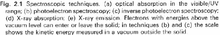
19 The Photoelectric Effect Albert Einstein considered electromagnetic energy to be bundled into little packets called photons. Energy of photon = E = hv Where, h = Planck constant ( 6.62 x J s ) v = frequency (Hz) of the radiation Photons of light hit surface electrons and transfer their energy hv = B.E. + K.E. hv e - (K.E.) The energized electrons overcome their attraction and escape from the surface Photoelectron spectroscopy detects the kinetic energy of the electron escaped from the surface. 19
20 20
21 Photoelectron spectroscopy -a single photon in/ electron out process X-ray Photoelectron Spectroscopy (XPS) - using soft x-ray ( ev) radiation to examine core-levels. Ultraviolet Photoelectron Spectroscopy (UPS) - using vacuum UV (10-45 ev) radiation to examine valence levels. 21
22 He(I) UPS spectrum of HCl gas. 1. Loss of a bonding electron decreases the bond order, increasing the bond length in the resulting cation compared to the parent molecule. 2. Loss of a nonbonding electron has no effect on bond order or bond length. 3. Loss of an antibonding electron increases the bond order, decreasing the bond length of the cation compared to the parent molecule. 22
23 E Peak shift- charging effect Broadening- molecular solid bonding and relaxation effects. 23
24 Metal oxides Eg Decrease in overlapping of the d-orbitals 24


25 Overlapping of d-orbitals of early transition metal elements in the Oxide structures Energy level diagram of early transition metal elements in the Oxide structures 25
26 Total density of states for NbO.The Fermi level corresponds to a d 3 electron count. 26

27 Metal sulfides semiconductor metallic 27

28 Density-functional studies of tungsten trioxide, tungsten bronzes, and related systems Physics, 2005, vol. 1 28
29 29
30 FIG. 8: Band structure diagrams of (a) cubic WO 3 and (b) NaWO 3. 30
31 FIG. 7: Calculated density of states for cubic tungsten bronzes, MWO3, near the Fermi level: (a) WO3, (b) HWO3, (c) LiWO3, (d) NaWO3, (e) KWO3, (f) RbWO3, (g) CsWO3. The Fermi level is indicated in each case. 31
32 32
33 Electrochromic material - color change by applying electric field semiconducting metallic Figure 1: The color of Na x WO 3 with different x values (degree of reduction of W). 33
34 The measurement of absorption edge and band gap properties of novel nanocomposite materials T. Nguyena, A. R. Hind, Varian Australia crystalline phases of TiO 2 - anatase, rutile, brookite layered titanates -K 2 Ti 3 O 7, K 2 Ti 4 O 9 34
 2 Ti 4 O 9 and (e) (Fe 3 (CH 3 COO) 7 OH)Ti 4 O 9. Absorption edges and band gap energies of nanocomposites and precursors.")
35 Diffuse reflectance spectra of nanocomposite materials: (a) TiO 2, (b) K 2 Ti 4 O 9, (c) (C 3 H 7 NH 3 ) 2 Ti 4 O 9, (d) C 6 H 12 (NH 3 ) 2 Ti 4 O 9 and (e) (Fe 3 (CH 3 COO) 7 OH)Ti 4 O 9. Absorption edges and band gap energies of nanocomposites and precursors. 35

36 36
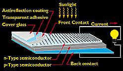
37 37
38 Titanium(IV) Oxide - properties high refractive index (n > 2.5, comparing to 1.45 of SiO 2 ) - pigments - photonic crystals n-type semiconductor (Eg ~ 3.2 ev) - photocatalysts reducible center - catalysts or catalyst supports 38
39 Photocatalysis over a Semiconductor Oxide such as TiO 2 Band gap of TiO 2 ~ 3.2 ev Amy Linsebigler et al., Chem. Rev., 95, 735,
40 O 2 (ads) TiO hν 2 h + + e - O -. H + 2. OOH H 2 O O 2.-. OH hν H 2 O 2 + H. - OOH + O 2 Scheme II Possible pathways for formation of hydroxy radical. 40

41 Electronic Band Structure of Titania Semiconductor Nanosheets Revealed by Electrochemical and Photoelectrochemical Studies J. AM. CHEM. SOC. 2004, 126,
42 42
 Current flows (forward bias) 43")
43 p- n junction Excess excess electron hole No current flows (reverse bias) Current flows (forward bias) 43
44 44
45 Photovoltaic Cell A photovoltaic cell, or solar cell, is a semiconductor device that converts light to electricity. The cell consists of a thin layer of p-type semiconductor, such as Si doped with Al, in contact with an n-type semiconductor, such as Si doped with P. The p-type semiconductor in the solar cell must be very thin - about 1 x 10⁻⁴ cm (1 µm), to reduce the tendency for conduction electrons produced by sunlight to be captured by positive holes and immobilized in covalent bonds. 45
46 Photovoltaic Cell 46

47 PV Connected to Utilities This electric vehicle recharging station in southern Florida is powered by a grid-connected PV array mounted on the roof. When no vehicles need charging, power from the modules is transferred to the utility line. (Photo: University of South Florida) 47


48 Simple PV Systems PV with Battery Storage 48
 and virtually all communications satellites are powered by")
49 PV in Space PV cells and modules are very reliable in space and on the earth. The Hubble space telescope (pictured here) and virtually all communications satellites are powered by photovoltaic technology. 49
50 Efficiencies of Various PV Cells Type of Solar cell Silicon III-V, II-VI Organic Compounds Semiconductor Efficiency Crystalline Single crystal 10~14% Si (disc) polycrystals 9~12% Amorphous a-si a-sio a-sige 6~9% Si 2 elements GaAs disc 18~30% CdS CdTe film 10~12% 3 elements CuInSe film 10~12% < 1% 50


51 Single crystal Si Polycrystalline Si Amorphous Si 51

52 Solar Spectrum Visible Large Area Pulsed Solar Simulator 52
 held clues to the potential new solar cell material by W.")
53 In search of better efficient Semiconductors Light emitting diodes (LED) made of indium gallium nitride (Eg = 0.7 ~ 3.4 ev) held clues to the potential new solar cell material by W. Walukiewicz at Berkerly 53
 covers the full solar spectrum")
54 A newly established indium gallium nitride system of alloys (In 1-x Ga x N) covers the full solar spectrum 54
Two-dimensional lattice
 1 Two-dimensional lattice a 1 *, k x k x = 0, k y = 0 X M a 2, y a 1, x Γ X a 2 *, k y k x = 0.5 a 1 *, k y = 0 k x = 0, k y = 0.5 a 2 * Γ k x = 0.5 a 1 *, k y = 0.5 a 2 * X X M k x = 0.25 a 1 *, k y =
1 Review of semiconductor materials and physics
 Part One Devices 1 Review of semiconductor materials and physics 1.1 Executive summary Semiconductor devices are fabricated using specific materials that offer the desired physical properties. There are
Chapter 1 Overview of Semiconductor Materials and Physics
 Chapter 1 Overview of Semiconductor Materials and Physics Professor Paul K. Chu Conductivity / Resistivity of Insulators, Semiconductors, and Conductors Semiconductor Elements Period II III IV V VI 2 B
ELEMENTARY BAND THEORY
 ELEMENTARY BAND THEORY PHYSICIST Solid state band Valence band, VB Conduction band, CB Fermi energy, E F Bloch orbital, delocalized n-doping p-doping Band gap, E g Direct band gap Indirect band gap Phonon
Electrons are shared in covalent bonds between atoms of Si. A bound electron has the lowest energy state.
 Photovoltaics Basic Steps the generation of light-generated carriers; the collection of the light-generated carriers to generate a current; the generation of a large voltage across the solar cell; and
Energy Spectroscopy. Excitation by means of a probe
 Energy Spectroscopy Excitation by means of a probe Energy spectral analysis of the in coming particles -> XAS or Energy spectral analysis of the out coming particles Different probes are possible: Auger
EE 5344 Introduction to MEMS CHAPTER 5 Radiation Sensors
 EE 5344 Introduction to MEMS CHAPTER 5 Radiation Sensors 5. Radiation Microsensors Radiation µ-sensors convert incident radiant signals into standard electrical out put signals. Radiant Signals Classification
Chapter 7. Solar Cell
 Chapter 7 Solar Cell 7.0 Introduction Solar cells are useful for both space and terrestrial application. Solar cells furnish the long duration power supply for satellites. It converts sunlight directly
Designing Information Devices and Systems II A. Sahai, J. Roychowdhury, K. Pister Discussion 1A
 EECS 16B Spring 2019 Designing Information Devices and Systems II A. Sahai, J. Roychowdhury, K. Pister Discussion 1A 1 Semiconductor Physics Generally, semiconductors are crystalline solids bonded into
Chemistry Instrumental Analysis Lecture 8. Chem 4631
 Chemistry 4631 Instrumental Analysis Lecture 8 UV to IR Components of Optical Basic components of spectroscopic instruments: stable source of radiant energy transparent container to hold sample device
So why is sodium a metal? Tungsten Half-filled 5d band & half-filled 6s band. Insulators. Interaction of metals with light?
 Bonding in Solids: Metals, Insulators, & CHEM 107 T. Hughbanks Delocalized bonding in Solids Think of a pure solid as a single, very large molecule. Use our bonding pictures to try to understand properties.
EE 446/646 Photovoltaic Devices I. Y. Baghzouz
 EE 446/646 Photovoltaic Devices I Y. Baghzouz What is Photovoltaics? First used in about 1890, the word has two parts: photo, derived from the Greek word for light, volt, relating to electricity pioneer
Bohr s Model, Energy Bands, Electrons and Holes
 Dual Character of Material Particles Experimental physics before 1900 demonstrated that most of the physical phenomena can be explained by Newton's equation of motion of material particles or bodies and
Basic cell design. Si cell
 Basic cell design Si cell 1 Concepts needed to describe photovoltaic device 1. energy bands in semiconductors: from bonds to bands 2. free carriers: holes and electrons, doping 3. electron and hole current:
Photocatalysis: semiconductor physics
 Photocatalysis: semiconductor physics Carlos J. Tavares Center of Physics, University of Minho, Portugal ctavares@fisica.uminho.pt www.fisica.uminho.pt 1 Guimarães Where do I come from? 3 Guimarães 4 Introduction>>
Ga and P Atoms to Covalent Solid GaP
 Ga and P Atoms to Covalent Solid GaP Band Gaps in Binary Group III-V Semiconductors Mixed Semiconductors Affect of replacing some of the As with P in GaAs Band Gap (ev) (nm) GaAs 1.35 919 (IR) GaP 2.24
Semiconductor Device Physics
 1 Semiconductor Device Physics Lecture 1 http://zitompul.wordpress.com 2 0 1 3 2 Semiconductor Device Physics Textbook: Semiconductor Device Fundamentals, Robert F. Pierret, International Edition, Addison
per unit cell Motif: Re at (0, 0, 0); 3O at ( 1 / 2, 0), (0, 0, 1 / 2 ) Re: 6 (octahedral coordination) O: 2 (linear coordination) ReO 6
; 3O at ( 1 / 2, 0), (0, 0, 1 / 2 ) Re: 6 (octahedral coordination) O: 2 (linear coordination) ReO 6") Lattice: Primitive Cubic 1ReO 3 per unit cell Motif: Re at (0, 0, 0); 3O at ( 1 / 2, 0, 0), (0, 1 / 2, 0), (0, 0, 1 / 2 ) Re: 6 (octahedral coordination) O: 2 (linear coordination) ReO 6 octahedra share
Lattice: Primitive Cubic 1ReO 3 per unit cell Motif: Re at (0, 0, 0); 3O at ( 1 / 2, 0, 0), (0, 1 / 2, 0), (0, 0, 1 / 2 ) Re: 6 (octahedral coordination) O: 2 (linear coordination) ReO 6 octahedra share
Atoms? All matters on earth made of atoms (made up of elements or combination of elements).
.") Chapter 1 Atoms? All matters on earth made of atoms (made up of elements or combination of elements). Atomic Structure Atom is the smallest particle of an element that can exist in a stable or independent
Chapter 1 Atoms? All matters on earth made of atoms (made up of elements or combination of elements). Atomic Structure Atom is the smallest particle of an element that can exist in a stable or independent
ELECTRONIC DEVICES AND CIRCUITS SUMMARY
 ELECTRONIC DEVICES AND CIRCUITS SUMMARY Classification of Materials: Insulator: An insulator is a material that offers a very low level (or negligible) of conductivity when voltage is applied. Eg: Paper,
Essentials of Quantum Physics
 Essentials of Quantum Physics References Direct energy conversion by S.W. Angrist, Ch 3. (out of print text book) Essential Quantum Physics by Peter Landshoff, Allen Metherell and Gareth Rees, 1997, Cambridge
Diamond. Covalent Insulators and Semiconductors. Silicon, Germanium, Gray Tin. Chem 462 September 24, 2004
 Covalent Insulators and Chem 462 September 24, 2004 Diamond Pure sp 3 carbon All bonds staggered- ideal d(c-c) - 1.54 Å, like ethane Silicon, Germanium, Gray Tin Diamond structure Si and Ge: semiconductors
electronics fundamentals
 electronics fundamentals circuits, devices, and applications THOMAS L. FLOYD DAVID M. BUCHLA Lesson 1: Diodes and Applications Semiconductors Figure 1-1 The Bohr model of an atom showing electrons in orbits
EE143 Fall 2016 Microfabrication Technologies. Evolution of Devices
 EE143 Fall 2016 Microfabrication Technologies Prof. Ming C. Wu wu@eecs.berkeley.edu 511 Sutardja Dai Hall (SDH) 1-1 Evolution of Devices Yesterday s Transistor (1947) Today s Transistor (2006) 1-2 1 Why
Chem 481 Lecture Material 3/20/09
 Chem 481 Lecture Material 3/20/09 Radiation Detection and Measurement Semiconductor Detectors The electrons in a sample of silicon are each bound to specific silicon atoms (occupy the valence band). If
Introduction to Photovoltaics
 INTRODUCTION Objectives Understand the photovoltaic effect. Understand the properties of light. Describe frequency and wavelength. Understand the factors that determine available light energy. Use software
EECS143 Microfabrication Technology
 EECS143 Microfabrication Technology Professor Ali Javey Introduction to Materials Lecture 1 Evolution of Devices Yesterday s Transistor (1947) Today s Transistor (2006) Why Semiconductors? Conductors e.g
Chapter 4: Bonding in Solids and Electronic Properties. Free electron theory
 Chapter 4: Bonding in Solids and Electronic Properties Free electron theory Consider free electrons in a metal an electron gas. regards a metal as a box in which electrons are free to move. assumes nuclei
Photovoltaic Energy Conversion. Frank Zimmermann
 Photovoltaic Energy Conversion Frank Zimmermann Solar Electricity Generation Consumes no fuel No pollution No greenhouse gases No moving parts, little or no maintenance Sunlight is plentiful & inexhaustible
Lecture 18: Semiconductors - continued (Kittel Ch. 8)
") Lecture 18: Semiconductors - continued (Kittel Ch. 8) + a - Donors and acceptors J U,e e J q,e Transport of charge and energy h E J q,e J U,h Physics 460 F 2006 Lect 18 1 Outline More on concentrations
Lecture 18: Semiconductors - continued (Kittel Ch. 8) + a - Donors and acceptors J U,e e J q,e Transport of charge and energy h E J q,e J U,h Physics 460 F 2006 Lect 18 1 Outline More on concentrations
Engineering 2000 Chapter 8 Semiconductors. ENG2000: R.I. Hornsey Semi: 1
 Engineering 2000 Chapter 8 Semiconductors ENG2000: R.I. Hornsey Semi: 1 Overview We need to know the electrical properties of Si To do this, we must also draw on some of the physical properties and we
Energy Spectroscopy. Ex.: Fe/MgO
 Energy Spectroscopy Spectroscopy gives access to the electronic properties (and thus chemistry, magnetism,..) of the investigated system with thickness dependence Ex.: Fe/MgO Fe O Mg Control of the oxidation
1 Name: Student number: DEPARTMENT OF PHYSICS AND PHYSICAL OCEANOGRAPHY MEMORIAL UNIVERSITY OF NEWFOUNDLAND. Fall :00-11:00
 1 Name: DEPARTMENT OF PHYSICS AND PHYSICAL OCEANOGRAPHY MEMORIAL UNIVERSITY OF NEWFOUNDLAND Final Exam Physics 3000 December 11, 2012 Fall 2012 9:00-11:00 INSTRUCTIONS: 1. Answer all seven (7) questions.
PHYSICS nd TERM Outline Notes (continued)
") PHYSICS 2800 2 nd TERM Outline Notes (continued) Section 6. Optical Properties (see also textbook, chapter 15) This section will be concerned with how electromagnetic radiation (visible light, in particular)
PHYSICS 2800 2 nd TERM Outline Notes (continued) Section 6. Optical Properties (see also textbook, chapter 15) This section will be concerned with how electromagnetic radiation (visible light, in particular)
Electron Energy, E E = 0. Free electron. 3s Band 2p Band Overlapping energy bands. 3p 3s 2p 2s. 2s Band. Electrons. 1s ATOM SOLID.
 Electron Energy, E Free electron Vacuum level 3p 3s 2p 2s 2s Band 3s Band 2p Band Overlapping energy bands Electrons E = 0 1s ATOM 1s SOLID In a metal the various energy bands overlap to give a single
Modern Physics for Frommies IV The Universe - Small to Large Lecture 4
 Fromm Institute for Lifelong Learning University of San Francisco Modern Physics for Frommies IV The Universe - Small to Large Lecture 4 3 February 06 Modern Physics IV Lecture 4 Agenda Administrative
Electronics The basics of semiconductor physics
 Electronics The basics of semiconductor physics Prof. Márta Rencz, Gergely Nagy BME DED September 16, 2013 The basic properties of semiconductors Semiconductors conductance is between that of conductors
Lecture 1. OUTLINE Basic Semiconductor Physics. Reading: Chapter 2.1. Semiconductors Intrinsic (undoped) silicon Doping Carrier concentrations
 silicon Doping Carrier concentrations") Lecture 1 OUTLINE Basic Semiconductor Physics Semiconductors Intrinsic (undoped) silicon Doping Carrier concentrations Reading: Chapter 2.1 EE105 Fall 2007 Lecture 1, Slide 1 What is a Semiconductor? Low
Lecture 1 OUTLINE Basic Semiconductor Physics Semiconductors Intrinsic (undoped) silicon Doping Carrier concentrations Reading: Chapter 2.1 EE105 Fall 2007 Lecture 1, Slide 1 What is a Semiconductor? Low
CLASS 12th. Semiconductors
 CLASS 12th Semiconductors 01. Distinction Between Metals, Insulators and Semi-Conductors Metals are good conductors of electricity, insulators do not conduct electricity, while the semiconductors have
Birck Nanotechnology Center XPS: X-ray Photoelectron Spectroscopy ESCA: Electron Spectrometer for Chemical Analysis
 Birck Nanotechnology Center XPS: X-ray Photoelectron Spectroscopy ESCA: Electron Spectrometer for Chemical Analysis Dmitry Zemlyanov Birck Nanotechnology Center, Purdue University Outline Introduction
Introduction to Semiconductor Physics. Prof.P. Ravindran, Department of Physics, Central University of Tamil Nadu, India
 Introduction to Semiconductor Physics 1 Prof.P. Ravindran, Department of Physics, Central University of Tamil Nadu, India http://folk.uio.no/ravi/cmp2013 Review of Semiconductor Physics Semiconductor fundamentals
A semiconductor is an almost insulating material, in which by contamination (doping) positive or negative charge carriers can be introduced.
 positive or negative charge carriers can be introduced.") Semiconductor A semiconductor is an almost insulating material, in which by contamination (doping) positive or negative charge carriers can be introduced. Page 2 Semiconductor materials Page 3 Energy levels
Semiconductor A semiconductor is an almost insulating material, in which by contamination (doping) positive or negative charge carriers can be introduced. Page 2 Semiconductor materials Page 3 Energy levels
Unit IV Semiconductors Engineering Physics
 Introduction A semiconductor is a material that has a resistivity lies between that of a conductor and an insulator. The conductivity of a semiconductor material can be varied under an external electrical
smal band gap Saturday, April 9, 2011
 small band gap upper (conduction) band empty small gap valence band filled 2s 2p 2s 2p hybrid (s+p)band 2p no gap 2s (depend on the crystallographic orientation) extrinsic semiconductor semi-metal electron
Chap 10 Part 3a.notebook December 12, 2017
 Metallic Bonding and Semiconductors Chapter 10 Sect 4 Metallic Bonding positive metal ions surrounded by a "sea of electrons" Bonding is strong and nondirectional Iron, Silver, alloys, Brass, Bronze Forces
Nearly Free Electron Gas model - II
 Nearly Free Electron Gas model - II Contents 1 Lattice scattering 1 1.1 Bloch waves............................ 2 1.2 Band gap formation........................ 3 1.3 Electron group velocity and effective
LN 3 IDLE MIND SOLUTIONS
 IDLE MIND SOLUTIONS 1. Let us first look in most general terms at the optical properties of solids with band gaps (E g ) of less than 4 ev, semiconductors by definition. The band gap energy (E g ) can
Photovoltaic cell and module physics and technology
 Photovoltaic cell and module physics and technology Vitezslav Benda, Prof Czech Technical University in Prague benda@fel.cvut.cz www.fel.cvut.cz 6/21/2012 1 Outlines Photovoltaic Effect Photovoltaic cell
Solid State Device Fundamentals
 Solid State Device Fundamentals ENS 345 Lecture Course by Alexander M. Zaitsev alexander.zaitsev@csi.cuny.edu Tel: 718 982 2812 Office 4N101b 1 The free electron model of metals The free electron model
3.1 Absorption and Transparency
 3.1 Absorption and Transparency 3.1.1 Optical Devices (definitions) 3.1.2 Photon and Semiconductor Interactions 3.1.3 Photon Intensity 3.1.4 Absorption 3.1 Absorption and Transparency Objective 1: Recall
EE495/695 Introduction to Semiconductors I. Y. Baghzouz ECE Department UNLV
 EE495/695 Introduction to Semiconductors I Y. Baghzouz ECE Department UNLV Introduction Solar cells have always been aligned closely with other electronic devices. We will cover the basic aspects of semiconductor
Fabrication Technology, Part I
 EEL5225: Principles of MEMS Transducers (Fall 2004) Fabrication Technology, Part I Agenda: Microfabrication Overview Basic semiconductor devices Materials Key processes Oxidation Thin-film Deposition Reading:
Conductivity and Semi-Conductors
 Conductivity and Semi-Conductors J = current density = I/A E = Electric field intensity = V/l where l is the distance between two points Metals: Semiconductors: Many Polymers and Glasses 1 Electrical Conduction
Photovoltaic cell and module physics and technology. Vitezslav Benda, Prof Czech Technical University in Prague
 Photovoltaic cell and module physics and technology Vitezslav Benda, Prof Czech Technical University in Prague benda@fel.cvut.cz www.fel.cvut.cz 1 Outlines Photovoltaic Effect Photovoltaic cell structure
EECS130 Integrated Circuit Devices
 EECS130 Integrated Circuit Devices Professor Ali Javey 8/30/2007 Semiconductor Fundamentals Lecture 2 Read: Chapters 1 and 2 Last Lecture: Energy Band Diagram Conduction band E c E g Band gap E v Valence
PHOTOVOLTAICS Fundamentals
 PHOTOVOLTAICS Fundamentals PV FUNDAMENTALS Semiconductor basics pn junction Solar cell operation Design of silicon solar cell SEMICONDUCTOR BASICS Allowed energy bands Valence and conduction band Fermi
Lecture 1. Introduction to Electronic Materials. Reading: Pierret 1.1, 1.2, 1.4,
 Lecture 1 Introduction to Electronic Materials Reading: Pierret 1.1, 1.2, 1.4, 2.1-2.6 Atoms to Operational Amplifiers The goal of this course is to teach the fundamentals of non-linear circuit elements
3.1 Introduction to Semiconductors. Y. Baghzouz ECE Department UNLV
 3.1 Introduction to Semiconductors Y. Baghzouz ECE Department UNLV Introduction In this lecture, we will cover the basic aspects of semiconductor materials, and the physical mechanisms which are at the
A SEMICONDUCTOR DIODE. P-N Junction
 A SEMICONDUCTOR DIODE P-N Junction Analog Electronics Pujianto Department of Physics Edu. State University of Yogyakarta A Semiconductor Devices A Semiconductor devices can be defined as a unit which consists,
Qualitative Picture of the Ideal Diode. G.R. Tynan UC San Diego MAE 119 Lecture Notes
 Qualitative Picture of the Ideal Diode G.R. Tynan UC San Diego MAE 119 Lecture Notes Band Theory of Solids: From Single Attoms to Solid Crystals Isolated Li atom (conducting metal) Has well-defined, isolated
ENERGY BANDS AND GAPS IN SEMICONDUCTOR. Muhammad Hafeez Javed
 ENERGY BANDS AND GAPS IN SEMICONDUCTOR Muhammad Hafeez Javed www.rmhjaved.com rmhjaved@gmail.com Out Line Introduction Energy band Classification of materials Direct and indirect band gap of SC Classification
REFRACTORY METAL OXIDES: FABRICATION OF NANOSTRUCTURES, PROPERTIES AND APPLICATIONS
 REFRACTORY METAL OXIDES: FABRICATION OF NANOSTRUCTURES, PROPERTIES AND APPLICATIONS S.K. Lazarouk, D.A. Sasinovich BELARUSIAN STATE UNIVERSITY OF INFORMATICS AND RADIOELECTRONICS Outline: -- experimental
Introduction to X-ray Photoelectron Spectroscopy (XPS) XPS which makes use of the photoelectric effect, was developed in the mid-1960
 XPS which makes use of the photoelectric effect, was developed in the mid-1960") Introduction to X-ray Photoelectron Spectroscopy (XPS) X-ray Photoelectron Spectroscopy (XPS), also known as Electron Spectroscopy for Chemical Analysis (ESCA) is a widely used technique to investigate
Introduction to X-ray Photoelectron Spectroscopy (XPS) X-ray Photoelectron Spectroscopy (XPS), also known as Electron Spectroscopy for Chemical Analysis (ESCA) is a widely used technique to investigate
Introduction CHAPTER 01. Light and opto-semiconductors. Opto-semiconductor lineup. Manufacturing process of opto-semiconductors.
 CHAPTER 0 Light and opto-semiconductors - -2 Light Opto-semiconductors P. 0 P. 3 2 Opto-semiconductor lineup P. 5 3 Manufacturing process of opto-semiconductors P. 6 9 CHAPTER 0. Light and opto-semiconductors
Misan University College of Engineering Electrical Engineering Department. Exam: Final semester Date: 17/6/2017
 Misan University College of Engineering Electrical Engineering Department Subject: Electronic I Class: 1 st stage Exam: Final semester Date: 17/6/2017 Examiner: Dr. Baqer. O. TH. Time: 3 hr. Note: Answer
ET3034TUx Utilization of band gap energy
 ET3034TUx - 3.3.1 - Utilization of band gap energy In the last two weeks we have discussed the working principle of a solar cell and the external parameters that define the performance of a solar cell.
Semiconductors and Optoelectronics. Today Semiconductors Acoustics. Tomorrow Come to CH325 Exercises Tours
 Semiconductors and Optoelectronics Advanced Physics Lab, PHYS 3600 Don Heiman, Northeastern University, 2017 Today Semiconductors Acoustics Tomorrow Come to CH325 Exercises Tours Semiconductors and Optoelectronics
Semiconductors. Semiconductors also can collect and generate photons, so they are important in optoelectronic or photonic applications.
 Semiconductors Semiconducting materials have electrical properties that fall between true conductors, (like metals) which are always highly conducting and insulators (like glass or plastic or common ceramics)
EE301 Electronics I , Fall
 EE301 Electronics I 2018-2019, Fall 1. Introduction to Microelectronics (1 Week/3 Hrs.) Introduction, Historical Background, Basic Consepts 2. Rewiev of Semiconductors (1 Week/3 Hrs.) Semiconductor materials
The electronic structure of solids. Charge transport in solids
 The electronic structure of solids We need a picture of the electronic structure of solid that we can use to explain experimental observations and make predictions Why is diamond an insulator? Why is sodium
6. Computational Design of Energy-related Materials
 6. Computational Design of Energy-related Materials Contents 6.1 Atomistic Simulation Methods for Energy Materials 6.2 ab initio design of photovoltaic materials 6.3 Solid Ion Conductors for Fuel Cells
1.4 Crystal structure
 1.4 Crystal structure (a) crystalline vs. (b) amorphous configurations short and long range order only short range order Abbildungen: S. Hunklinger, Festkörperphysik, Oldenbourg Verlag represenatives of
Chap. 11 Semiconductor Diodes
 Chap. 11 Semiconductor Diodes Semiconductor diodes provide the best resolution for energy measurements, silicon based devices are generally used for charged-particles, germanium for photons. Scintillators
Module 6 : PHYSICS OF SEMICONDUCTOR DEVICES Lecture 32 : Bonding in Solids
 Module 6 : PHYSICS OF SEMICONDUCTOR DEVICES Lecture 32 : Bonding in Solids Objectives In this course you will learn the following Bonding in solids. Ionic and covalent bond. Structure of Silicon Concept
Classification of Solids
 Classification of Solids Classification by conductivity, which is related to the band structure: (Filled bands are shown dark; D(E) = Density of states) Class Electron Density Density of States D(E) Examples
Class XII_All India_Physics_Set-2
 Class XII_All India_Physics_Set- 17. Draw V I characteristics of a p-n junction diode. Answer the following questions, giving reasons: (i) Why is the current under reverse bias almost independent of the
Photon Interaction. Spectroscopy
 Photon Interaction Incident photon interacts with electrons Core and Valence Cross Sections Photon is Adsorbed Elastic Scattered Inelastic Scattered Electron is Emitted Excitated Dexcitated Stöhr, NEXAPS
e - Galvanic Cell 1. Voltage Sources 1.1 Polymer Electrolyte Membrane (PEM) Fuel Cell
 Fuel Cell") Galvanic cells convert different forms of energy (chemical fuel, sunlight, mechanical pressure, etc.) into electrical energy and heat. In this lecture, we are interested in some examples of galvanic cells.
Galvanic cells convert different forms of energy (chemical fuel, sunlight, mechanical pressure, etc.) into electrical energy and heat. In this lecture, we are interested in some examples of galvanic cells.
EE130: Integrated Circuit Devices
 EE130: Integrated Circuit Devices (online at http://webcast.berkeley.edu) Instructor: Prof. Tsu-Jae King (tking@eecs.berkeley.edu) TA s: Marie Eyoum (meyoum@eecs.berkeley.edu) Alvaro Padilla (apadilla@eecs.berkeley.edu)
4.2 Molecular orbitals and atomic orbitals Consider a linear chain of four identical atoms representing a hypothetical molecule.
 4. Molecular orbitals and atomic orbitals Consider a linear chain of four identical atoms representing a hypothetical molecule. Suppose that each atomic wavefunction is 1s wavefunction. This system of
Molecular Orbital Theory
 Molecular Orbital Theory 1. MO theory suggests that atomic orbitals of different atoms combine to create MOLECULAR ORBITALS 2. Electrons in these MOLECULAR ORBITALS belong to the molecule as whole 3. This
Lecture 2. Semiconductor Physics. Sunday 4/10/2015 Semiconductor Physics 1-1
 Lecture 2 Semiconductor Physics Sunday 4/10/2015 Semiconductor Physics 1-1 Outline Intrinsic bond model: electrons and holes Charge carrier generation and recombination Intrinsic semiconductor Doping:
ELEC 4700 Assignment #2
 ELEC 4700 Assignment #2 Question 1 (Kasop 4.2) Molecular Orbitals and Atomic Orbitals Consider a linear chain of four identical atoms representing a hypothetical molecule. Suppose that each atomic wavefunction
X-Ray Photoelectron Spectroscopy (XPS)
") X-Ray Photoelectron Spectroscopy (XPS) Louis Scudiero http://www.wsu.edu/~scudiero; 5-2669 Electron Spectroscopy for Chemical Analysis (ESCA) The basic principle of the photoelectric effect was enunciated
X-Ray Photoelectron Spectroscopy (XPS) Louis Scudiero http://www.wsu.edu/~scudiero; 5-2669 Electron Spectroscopy for Chemical Analysis (ESCA) The basic principle of the photoelectric effect was enunciated
Basic Semiconductor Physics
 6 Basic Semiconductor Physics 6.1 Introduction With this chapter we start with the discussion of some important concepts from semiconductor physics, which are required to understand the operation of solar
CME 300 Properties of Materials. ANSWERS: Homework 9 November 26, As atoms approach each other in the solid state the quantized energy states:
 CME 300 Properties of Materials ANSWERS: Homework 9 November 26, 2011 As atoms approach each other in the solid state the quantized energy states: are split. This splitting is associated with the wave
Advantages / Disadvantages of semiconductor detectors
 Advantages / Disadvantages of semiconductor detectors Semiconductor detectors have a high density (compared to gas detector) large energy loss in a short distance diffusion effect is smaller than in gas
Where are we? Check-In
 Where are we? Check-In ü Building Blocks of Matter ü Moles, molecules, grams, gases, ü The Bohr Model solutions, and percent composition Coulomb s Law ü Empirical and Molecular formulas Photoelectron Spectroscopy
Metallic & Ionic Solids. Crystal Lattices. Properties of Solids. Network Solids. Types of Solids. Chapter 13 Solids. Chapter 13
 1 Metallic & Ionic Solids Chapter 13 The Chemistry of Solids Jeffrey Mack California State University, Sacramento Crystal Lattices Properties of Solids Regular 3-D arrangements of equivalent LATTICE POINTS
The design of an integrated XPS/Raman spectroscopy instrument for co-incident analysis
 The design of an integrated XPS/Raman spectroscopy instrument for co-incident analysis Tim Nunney The world leader in serving science 2 XPS Surface Analysis XPS +... UV Photoelectron Spectroscopy UPS He(I)
Free Electron Model for Metals
 Free Electron Model for Metals Metals are very good at conducting both heat and electricity. A lattice of in a sea of electrons shared between all nuclei (moving freely between them): This is referred
Nanotechnology and Solar Energy. Solar Electricity Photovoltaics. Fuel from the Sun Photosynthesis Biofuels Split Water Fuel Cells
 Nanotechnology and Solar Energy Solar Electricity Photovoltaics Fuel from the Sun Photosynthesis Biofuels Split Water Fuel Cells Solar cell A photon from the Sun generates an electron-hole pair in a semiconductor.
KATIHAL FİZİĞİ MNT-510
 KATIHAL FİZİĞİ MNT-510 YARIİLETKENLER Kaynaklar: Katıhal Fiziği, Prof. Dr. Mustafa Dikici, Seçkin Yayıncılık Katıhal Fiziği, Şakir Aydoğan, Nobel Yayıncılık, Physics for Computer Science Students: With
I. Introduction II. Solid State Physics Detection of Light Bernhard Brandl 1
 Detection of Light I. Introduction II. Solid State Physics 4-2-2015 Detection of Light Bernhard Brandl 1 4-2-2015 Detection of Light Bernhard Brandl 2 Blabla Recommended 4-2-2015 Detection of Light Bernhard
Week 13 MO Theory, Solids, & metals
 Week 13 MO Theory, Solids, & metals Q UEST IO N 1 Using the molecular orbital energy diagrams below, which one of the following diatomic molecules is LEAST likely to exist? A. Li2 B. Be2 C. B2 D. C2 E.
Contents CONTENTS. Page 2 of 47
 J. A. Hargreaves Lockerbie Academy June 2015 Contents CONTENTS Contents... 2 CHAPTER 7 CONDUCTORS, SEMICONDUCTORS AND INSULATORS... 4 Summary of Content... 4 Summary of this chapter- notes from column
EEE4106Z Radiation Interactions & Detection
 EEE4106Z Radiation Interactions & Detection 2. Radiation Detection Dr. Steve Peterson 5.14 RW James Department of Physics University of Cape Town steve.peterson@uct.ac.za May 06, 2015 EEE4106Z :: Radiation
Semiconductor Physics and Devices
 Syllabus Advanced Nano Materials Semiconductor Physics and Devices Textbook Donald A. Neamen (McGraw-Hill) Semiconductor Physics and Devices Seong Jun Kang Department of Advanced Materials Engineering
Notes on Solids and Liquids
 THE LIQUID STATE Notes on Solids and Liquids Why do liquids tend to bead up when on a solid surface? The effect of uneven pull on surface molecules draws them into the body of the liquid causing droplet
Chapter 10: Modern Atomic Theory and the Periodic Table. How does atomic structure relate to the periodic table? 10.1 Electromagnetic Radiation
 Chapter 10: Modern Atomic Theory and the Periodic Table How does atomic structure relate to the periodic table? 10.1 Electromagnetic Radiation Electromagnetic (EM) radiation is a form of energy that exhibits