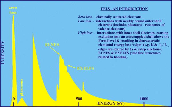
EELS Electron Energy Loss Spectroscopy
|
|
|
- Trevor Fleming
- 6 years ago
- Views:
Transcription

1 EELS Electron Energy Loss Spectroscopy (Thanks to Steve Pennycook, Quan Li, Charlie Lyman, Ondre Krivenak, David Muller, David Bell, Natasha Erdman, Nestor Zaluzec and many others)
2
3
4
5

6 Nestor Zaluzec, ANL
7 Nestor Zaluzec, ANL
8
9
10
11 Real Life FEG STEM at UIC
 Objective C S")
")

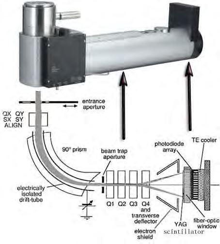
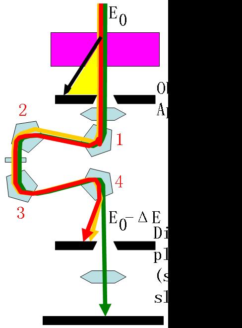
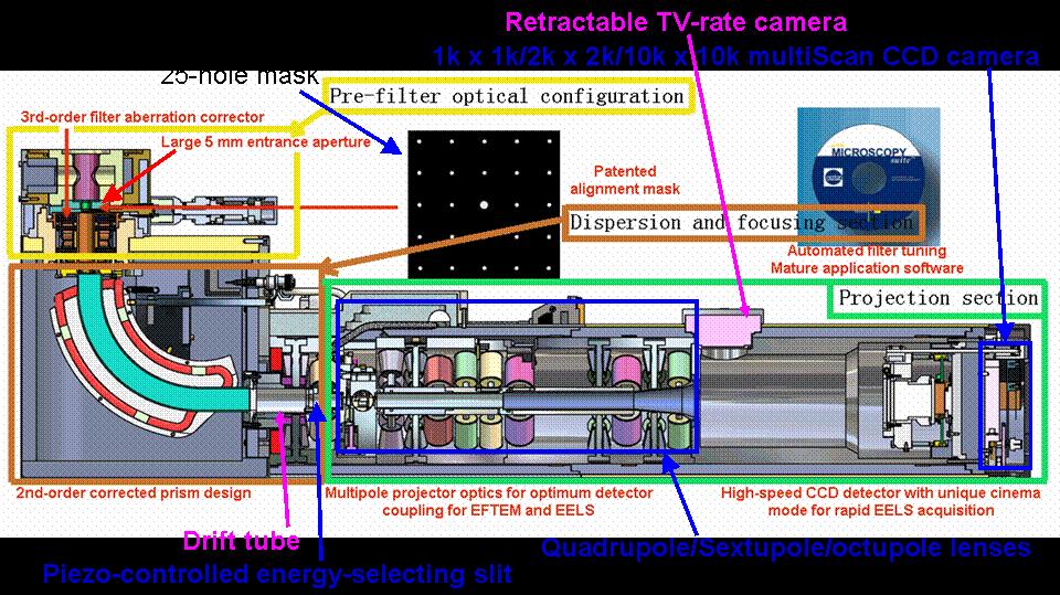
12 LIBRA 200 C s and Monochromator FEG Monochromator + Monochromator Condenser (C1, C2 & C3) Objective C S Corrector 20/09/ Projector 1 (P1, P2 & P3) Corrected Omega Filter Projector 2 (P4, P5 & P6) Viewing chamber + Detectors dispersive plane (slit) Dispersion free Ease of use 30% of intensity at 0.2eV M&M 2010 Portland
13
14 Energy Levels and Energy-Loss Spectrum from Williams and Carter, Transmission Electron Microscopy, Springer, 1996
15 Basic formalism Ignore diffraction effects, not really right but OK for now Consider inelastic scattering as completely incoherent 99% correct Ignore relativistic effects, not correct and over the last decade they have been shown to be critical Assume that processes are not dependent upon the electron energy, good for swift electrons Consider a simple probability P(dE,q), for de change in energy and q wavevector change Many simplifications if we integrate over all q, collection angle (experimental variable)
16 Basic formalism dddd EE,qq,zz dddd = II EE EE, qq qq, zz PP ddee, ddqq ddee dddd Simplest case when energies do not overlap leads to a Poisson distribution solution: II EE, qq, tt = exp tt λλ δδ(ee) + tttt dddd, qq exp tt λλ δδ EE dddd + II EE nnnnnn, nnnn, tt = ( 1 nn! )ttnn PP nn dddd, qq exp( tt/λλ) 1/λλ = PP dddd, qq dddddddd)) We call λ the mean free path. Note that the zero-loss peak has an intensity of exp(-t/λ), so if we divide by this we get tp(de,q) for single scattering With multiple scattering the result is slightly more complicated, but one can do a log deconvolution to clean up the data
17 Al specimen Plasmon Peaks Thin sample Thick sample Transmission Electron Microscopy by David B. Williams and C. Barry Carter, Plenum Press, New York, 1996.
18 Al free electron metal Fe Transition metal 1b Plasmon peak NiO ZrO 2 interface NiO ZrO 2 6 nm interface Transmission Electron Microscopy, David B. Williams & C. Barry Carter, Plenum Press, New York, 1996.
19 Inter- and Intra Band Transitions Spectra vertically displaced for easy visibility Energy-loss (ev) Low loss spectrum from Al and Al compounds The differences in the spectra are due to differences in bonding Transmission Electron Microscopy by David B. Williams and C. Barry Carter, Plenum Press, New York, 1996.
20 Band gap differences manifesting itself in the low loss region of the EELS spectrum 1a Low loss region before Plasmon peak Intraband transition characteristic of Polystyrene Transmission Electron Microscopy, David B. Williams & C. Barry Carter, Plenum Press, New York, 1996.
21 Core Losses bkgd Spectrum Bkgd Counts x 10^ L 3 L 2 L 1 Edge ev
22 Idealized edge Edge superimposed on plural scattering Bonding Effects ELNES EXELFS Diffraction Effects from atoms surrounding the ionized atom Thick Specimen Combination of ionization and plasmon losses Ionization loss Plasmon loss Transmission Electron Microscopy by David B. Williams and C. Barry Carter, Plenum Press, New York, 1996.
23 The L edge of transition metals
24 Chemical bonding Cu and CuO 3d 10 3p 6 3s 2 2p 6 2s 2 1s

25 eels.kuicr.kyoto-u.ac.jp/eels.en.html Diamond, graphite and fullerene all consist of only carbon. All of these specimens have absorption peaks around 284 ev in EELS corresponding to the existence of carbon atoms. From the fine structure of the absorption peak, the difference in bonding state and local electronic state can be detected. The sharp peak at absorption edge corresponds to the excitation of carbon K-shell electron (1s electron) to empty anti-bonding pi-orbital. It is not observed for diamond, because of no pi-electron in it.

26 Sliding on NFC Sliding Region Is low friction associated with π-bond formation? Merkle et al, Carbon, in press In-situ result: Yes J.C. Sanchez-Lopez et al., Surf. Coat. Tech. 163, 444 (2003)
27

28 FEI monochromator (Tiejmeier et al.)
29 Additional fine structure seen with monochromation Rez,2004:


30 Monochromator / Energy-Filter Performance FWHM= 600 mev No 200KV FWHM= 81 mev FWHM= 62 mev Monochromator 1um 200KV Monochromator 1um 80KV
31 Schematic of the Nion high resolution monochromator Full description in: Krivanek et al., Phil. Trans. R. Soc. A 367 (2009) un-dispersed outgoing beam EELS 1 energy-dispersed beam Energy dispersion at slit is variable from ~ 2 µm/ev to ~ 200 µm/ev EELS 2 monochromated beam incoming beam The Nion monochromator is equivalent to 2 parallel EEL spectrometers arranged back-to back, with an energy-selecting slit in the mid-plane, plus (next slide):


32 More recent zero loss peaks MC in final position, stabilization schemes not yet connected up. Stabilization scheme 1 connected, but not making much difference: short exposure time is needed to avoid broadening the ZLP. The instability is due to elements outside the stabilization scheme, e.g. the quadrupoles of the MC or the quads of the EELS. The probe on the sample does not jitter, and this points to the EELS as the source of the problem.


33 EELS spectra Ti L 2,3 TiC TiN Stainless steel specimen Transmission Electron Microscopy by David B. Williams and C. Barry Carter, Plenum Press, New York, 1996.


34 No visible Grain Boundary Å counts EELS Si peak at 1839 ev Sr L 2,3 peaks Grain Boundary ev Fourier filtered image Dislocation structures at the Grain boundary counts ev Grain ev ~8º TILT BOUNDARY IN THE SrTiO 3 POLYCRYSTAL VG microscope GB2 3x4 Dist 5 nm MX2 3x4

 Ti 0.")
35 Single B x S 1-x TO nanocubes EELS 7 nanocubes are detected as EELS, and the Ba/O= Ti/O= , X average value is close is 0.5. Relative quantification: Elem. Atomic ratio (/) Ti 0.33 ± O 1.00 ± Ba 0.15 ± 0.022
36 Three-window method Elemental mapping W3 / (W1 +W2) = Elemental map Window 1 Window 2 Window 3
37
38
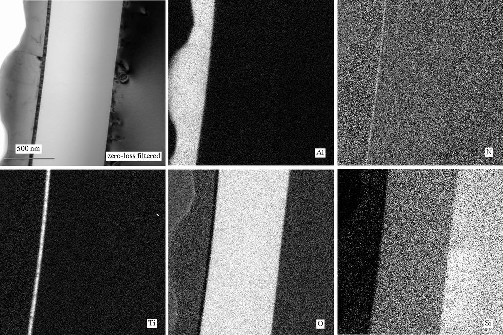
39 Multilayer coating

40 Carbon Nanotube
")


41 Electron Microscopy Methods for the Characterization of Nanomaterials (Example: Vanadium Oxide Nanotubes) SEM: characterization of tubular morphology EELS: composition V map C map Cross-sections of VO x nanotubes: TEM and elemental maps obtained by electron spectroscopic imaging TEM: characterization of the wall structure
42 Column-by-column Scanned Incident Probe Specimen EELS? Dynamical effects Beam broadening Localization Interpretation ADF Column by column image IBF = 1-ADF Prism Column by column EELS? EELS
 1 2 3 4 5 L-edge intensity (% of bulk) 1 0.8 0.6 0.4 0.2 0 CoSi 2 2.7 Å Theory Experiment Si 6 7 760 770 780 790 800 810 Energy (ev) -0.")
43 Atomic resolution chemical analysis Edge resolution test on CoSi 2 /Si(111) interface VG Microscopes HB501UX, 100 kv, ~ 2.2 Å probe 1.2 Counts (arbitrary units) L-edge intensity (% of bulk) CoSi Å Theory Experiment Si Energy (ev) Probe position by atomic plane Browning, Chisholm, Pennycook, Nature 1993
 095502 La-doped CaTiO 3 5 Å Annular Detector I Z 2 EELS Spectrometer Intensity La M 4,5 820 850 880 Energy (ev) EELS ~ XAS with")
44 Single Atom Spectroscopy Scanned Probe M. Varela, et al., Phys. Rev. Lett. 92 (2004) La-doped CaTiO 3 5 Å Annular Detector I Z 2 EELS Spectrometer Intensity La M 4, Energy (ev) EELS ~ XAS with atomic resolution and sensitivity to 1 atom ~ STM but below the surface

45 An example D. A. Muller, Nature 399, 58 (1999)
46
 and M. Varela (ORNL).")
47 Atomic resolution EELS and EDX Simultaneously acquired EELS and EDS maps from a LaFeO3/SrTiO3 interface. Principal component analysis was used to remove random noise. Data acquired in ajeol JEM-ARM200F at 200 kv, courtesy of E. Okunishi (JEOL) and M. Varela (ORNL). Sample courtesy of Jacobo Santamaria's group (Complutense University, Spain).

 Annular Bright")


48 Atomic resolution Imaging and EELS map with High Energy Resolution Ca 3 Co 4 O 9 (110) Annular Bright Field (ABF) EELS SI Ca Co O HAADF 0.5 nm Data courtesy of Dr. Robert Klie, University of Illinois at Chicago


, 161 165.")
49 Atom by atom spectroscopy survey ADF 2 Å Si-L C-K N-K N Si Zhou, W., Lee, J., Nanda, J., Pantelides, S. T., Pennycook, S. J., & Idrobo, J.- C. (2012). Atomically localized plasmon enhancement in monolayer graphene. Nature nanotechnology, 7(3), Materials Science and Engineering and Scientific User Facilities Divisions


50 Bonding of single Si atoms in the graphene lattice Si-C 4 Si-C 3 Some 3d states in Si-C 4 structure are missing!
51
52
53
Microscopy: Principles
 Low Voltage Electron Microscopy: Principles and Applications Edited by David C. Bell Harvard University, USA and Natasha Erdman JEOL USA Inc., USA Published in association with the Royal Microscopical
Chemical Analysis in TEM: XEDS, EELS and EFTEM. HRTEM PhD course Lecture 5
 Chemical Analysis in TEM: XEDS, EELS and EFTEM HRTEM PhD course Lecture 5 1 Part IV Subject Chapter Prio x-ray spectrometry 32 1 Spectra and mapping 33 2 Qualitative XEDS 34 1 Quantitative XEDS 35.1-35.4
IMAGING DIFFRACTION SPECTROSCOPY
 TEM Techniques TEM/STEM IMAGING DIFFRACTION SPECTROSCOPY Amplitude contrast (diffracion contrast) Phase contrast (highresolution imaging) Selected area diffraction Energy dispersive X-ray spectroscopy
Chapter 9. Electron mean free path Microscopy principles of SEM, TEM, LEEM
 Chapter 9 Electron mean free path Microscopy principles of SEM, TEM, LEEM 9.1 Electron Mean Free Path 9. Scanning Electron Microscopy (SEM) -SEM design; Secondary electron imaging; Backscattered electron
Energy-Filtering. Transmission. Electron Microscopy
 Part 3 Energy-Filtering Transmission Electron Microscopy 92 Energy-Filtering TEM Principle of EFTEM expose specimen to mono-energetic electron radiation inelastic scattering in the specimen poly-energetic
Techniques EDX, EELS et HAADF en TEM: possibilités d analyse et applications
 Techniques EDX, EELS et HAADF en TEM: possibilités d analyse et applications Thomas Neisius Université Paul Cézanne Plan Imaging modes HAADF Example: supported Pt nanoparticles Electron sample interaction
Supplementary Information
 Supplementary Information Direct observation of crystal defects in an organic molecular crystals of copper hexachlorophthalocyanine by STEM-EELS Mitsutaka Haruta*, Hiroki Kurata Institute for hemical Research,
Transmission Electron Microscopy
 L. Reimer H. Kohl Transmission Electron Microscopy Physics of Image Formation Fifth Edition el Springer Contents 1 Introduction... 1 1.1 Transmission Electron Microscopy... 1 1.1.1 Conventional Transmission
MSE 321 Structural Characterization
 Auger Spectroscopy Auger Electron Spectroscopy (AES) Scanning Auger Microscopy (SAM) Incident Electron Ejected Electron Auger Electron Initial State Intermediate State Final State Physical Electronics
3D and Atomic-resolution Imaging with Coherent Electron Nanobeams - Opportunities and Challenges for X-rays
 3D and Atomic-resolution Imaging with Coherent Electron Nanobeams - Opportunities and Challenges for X-rays David A. Muller Lena Fitting Kourkoutis, Megan Holtz, Robert Hovden, Qingyun Mao, Julia Mundy,
Praktikum zur. Materialanalytik
 Praktikum zur Materialanalytik Energy Dispersive X-ray Spectroscopy B513 Stand: 19.10.2016 Contents 1 Introduction... 2 2. Fundamental Physics and Notation... 3 2.1. Alignments of the microscope... 3 2.2.
Supplementary Information
 Supplementary Information Supplementary Figures Supplementary figure S1: Characterisation of the electron beam intensity profile. (a) A 3D plot of beam intensity (grey value) with position, (b) the beam
Vibrational Spectroscopies. C-874 University of Delaware
 Vibrational Spectroscopies C-874 University of Delaware Vibrational Spectroscopies..everything that living things do can be understood in terms of the jigglings and wigglings of atoms.. R. P. Feymann Vibrational
6. Analytical Electron Microscopy
 Physical Principles of Electron Microscopy 6. Analytical Electron Microscopy Ray Egerton University of Alberta and National Institute of Nanotechnology Edmonton, Canada www.tem-eels.ca regerton@ualberta.ca
Electron Microscopy I
 Characterization of Catalysts and Surfaces Characterization Techniques in Heterogeneous Catalysis Electron Microscopy I Introduction Properties of electrons Electron-matter interactions and their applications
Nanoelectronics 09. Atsufumi Hirohata Department of Electronics. Quick Review over the Last Lecture
 Nanoelectronics 09 Atsufumi Hirohata Department of Electronics 13:00 Monday, 12/February/2018 (P/T 006) Quick Review over the Last Lecture ( Field effect transistor (FET) ): ( Drain ) current increases
Energy-Filtered High-Resolution Electron Microscopy for Quantitative Solid State Structure Determination
 [J. Res. Natl. Inst. Stand. Technol. 102, 1 (1997)] Energy-Filtered High-Resolution Electron Microscopy for Quantitative Solid State Structure Determination Volume 102 Number 1 January February 1997 Z.
PHYS-E0541:Special Course in Physics Gas phase synthesis of carbon nanotubes for thin film application. Electron Microscopy. for
 PHYS-E0541:Special Course in Physics Gas phase synthesis of carbon nanotubes for thin film application Electron Microscopy for Introduction to Electron Microscopy Carbon Nanomaterials (nanotubes) Dr. Hua
Dislocation networks in graphite
 Dislocation networks in graphite High Resolution Microscop With Reference to Lattice Fringe Imaging in a TEM f f r Real space Specimen Reciprocal space hr Point spread function Diffraction pattern Back
Electron and electromagnetic radiation
 Electron and electromagnetic radiation Generation and interactions with matter Stimuli Interaction with sample Response Stimuli Waves and energy The energy is propotional to 1/λ and 1/λ 2 λ λ 1 Electromagnetic
Transmission Electron Microscopy. Part #2 High Resolution Imaging XEDS EELS spectroscopies Aberration corrected TEM
 Transmission Electron Microscopy Part #2 High Resolution Imaging XEDS EELS spectroscopies Aberration corrected TEM Nicolas Menguy Institut de Minéralogie, de Physique des Matériaux et de Cosmochimie Part
April 10th-12th, 2017
 Thomas LaGrange, Ph.D. Faculty Lecturer and Senior Staff Scientist Introduction: Basics of Transmission Electron Microscopy (TEM) TEM Doctoral Course MS-637 April 10th-12th, 2017 Outline 1. What is microcopy?
Electron Energy Loss Spectroscopy
 Electron Energy Loss Spectroscopy EELS: Large signal for Z< 33 90% collection efficiency Spatial resolution is 0.1-1 nm composition and bonding information needs very thin samples (< 50 nm) EDX: Low x-ray
High-Resolution. Transmission. Electron Microscopy
 Part 4 High-Resolution Transmission Electron Microscopy 186 Significance high-resolution transmission electron microscopy (HRTEM): resolve object details smaller than 1nm (10 9 m) image the interior of
EELS & EDX spectrum imaging : pushing the limits
 EELS & EDX spectrum imaging : pushing the limits David W McComb Department of Materials Science and Engineering The Ohio State University Columbus, Ohio USA Note : Seven slides showing unpublished data
Chapter 12. Nanometrology. Oxford University Press All rights reserved.
 Chapter 12 Nanometrology Introduction Nanometrology is the science of measurement at the nanoscale level. Figure illustrates where nanoscale stands in relation to a meter and sub divisions of meter. Nanometrology
Electron Energy Loss Spectrometry
 Electron Energy Loss Spectrometry Cécile Hébert Centre Interdisciplinaire de Microscopie Electronique Laboratoire de Spectrométrie et Microscopie Electronique Ecole Polytechnique Fédérale de Lausanne Abstract
Aberration-corrected TEM studies on interface of multilayered-perovskite systems
 Aberration-corrected TEM studies on interface of multilayered-perovskite systems By Lina Gunawan (0326114) Supervisor: Dr. Gianluigi Botton November 1, 2006 MSE 702(1) Presentation Outline Literature Review
MSE 321 Structural Characterization
 Auger Spectroscopy Auger Electron Spectroscopy (AES) Scanning Auger Microscopy (SAM) Incident Electron Ejected Electron Auger Electron Initial State Intermediate State Final State Physical Electronics
Controllable Atomic Scale Patterning of Freestanding Monolayer. Graphene at Elevated Temperature
 Controllable Atomic Scale Patterning of Freestanding Monolayer Graphene at Elevated Temperature AUTHOR NAMES Qiang Xu 1, Meng-Yue Wu 1, Grégory F. Schneider 1, Lothar Houben 2, Sairam K. Malladi 1, Cees
Elastic and Inelastic Scattering in Electron Diffraction and Imaging
 Elastic and Inelastic Scattering in Electron Diffraction and Imaging Contents Introduction Symbols and definitions Part A Diffraction and imaging of elastically scattered electrons Chapter 1. Basic kinematical
Electron Energy-Loss Spectroscopy in the Electron Microscope. Third Edition
 Electron Energy-Loss Spectroscopy in the Electron Microscope Third Edition R.F. Egerton Electron Energy-Loss Spectroscopy in the Electron Microscope Third Edition 123 R.F. Egerton Department of Physics
The Basic of Transmission Electron Microscope. Text book: Transmission electron microscopy by David B Williams & C. Barry Carter.
 The Basic of Transmission Electron Microscope Text book: Transmission electron microscopy by David B Williams & C. Barry Carter. 2009, Springer Background survey http://presemo.aalto.fi/tem1 Microscopy
B k k. Fig. 1: Energy-loss spectrum of BN, showing the how K-loss intensities I K (β, ) for boron and nitrogen are defined and measured.
 for boron and nitrogen are defined and measured.") The accuracy of EELS elemental analysis The procedure of EELS elemental analysis can be divided into three parts, each of which involves some approximation, with associated systematic or statistical errors.
The accuracy of EELS elemental analysis The procedure of EELS elemental analysis can be divided into three parts, each of which involves some approximation, with associated systematic or statistical errors.
*Specifications subject to change without notice.
 The Power of STEM *Specifications subject to change without notice. No. 1301G040C 1101E010C Printed in Japan, Kp Atomic Resolution Analytical Microscope Serving Advanced Technology Atomic Resolution Analytical
Atomic Resolution Interfacial Structure of Lead-free Ferroelectric
 Atomic Resolution Interfacial Structure of Lead-free Ferroelectric K 0.5 Na 0.5 NbO 3 Thin films Deposited on SrTiO 3 Chao Li 1, Lingyan Wang 1*, Zhao Wang 2, Yaodong Yang 2, Wei Ren 1 and Guang Yang 1
Chapter 10. Nanometrology. Oxford University Press All rights reserved.
 Chapter 10 Nanometrology Oxford University Press 2013. All rights reserved. 1 Introduction Nanometrology is the science of measurement at the nanoscale level. Figure illustrates where nanoscale stands
MS482 Materials Characterization ( 재료분석 ) Lecture Note 5: RBS. Byungha Shin Dept. of MSE, KAIST
 Lecture Note 5: RBS. Byungha Shin Dept. of MSE, KAIST") 2015 Fall Semester MS482 Materials Characterization ( 재료분석 ) Lecture Note 5: RBS Byungha Shin Dept. of MSE, KAIST 1 Course Information Syllabus 1. Overview of various characterization techniques (1 lecture)
2015 Fall Semester MS482 Materials Characterization ( 재료분석 ) Lecture Note 5: RBS Byungha Shin Dept. of MSE, KAIST 1 Course Information Syllabus 1. Overview of various characterization techniques (1 lecture)
(Supporting Information)
") Atomic and Electronic Structure of Graphene-Oxide (Supporting Information) K. Andre Mkhoyan, 1,2 * Alexander W. Contryman, 1 John Silcox, 1 Derek A. Stewart, 3 Goki Eda, 4 Cecilia Mattevi, 4 Steve Miller,
Atomic and Electronic Structure of Graphene-Oxide (Supporting Information) K. Andre Mkhoyan, 1,2 * Alexander W. Contryman, 1 John Silcox, 1 Derek A. Stewart, 3 Goki Eda, 4 Cecilia Mattevi, 4 Steve Miller,
X-Ray Photoelectron Spectroscopy (XPS)-2
-2") X-Ray Photoelectron Spectroscopy (XPS)-2 Louis Scudiero http://www.wsu.edu/~pchemlab ; 5-2669 Fulmer 261A Electron Spectroscopy for Chemical Analysis (ESCA) The 3 step model: 1.Optical excitation 2.Transport
X-Ray Photoelectron Spectroscopy (XPS)-2 Louis Scudiero http://www.wsu.edu/~pchemlab ; 5-2669 Fulmer 261A Electron Spectroscopy for Chemical Analysis (ESCA) The 3 step model: 1.Optical excitation 2.Transport
KMÜ 396 MATERIALS SCIENCE AND TECH. I PRESENTATION ELECTRON ENERGY LOSS SPECTROSCOPY (EELS) TUĞÇE SEZGİN
 TUĞÇE SEZGİN") KMÜ 396 MATERIALS SCIENCE AND TECH. I PRESENTATION ELECTRON ENERGY LOSS SPECTROSCOPY (EELS) TUĞÇE SEZGİN 20970725 HACETTEPE UNIVERSITY DEPARTMENT OF CHEMICAL ENGINEERING, SPRING 2011,APRIL,ANKARA CONTENTS
KMÜ 396 MATERIALS SCIENCE AND TECH. I PRESENTATION ELECTRON ENERGY LOSS SPECTROSCOPY (EELS) TUĞÇE SEZGİN 20970725 HACETTEPE UNIVERSITY DEPARTMENT OF CHEMICAL ENGINEERING, SPRING 2011,APRIL,ANKARA CONTENTS
X-Ray Photoelectron Spectroscopy (XPS)-2
-2") X-Ray Photoelectron Spectroscopy (XPS)-2 Louis Scudiero http://www.wsu.edu/~scudiero; 5-2669 Fulmer 261A Electron Spectroscopy for Chemical Analysis (ESCA) The 3 step model: 1.Optical excitation 2.Transport
X-Ray Photoelectron Spectroscopy (XPS)-2 Louis Scudiero http://www.wsu.edu/~scudiero; 5-2669 Fulmer 261A Electron Spectroscopy for Chemical Analysis (ESCA) The 3 step model: 1.Optical excitation 2.Transport
Weak-Beam Dark-Field Technique
 Basic Idea recall bright-field contrast of dislocations: specimen close to Bragg condition, s î 0 Weak-Beam Dark-Field Technique near the dislocation core, some planes curved to s = 0 ) strong Bragg reflection
Electron-Matter Interactions
 Electron-Matter Interactions examples of typical EM studies properties of electrons elastic electron-matter interactions scattering processes; coherent and incoherent image formation; chemical contrast;
Efficient Hydrogen Evolution. University of Central Florida, 4000 Central Florida Blvd. Orlando, Florida, 32816,
 Electronic Supplementary Material (ESI) for Energy & Environmental Science. This journal is The Royal Society of Chemistry 2017 MoS 2 /TiO 2 Heterostructures as Nonmetal Plasmonic Photocatalysts for Highly
Transmission Electron Microscopy and Diffractometry of Materials
 Brent Fultz James Howe Transmission Electron Microscopy and Diffractometry of Materials Fourth Edition ~Springer 1 1 Diffraction and the X-Ray Powder Diffractometer 1 1.1 Diffraction... 1 1.1.1 Introduction
Core loss spectra (EELS, XAS)
") Core loss spectra (EELS, XAS) Kevin Jorissen University of Washington (USA) WIENk 013 Penn State 1. Concepts WIENk calculates ELNES / XANES EELS : Electron Energy Loss Spectroscopy XAS: X-ray Absorption
Core loss spectra (EELS, XAS) Kevin Jorissen University of Washington (USA) WIENk 013 Penn State 1. Concepts WIENk calculates ELNES / XANES EELS : Electron Energy Loss Spectroscopy XAS: X-ray Absorption
HOW TO APPROACH SCANNING ELECTRON MICROSCOPY AND ENERGY DISPERSIVE SPECTROSCOPY ANALYSIS. SCSAM Short Course Amir Avishai
 HOW TO APPROACH SCANNING ELECTRON MICROSCOPY AND ENERGY DISPERSIVE SPECTROSCOPY ANALYSIS SCSAM Short Course Amir Avishai RESEARCH QUESTIONS Sea Shell Cast Iron EDS+SE Fe Cr C Objective Ability to ask the
Direct measurement of charge transfer phenomena at ferromagnetic/superconducting oxide interfaces Spain. One Shields Ave. Davis, CA
 Direct measurement of charge transfer phenomena at ferromagnetic/superconducting oxide interfaces M. Varela 1,, A.R. Lupini 1, V. Peña 2, Z. Sefrioui 2, I. Arslan 3,4,, N.D. Browning 3,4, J. Santamaria
CHEM 681 Seminar Mingqi Zhao April 20, 1998 Room 2104, 4:00 p.m. High Resolution Transmission Electron Microscopy: theories and applications
 CHEM 681 Seminar Mingqi Zhao April 20, 1998 Room 2104, 4:00 p.m. High Resolution Transmission Electron Microscopy: theories and applications In materials science, people are always interested in viewing
Studying Metal to Insulator Transitions in Solids using Synchrotron Radiation-based Spectroscopies.
 PY482 Lecture. February 28 th, 2013 Studying Metal to Insulator Transitions in Solids using Synchrotron Radiation-based Spectroscopies. Kevin E. Smith Department of Physics Department of Chemistry Division
Supplementary Figure S1. The detailed procedure for TEM imaging of graphene torn edge. (a) TEM image of a graphene torn edge before the tear
 TEM image of a graphene torn edge before the tear") Supplementary Figure S1. The detailed procedure for TEM imaging of graphene torn edge. (a) TEM image of a graphene torn edge before the tear propagation. Once a tear is identified at low magnification,
Supplementary Figure S1. The detailed procedure for TEM imaging of graphene torn edge. (a) TEM image of a graphene torn edge before the tear propagation. Once a tear is identified at low magnification,
Name: (a) What core levels are responsible for the three photoelectron peaks in Fig. 1?
 What core levels are responsible for the three photoelectron peaks in Fig. 1?") Physics 243A--Surface Physics of Materials: Spectroscopy Final Examination December 16, 2014 (3 problems, 100 points total, open book, open notes and handouts) Name: [1] (50 points), including Figures
Physics 243A--Surface Physics of Materials: Spectroscopy Final Examination December 16, 2014 (3 problems, 100 points total, open book, open notes and handouts) Name: [1] (50 points), including Figures
Spectroscopy of Nanostructures. Angle-resolved Photoemission (ARPES, UPS)
") Spectroscopy of Nanostructures Angle-resolved Photoemission (ARPES, UPS) Measures all quantum numbers of an electron in a solid. E, k x,y, z, point group, spin E kin, ϑ,ϕ, hν, polarization, spin Electron
Spectroscopy of Nanostructures Angle-resolved Photoemission (ARPES, UPS) Measures all quantum numbers of an electron in a solid. E, k x,y, z, point group, spin E kin, ϑ,ϕ, hν, polarization, spin Electron
Auger Electron Spectroscopy (AES)
") 1. Introduction Auger Electron Spectroscopy (AES) Silvia Natividad, Gabriel Gonzalez and Arena Holguin Auger Electron Spectroscopy (Auger spectroscopy or AES) was developed in the late 1960's, deriving
1. Introduction Auger Electron Spectroscopy (AES) Silvia Natividad, Gabriel Gonzalez and Arena Holguin Auger Electron Spectroscopy (Auger spectroscopy or AES) was developed in the late 1960's, deriving
SIMULATION OF TRANSMISSION AND SCANNING TRANSMISSION ELECTRON MICROSCOPIC IMAGES CONSIDERING ELASTIC AND THERMAL DIFFUSE SCATTERING
 Scanning Microscopy Vol. 11, 1997 (Pages 277-286) 0891-7035/97$5.00+.25 Scanning Microscopy International, Chicago (AMF Simulation O Hare), of TEM IL 60666 and STEM USA images SIMULATION OF TRANSMISSION
Supplementary Information
 Supplementary Information Supplementary Figure 1. fabrication. A schematic of the experimental setup used for graphene Supplementary Figure 2. Emission spectrum of the plasma: Negative peaks indicate an
Electron Rutherford Backscattering, a versatile tool for the study of thin films
 Electron Rutherford Backscattering, a versatile tool for the study of thin films Maarten Vos Research School of Physics and Engineering Australian National University Canberra Australia Acknowledgements:
Imaging Methods: Scanning Force Microscopy (SFM / AFM)
") Imaging Methods: Scanning Force Microscopy (SFM / AFM) The atomic force microscope (AFM) probes the surface of a sample with a sharp tip, a couple of microns long and often less than 100 Å in diameter.
Imaging Methods: Scanning Force Microscopy (SFM / AFM) The atomic force microscope (AFM) probes the surface of a sample with a sharp tip, a couple of microns long and often less than 100 Å in diameter.
Electron energy loss spectroscopy (EELS)
") Electron energy loss spectroscopy (EELS) Phil Hasnip Condensed Matter Dynamics Group Department of Physics, University of York, U.K. http://www-users.york.ac.uk/~pjh503 Many slides courtesy of Jonathan
Electron energy loss spectroscopy (EELS) Phil Hasnip Condensed Matter Dynamics Group Department of Physics, University of York, U.K. http://www-users.york.ac.uk/~pjh503 Many slides courtesy of Jonathan
Instantaneous reduction of graphene oxide at room temperature
 Instantaneous reduction of graphene oxide at room temperature Barun Kuma Burman, Pitamber Mahanandia and Karuna Kar Nanda Materials Research Centre, Indian Institute of Science, Bangalore-560012, India
Spectroscopy at nanometer scale
 Spectroscopy at nanometer scale 1. Physics of the spectroscopies 2. Spectroscopies for the bulk materials 3. Experimental setups for the spectroscopies 4. Physics and Chemistry of nanomaterials Various
An Introduction to Auger Electron Spectroscopy
 An Introduction to Auger Electron Spectroscopy Spyros Diplas MENA3100 SINTEF Materials & Chemistry, Department of Materials Physics & Centre of Materials Science and Nanotechnology, Department of Chemistry,
SEM. Chemical Analysis in the. Elastic and Inelastic scattering. Chemical analysis in the SEM. Chemical analysis in the SEM
 THE UNIVERSITY Chemical Analysis in the SEM Ian Jones Centre for Electron Microscopy OF BIRMINGHAM Elastic and Inelastic scattering Electron interacts with one of the orbital electrons Secondary electrons,
Nanoscale voxel spectroscopy by simultaneous EELS and EDS tomography
 Electronic Supplementary Material (ESI) for Nanoscale. This journal is The Royal Society of Chemistry 2014 Supplementary Information Nanoscale voxel spectroscopy by simultaneous EELS and EDS tomography
Setting The motor that rotates the sample about an axis normal to the diffraction plane is called (or ).
.") X-Ray Diffraction X-ray diffraction geometry A simple X-ray diffraction (XRD) experiment might be set up as shown below. We need a parallel X-ray source, which is usually an X-ray tube in a fixed position
X-Ray Diffraction X-ray diffraction geometry A simple X-ray diffraction (XRD) experiment might be set up as shown below. We need a parallel X-ray source, which is usually an X-ray tube in a fixed position
An Introduction to XAFS
 An Introduction to XAFS Matthew Newville Center for Advanced Radiation Sources The University of Chicago 21-July-2018 Slides for this talk: https://tinyurl.com/larch2018 https://millenia.cars.aps.anl.gov/gsecars/data/larch/2018workshop
Introduction to Triple Axis Neutron Spectroscopy
 Introduction to Triple Axis Neutron Spectroscopy Bruce D Gaulin McMaster University The triple axis spectrometer Constant-Q and constant E Practical concerns Resolution and Spurions Neutron interactions
Lecture 3: Electron statistics in a solid
 Lecture 3: Electron statistics in a solid Contents Density of states. DOS in a 3D uniform solid.................... 3.2 DOS for a 2D solid........................ 4.3 DOS for a D solid........................
Overview: Astronomical Spectroscopy
 Overview: Astronomical Spectroscopy or How to Start Thinking Creatively about Measuring the Universe Basic Spectrograph Optics Objective Prism Spectrometers - AESoP Slit Spectrometers Spectrometers for
Surface Sensitivity & Surface Specificity
 Surface Sensitivity & Surface Specificity The problems of sensitivity and detection limits are common to all forms of spectroscopy. In its simplest form, the question of sensitivity boils down to whether
Supporting Information
 Supporting Information Title Boron Doping and Defect-Engineering of Graphene Aerogels for Ultrasensitive NO 2 Detection Sally Turner 1,5,6, Wenjun Yan 2,3, Hu Long 5,6, Art J. Nelson 4, Alex Baker 4, Jonathan
MT Electron microscopy Scanning electron microscopy and electron probe microanalysis
 MT-0.6026 Electron microscopy Scanning electron microscopy and electron probe microanalysis Eero Haimi Research Manager Outline 1. Introduction Basics of scanning electron microscopy (SEM) and electron
Auger Electron Spectroscopy Overview
 Auger Electron Spectroscopy Overview Also known as: AES, Auger, SAM 1 Auger Electron Spectroscopy E KLL = E K - E L - E L AES Spectra of Cu EdN(E)/dE Auger Electron E N(E) x 5 E KLL Cu MNN Cu LMM E f E
4. Inelastic Scattering
 1 4. Inelastic Scattering Some inelastic scattering processes A vast range of inelastic scattering processes can occur during illumination of a specimen with a highenergy electron beam. In principle, many
Lecture 5. X-ray Photoemission Spectroscopy (XPS)
") Lecture 5 X-ray Photoemission Spectroscopy (XPS) 5. Photoemission Spectroscopy (XPS) 5. Principles 5.2 Interpretation 5.3 Instrumentation 5.4 XPS vs UV Photoelectron Spectroscopy (UPS) 5.5 Auger Electron
Lecture 5 X-ray Photoemission Spectroscopy (XPS) 5. Photoemission Spectroscopy (XPS) 5. Principles 5.2 Interpretation 5.3 Instrumentation 5.4 XPS vs UV Photoelectron Spectroscopy (UPS) 5.5 Auger Electron
Transmission Electron Microscopy for metrology and characterization of semiconductor devices
 Transmission Electron Microscopy for metrology and characterization of semiconductor devices Bert Freitag, Laurens Kwakman, Ivan Lazic and Frank de Jong FEI / ThermoFisher Scientific, Achtseweg Noord 5,
Supplementary Figures
 Supplementary Figures Supplementary Figure 1 SEM/EDS mapping of LiNi 0.4 Mn 0.4 Co 0.18 Ti 0.02 O 2. The experimental error of the mapping is ±1%. The atomic percentages of each element are based on multiple
Surface analysis techniques
 Experimental methods in physics Surface analysis techniques 3. Ion probes Elemental and molecular analysis Jean-Marc Bonard Academic year 10-11 3. Elemental and molecular analysis 3.1.!Secondary ion mass
CHEM*3440. Photon Energy Units. Spectrum of Electromagnetic Radiation. Chemical Instrumentation. Spectroscopic Experimental Concept.
 Spectrum of Electromagnetic Radiation Electromagnetic radiation is light. Different energy light interacts with different motions in molecules. CHEM*344 Chemical Instrumentation Topic 7 Spectrometry Radiofrequency
Imaging Carbon materials with correlative Raman-SEM microscopy. Introduction. Raman, SEM and FIB within one chamber. Diamond.
 Imaging Carbon materials with correlative Raman-SEM microscopy Application Example Carbon materials are widely used in many industries for their exceptional properties. Electric conductance, light weight,
X-ray Spectroscopy. Interaction of X-rays with matter XANES and EXAFS XANES analysis Pre-edge analysis EXAFS analysis
 X-ray Spectroscopy Interaction of X-rays with matter XANES and EXAFS XANES analysis Pre-edge analysis EXAFS analysis Element specific Sensitive to low concentrations (0.01-0.1 %) Why XAS? Applicable under
Characterisation of vibrational modes of adsorbed species
 17.7.5 Characterisation of vibrational modes of adsorbed species Infrared spectroscopy (IR) See Ch.10. Infrared vibrational spectra originate in transitions between discrete vibrational energy levels of
Supporting Information for. Structural and Chemical Dynamics of Pyridinic Nitrogen. Defects in Graphene
 Supporting Information for Structural and Chemical Dynamics of Pyridinic Nitrogen Defects in Graphene Yung-Chang Lin, 1* Po-Yuan Teng, 2 Chao-Hui Yeh, 2 Masanori Koshino, 1 Po-Wen Chiu, 2 Kazu Suenaga
Characterisation of Catalysts Using Secondary and Backscattered Electron In-lens Detectors
 Platinum Metals Rev., 2014, 58, (2), 106 110 FINAL ANALYSIS Characterisation of Catalysts Using Secondary and Backscattered Electron In-lens Detectors Heterogeneous catalysis often involves the use of
Making the Invisible Visible: Probing Antiferromagnetic Order in Novel Materials
 Making the Invisible Visible: Probing Antiferromagnetic Order in Novel Materials Elke Arenholz Lawrence Berkeley National Laboratory Antiferromagnetic contrast in X-ray absorption Ni in NiO Neel Temperature
Introduction to XAFS. Grant Bunker Associate Professor, Physics Illinois Institute of Technology. Revised 4/11/97
 Introduction to XAFS Grant Bunker Associate Professor, Physics Illinois Institute of Technology Revised 4/11/97 2 tutorial.nb Outline Overview of Tutorial 1: Overview of XAFS 2: Basic Experimental design
Spatial Coherence Properties of Organic Molecules Coupled to Plasmonic Surface Lattice Resonances in the Weak and Strong Coupling Regimes
 Spatial Coherence Properties of Organic Molecules Coupled to Plasmonic Surface Lattice Resonances in the Weak and Strong Coupling Regimes Supplemental Material L. Shi, T. K. Hakala, H. T. Rekola, J. -P.
Supplementary Information
 Supplementary Information Direct Synthesis of a Macroscopic Array of Naked Ag Nanoparticles Omar Ayyad,* a,b,c David Muñoz-Rojas, a Pedro Gómez-Romero* a,c Experimental details Polyvinylpyrrolidone (PVP40T-500G,
The design of an integrated XPS/Raman spectroscopy instrument for co-incident analysis
 The design of an integrated XPS/Raman spectroscopy instrument for co-incident analysis Tim Nunney The world leader in serving science 2 XPS Surface Analysis XPS +... UV Photoelectron Spectroscopy UPS He(I)
Surface Defects on Natural MoS 2
 Supporting Information: Surface Defects on Natural MoS 2 Rafik Addou 1*, Luigi Colombo 2, and Robert M. Wallace 1* 1 Department of Materials Science and Engineering, The University of Texas at Dallas,
MT Electron microscopy Scanning electron microscopy and electron probe microanalysis
 MT-0.6026 Electron microscopy Scanning electron microscopy and electron probe microanalysis Eero Haimi Research Manager Outline 1. Introduction Basics of scanning electron microscopy (SEM) and electron
Supporting Information s for
 Supporting Information s for # Self-assembling of DNA-templated Au Nanoparticles into Nanowires and their enhanced SERS and Catalytic Applications Subrata Kundu* and M. Jayachandran Electrochemical Materials
One-Pot Synthesis of Core-Shell-like Pt 3 Co Nanoparticle Electrocatalyst with Pt-enriched Surface for Oxygen Reduction Reaction in Fuel Cells
 Electronic Supplementary Information for One-Pot Synthesis of Core-Shell-like 3 Co Nanoparticle Electrocatalyst with -enriched Surface for Oxygen Reduction Reaction in Fuel Cells Ji-Hoon Jang b, Juyeong
Everhart-Thornley detector
 SEI Detector Everhart-Thornley detector Microscope chamber wall Faraday cage Scintillator Electrons in Light pipe Photomultiplier Electrical signal out Screen Quartz window +200 V +10 kv Always contains
November 30th -December 2 nd, st 2nd 3rd. 8:15 7)HRTEM 10) TEM imaging and diffraction examples. 9:15 8)HRTEM 10) Diffraction going further
HRTEM 10) TEM imaging and diffraction examples. 9:15 8)HRTEM 10) Diffraction going further") Thomas LaGrange, Ph.D. Faculty and Staff Scientist Introduction: Basics of Transmission Electron Microscopy (TEM) TEM Doctoral Course MS-637 November 30th -December 2 nd, 2015 Planning MSE-637 TEM -basics
Thomas LaGrange, Ph.D. Faculty and Staff Scientist Introduction: Basics of Transmission Electron Microscopy (TEM) TEM Doctoral Course MS-637 November 30th -December 2 nd, 2015 Planning MSE-637 TEM -basics
ANALYTICAL TRANSMISSION ELECTRON MICROSCOPY
 Annu. Rev. Mater. Res. 2005. 35:239 314 doi: 10.1146/annurev.matsci.35.102303.091623 Copyright c 2005 by Annual Reviews. All rights reserved First published online as a Review in Advance on March 17, 2005
Modern Methods in Heterogeneous Catalysis Research
 Modern Methods in Heterogeneous Catalysis Research Axel Knop-Gericke, January 09, 2004 In situ X-ray photoelectron spectroscopy (XPS) In situ near edge X-ray absorption fine structure (NEXAFS) in the soft
Quantum Condensed Matter Physics Lecture 5
 Quantum Condensed Matter Physics Lecture 5 detector sample X-ray source monochromator David Ritchie http://www.sp.phy.cam.ac.uk/drp2/home QCMP Lent/Easter 2019 5.1 Quantum Condensed Matter Physics 1. Classical
Conventional Transmission Electron Microscopy. Introduction. Text Books. Text Books. EMSE-509 CWRU Frank Ernst
 Text Books Conventional Transmission Electron Microscopy EMSE-509 CWRU Frank Ernst D. B. Williams and C. B. Carter: Transmission Electron Microscopy, New York: Plenum Press (1996). L. Reimer: Transmission