EELS & EDX spectrum imaging : pushing the limits
|
|
|
- Ashlynn Day
- 5 years ago
- Views:
Transcription
1 EELS & EDX spectrum imaging : pushing the limits David W McComb Department of Materials Science and Engineering The Ohio State University Columbus, Ohio USA Note : Seven slides showing unpublished data removed
2 Acknowledgements Center for Electron Microscopy & Analysis at The Ohio State University Frank Scheltens, Robert Williams, Dan Huber, Hamish Fraser, Srini Rajagopalan FEI Company Anna Carlsson, Dmitri Klenov Imperial College London John Kilner, Stuart Cook, Monica Burriel CSIC-ICN, Barcelona A.Cavallaro, J.Roqueta, A. Apostolidis, A.Bernardi, A.Tarancón, J.Santiso Universidad Complutense, Madrid Jacobo Santamaria, Carlos Leon, Alberto Rivera 2
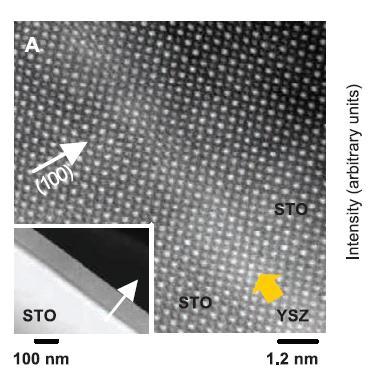

3 Motivation YSZ STO 10 nm STO
4 Surprising...but enormous potential if a real effect! Temperature ( C) Bi 2 O multilayer SDC/CeO 2 1nm YSZ log σ (Scm -1 ) YSZ/Y 2 O 3, Korte et al PCCP (2008) 10, GDZ/GDC on Al 2 O 3, Wang et al SSI (2006) 177, 1299 SDC/CeO 2 on MgO, Kosacki unpublished YSZ/STO, Garcia-Barriocanal et al Science (2008) 321, 676 thin film YSZ -12 YSZ thin films on MgO/Al 2 O 3, Karthikeyan et al APL (2006) 89, 183 YSZ thin films on MgO, Kosacki et al SSI (2005) 176, /T (K -1 ) Slide courtesy of John Kilner
5 PLD grown : SrTiO3 YSZ SrTiO3 multilayer Extensive mixing initially (consistent with in-situ RHEED). Change to layer-by-layer after 3 repeats (RHEED) A. Cavallaro et al. Solid State Ionics 181 (2010)
6 PLD : SrTiO3 YSZ SrTiO3 multilayer Coherent or semi-coherent chains Incoherent islands A. Cavallaro et al. Solid State Ionics 181 (2010)
7 PLD : EELS analysis the limits A. Cavallaro et al. Solid State Ionics 181 (2010)


8 EDX hyperspectral mapping HAADF O Sr Ti [110] SrTiO3

 0.002 0.001 0.000 2.93 1.")
9 Care : There are non-local effects in spectroscopic imaging Split signal into elastically scattered electrons and thermally diffused electrons EDX map for oxygen K-edge in SrTiO 3 [001]: Absorptive Model O Ti/O Sr Ti/O Fractional intensity Fractional intensity Probe position (Å) Probe position (Å) Probe position (Å) Probe position (Å) Elastic signal Thermal signal Born-Oppenheimer Contribution of thermally scattered electrons to atomic resolution elemental maps. Forbes, McComb, Allen et al, Phys Rev B 86 (2012)
10 Oxygen and Titanium Signals Collected from Ti/O O Ti/O Columns 300 kv α = 24 mrad β = 39 mrad t/λ =.19λ

11 Quantification : entire multilayer C A C B = k AB I A I B Fit background remove Bremsstrahlung Fit peaks overlap issues Integrate to obtain net counts Quantify Cliff Lorimer k-factor
12 Why calculated k-factors are dangerous! A : atomic weight Q : ionization cross-section ρ : density µ : linear absorption coeff. a : relative transition probability t : thickness ω : fluorescence yield ε : detector effciency Calculated values much have higher errors than the experimental data.
13 Determine Experimental k-factors Bulk SrTiO 3 wafer/substrate Bulk Y 2 O 3 -ZrO 2 crystal : composition established by SEM- EDX with elemental standards and Laser Ablation Inductively Coupled Plasma Mass Spectrometry (LA-ICP-MS) C A C B = k AB I A I B


14 Coherent layers in RF sputtered STO-YSZ-STO Samples grown & provided by J Santamaria et al


15 RF sputtered STO-YSZ-STO HAADF Sr Zr Ti Four 1nm layers of YSZ EDX shows that substrate STO buffer interface is Sr-rich YSZ layers appear to be continuous Samples grown & provided by J Santamaria et al Y


16 EDX mapping of RF sputtered STO-YSZ-STO PLD Sr Ti Zr Y

17 Quant 1 : RF sputtered STO-YSZ-STO Entire Layer : 13.6 mol% Y 2 O 3
 pixels i.e. each box is 0.")
18 Quantification 2 : RF sputtered STO-YSZ-STO Divide sample into 10 sub-regions Sub-regions are (256 x 4) pixels i.e. each box is 0.4nm in height Quantify each box for Sr, Ti, Y & Zr
19 Part I : Conclusions, comments & caveats Samples grown by BOTH PLD and RF sputtering show Y/Zr rich layers that are coherent with STO Sr & Ti present throughout the layer Ti concentration is more reduced than Sr in the Zrlayer Averaged composition of layers is higher than nominal target values Lower STO-YSZ interface is smoother/flatter than upper YSZ-STO interface

20 Computational study of structures of Y 2 O 3 - stabilised ZrO 2 /SrTiO 3 multilayers Wei Li Cheah, Mike W. Finnis, David W. McComb Department of Materials, Imperial College London, UK


")


21 Chua et al, A genetic algorithm for predicting the structures of interfaces in multicomponent systems., Nat Mater, 9 (2010) 418 Genetic algorithm Crossover Initial configuration New generation The genetic algorithm Mutation Tournament selection Exchange
22 YSZ/STO supercell Initial configuration for the genetic algorithm STO z ZrO 2 with 2 Zr 4+ replaced with Y 3+ and one O 2- removed Supercell with SrO-terminated STO interfaces STO O Zr Ti Sr
23 Result from the genetic algorithm and CASTEP O Zr Ti Sr Y Fluorite YSZ structure unstable Spontaneously transforms into a different structure Low energy structure from genetic algorithm confirmed with energy calculations within CASTEP This structure only with excess SrO? What about stoichiometric STO/excess TiO 2?
24 Result from the genetic algorithm and CASTEP O Zr Ti Sr Y Intermixing of YSZ and STO: Y 3+ in Sr 2+ lattice site Sr 2+ in Zr 4+ lattice site Zr 4+ in Ti 4+ lattice site Ti 4+ in Zr 4+ lattice site Cheah WL, Finnis MW, Structure of multilayer ZrO2/SrTiO3, J. Mat Sci, 47 (2012) 1631
25 Conclusion O Zr Ti Sr Y The lowest energy YSZ structure in a YSZ/STO multilayer, determined using a combination of classical and first principles-based methods, is different from the expected fluorite lattice and appears to favour interdiffusion. Cheah WL, Finnis MW, Structure of multilayer ZrO2/SrTiO3, J. Mat Sci, 47 (2012) 1631
26 Conclusions & Comments EDX spectrum imaging is easier to quantify that EELS mapping. Quantification on the sub-nanometre scale achievable provided due care is given to determination of experimental k-factors (or z-factors) and channelling effects. Atomic scale chemical maps provide qualitative insights but. Quantification on the atomic scale requires simulation of the images/maps due to non-local contributions in both EELS & EDX How do we relate the role of compositional fluctuations on ionic conductivity properties.
27 Thanks to Ohio Research Scholar Award (ODOD Third Frontier program) A*STAR programme (Wei Li Cheah) UK Engineering and Physical Sciences Research Council (EPSRC)
Atomic Resolution Interfacial Structure of Lead-free Ferroelectric
 Atomic Resolution Interfacial Structure of Lead-free Ferroelectric K 0.5 Na 0.5 NbO 3 Thin films Deposited on SrTiO 3 Chao Li 1, Lingyan Wang 1*, Zhao Wang 2, Yaodong Yang 2, Wei Ren 1 and Guang Yang 1
Segregated chemistry and structure on (001) and (100) surfaces of
 and (100) surfaces of") Supporting Information Segregated chemistry and structure on (001) and (100) surfaces of (La 1-x Sr x ) 2 CoO 4 override the crystal anisotropy in oxygen exchange kinetics Yan Chen a, Helena Téllez b,c,
Supporting Information Segregated chemistry and structure on (001) and (100) surfaces of (La 1-x Sr x ) 2 CoO 4 override the crystal anisotropy in oxygen exchange kinetics Yan Chen a, Helena Téllez b,c,
EELS Electron Energy Loss Spectroscopy
 EELS Electron Energy Loss Spectroscopy (Thanks to Steve Pennycook, Quan Li, Charlie Lyman, Ondre Krivenak, David Muller, David Bell, Natasha Erdman, Nestor Zaluzec and many others) Nestor Zaluzec,
Origin of the 2DEG at the LAO/STO Interface
 Origin of the 2DEG at the LAO/STO Interface Umberto Scotti di Uccio S. Amoruso, C. Aruta, R. Bruzzese, E. Di Gennaro, A. Sambri, X. Wang and F. Miletto Granozio University FEDERICO II & CNRSPIN, Napoli
in this web service Cambridge University Press
 High-k Materials Mat. Res. Soc. Symp. Proc. Vol. 670 2001 Materials Research Society Materials and Physical Properties of Novel High-k and Medium-k Gate Dielectrics Ran Liu, Stefan Zollner, Peter Fejes,
Depth profile study of ferroelectric PbZr 0.2 Ti 0.8 O 3 films
 JOURNAL OF APPLIED PHYSICS VOLUME 92, NUMBER 11 1 DECEMBER 2002 Depth profile study of ferroelectric PbZr 0.2 Ti 0.8 O 3 films Y. Li, V. Nagarajan, S. Aggarwal, R. Ramesh, L. G. Salamanca-Riba, and L.
A new era in surface diffraction pulsed laser deposition of complex metal oxide thin films
 A new era in surface diffraction pulsed laser deposition of complex metal oxide thin films Phil Willmott, Christian Schlepütz tz,, Roger Herger, Oliver Bunk, and Bruce Patterson Beamline X04SA Materials
Chemical Analysis in TEM: XEDS, EELS and EFTEM. HRTEM PhD course Lecture 5
 Chemical Analysis in TEM: XEDS, EELS and EFTEM HRTEM PhD course Lecture 5 1 Part IV Subject Chapter Prio x-ray spectrometry 32 1 Spectra and mapping 33 2 Qualitative XEDS 34 1 Quantitative XEDS 35.1-35.4
Elastic and Inelastic Scattering in Electron Diffraction and Imaging
 Elastic and Inelastic Scattering in Electron Diffraction and Imaging Contents Introduction Symbols and definitions Part A Diffraction and imaging of elastically scattered electrons Chapter 1. Basic kinematical
Aberration-corrected TEM studies on interface of multilayered-perovskite systems
 Aberration-corrected TEM studies on interface of multilayered-perovskite systems By Lina Gunawan (0326114) Supervisor: Dr. Gianluigi Botton November 1, 2006 MSE 702(1) Presentation Outline Literature Review
Techniques EDX, EELS et HAADF en TEM: possibilités d analyse et applications
 Techniques EDX, EELS et HAADF en TEM: possibilités d analyse et applications Thomas Neisius Université Paul Cézanne Plan Imaging modes HAADF Example: supported Pt nanoparticles Electron sample interaction
Strain-induced single-domain growth of epitaxial SrRuO 3 layers on SrTiO 3 : a high-temperature x-ray diffraction study
 Strain-induced single-domain growth of epitaxial SrRuO 3 layers on SrTiO 3 : a high-temperature x-ray diffraction study Arturas Vailionis 1, Wolter Siemons 1,2, Gertjan Koster 1 1 Geballe Laboratory for
Thin Film Bi-based Perovskites for High Energy Density Capacitor Applications
 ..SKELETON.. Thin Film Bi-based Perovskites for High Energy Density Capacitor Applications Colin Shear Advisor: Dr. Brady Gibbons 2010 Table of Contents Chapter 1 Introduction... 1 1.1 Motivation and Objective...
Electron Microscopy I
 Characterization of Catalysts and Surfaces Characterization Techniques in Heterogeneous Catalysis Electron Microscopy I Introduction Properties of electrons Electron-matter interactions and their applications
La superficie di film e cristalli di SrTiO 3
 U. Scotti di Uccio La superficie di film e cristalli di SrTiO 3 Coherentia-CNR-INFM Napoli, Italy Prof. R. Vaglio F. Miletto Granozio, N. Lampis, P. Perna, M. Radovic, A. Sambri M. Salluzzo, G. De Luca,
Electron Rutherford Backscattering, a versatile tool for the study of thin films
 Electron Rutherford Backscattering, a versatile tool for the study of thin films Maarten Vos Research School of Physics and Engineering Australian National University Canberra Australia Acknowledgements:
A constant potential of 0.4 V was maintained between electrodes 5 and 6 (the electrode
 (a) (b) Supplementary Figure 1 The effect of changing po 2 on the field-enhanced conductance A constant potential of 0.4 V was maintained between electrodes 5 and 6 (the electrode configuration is shown
TMT4320 Nanomaterials November 10 th, Thin films by physical/chemical methods (From chapter 24 and 25)
") 1 TMT4320 Nanomaterials November 10 th, 2015 Thin films by physical/chemical methods (From chapter 24 and 25) 2 Thin films by physical/chemical methods Vapor-phase growth (compared to liquid-phase growth)
1 TMT4320 Nanomaterials November 10 th, 2015 Thin films by physical/chemical methods (From chapter 24 and 25) 2 Thin films by physical/chemical methods Vapor-phase growth (compared to liquid-phase growth)
Laser matter interaction
 Laser matter interaction PH413 Lasers & Photonics Lecture 26 Why study laser matter interaction? Fundamental physics Chemical analysis Material processing Biomedical applications Deposition of novel structures
Deposited on: 19 January 2009
 Harkins, P. and MacKenzie, M. and Craven, A.J. and McComb, D.W. (2008) Quantitative electron energy-loss spectroscopy (EELS) analyses of lead zirconate titanate. Micron, 39 (6). pp. 709-716. ISSN 0968-4328.
Fundamentals of Nanoscale Film Analysis
 Fundamentals of Nanoscale Film Analysis Terry L. Alford Arizona State University Tempe, AZ, USA Leonard C. Feldman Vanderbilt University Nashville, TN, USA James W. Mayer Arizona State University Tempe,
MSE 321 Structural Characterization
 Auger Spectroscopy Auger Electron Spectroscopy (AES) Scanning Auger Microscopy (SAM) Incident Electron Ejected Electron Auger Electron Initial State Intermediate State Final State Physical Electronics
Nanoplasmonics: Classical down to the Nanometer Scale
 Supporting Information Nanoplasmonics: Classical down to the Nanometer Scale Huigao Duan #, Antonio I. Fernández-Domínguez 2#, Michel Bosman #, Stefan A. Maier 2* & Joel K. W. Yang * Institute of Materials
Patrick E. Hopkins Assistant Professor Dept. Mech. & Aero. Eng.
 Stephen R. Lee, Doug Medlin, Harlan Brown- Shaklee, Jon F. Ihlefeld Sandia NaConal Labs Strain field and coherent domain wall effects on the thermal conducevity and Kapitza conductance in Bismuth Ferrite
L YBCO è di MODA! U. Scotti di Uccio
 L YBCO è di MODA! U. Scotti di Uccio Coherentia-CNR-INFM Napoli, Italy Prof. R. Vaglio F. Miletto Granozio, M. Radovic, N. Lampis, P. Perna, A. Sambri M. Salluzzo, G. De Luca, R. Di Capua, A. Gambardella,
Transmission Electron Microscopy for metrology and characterization of semiconductor devices
 Transmission Electron Microscopy for metrology and characterization of semiconductor devices Bert Freitag, Laurens Kwakman, Ivan Lazic and Frank de Jong FEI / ThermoFisher Scientific, Achtseweg Noord 5,
arxiv: v1 [cond-mat.mtrl-sci] 9 Apr 2007
![arxiv: v1 [cond-mat.mtrl-sci] 9 Apr 2007](/thumbs/93/118034102.jpg "arxiv: v1 [cond-mat.mtrl-sci] 9 Apr 2007") Electrical transport properties of polar heterointerface between KTaO 3 and SrTiO 3 A. Kalabukhov, 1, R. Gunnarsson, 1 T. Claeson, 1 and D. Winkler 1 arxiv:0704.1050v1 [cond-mat.mtrl-sci] 9 Apr 2007 1
Electrical transport properties of polar heterointerface between KTaO 3 and SrTiO 3 A. Kalabukhov, 1, R. Gunnarsson, 1 T. Claeson, 1 and D. Winkler 1 arxiv:0704.1050v1 [cond-mat.mtrl-sci] 9 Apr 2007 1
Temperature dependence of microwave and THz dielectric response
 The 10 th European Meeting on Ferroelectricity, August 2003, Cambridge, UK Ferroelectrics, in press. Temperature dependence of microwave and THz dielectric response in Sr n+1 Ti n O 3n+1 (n=1-4) D. Noujni
MT Electron microscopy Scanning electron microscopy and electron probe microanalysis
 MT-0.6026 Electron microscopy Scanning electron microscopy and electron probe microanalysis Eero Haimi Research Manager Outline 1. Introduction Basics of scanning electron microscopy (SEM) and electron
Electronic Properties of Lead Telluride Quantum Wells
 Electronic Properties of Lead Telluride Quantum Wells Liza Mulder Smith College 2013 NSF/REU Program Physics Department, University of Notre Dame Advisors: Profs. Jacek Furdyna, Malgorzata Dobrowolska,
Study of interface asymmetry in InAs GaSb heterojunctions
 Study of interface asymmetry in InAs GaSb heterojunctions M. W. Wang, D. A. Collins, and T. C. McGill T. J. Watson, Sr. Laboratory of Applied Physics, California Institute of Technology, Pasadena, California
Supplementary Information
 Supplementary Information Direct observation of crystal defects in an organic molecular crystals of copper hexachlorophthalocyanine by STEM-EELS Mitsutaka Haruta*, Hiroki Kurata Institute for hemical Research,
X-ray diffraction and Crystal Structure Solutions from Thin Films
 X-ray diffraction and Crystal Structure Solutions from Thin Films Ingo Salzmann Humboldt-Universität zu Berlin Institut für Physik Overview Experimental technique X-ray diffraction The principal phenomenon
Supplementary Figure 1 Comparison between normalized and unnormalized reflectivity of
 Supplementary Figures Supplementary Figure 1 Comparison between normalized and unnormalized reflectivity of bulk SrTiO 3. The normalized high-energy reflectivity (0.5 35 ev) of SrTiO 3 is compared to the
Steady-state diffusion is diffusion in which the concentration of the diffusing atoms at
 Chapter 7 What is steady state diffusion? Steady-state diffusion is diffusion in which the concentration of the diffusing atoms at any point, x, and hence the concentration gradient at x, in the solid,
CHEM-E5225 :Electron Microscopy X-Ray Spectrometry
 CHEM-E5225 :Electron Microscopy X-Ray Spectrometry 2016.11 Yanling Ge Outline X-ray Spectrometry X-ray Spectra and Images Qualitative and Quantitative X-ray Analysis and Imaging Discussion of homework
Magnetoresistance of 2D and 3D Electron Gas in LaAlO 3 /SrTiO 3. Heterostructures: Influence of Magnetic Ordering, Interface Scattering and
 Magnetoresistance of 2D and 3D Electron Gas in LaAlO 3 /SrTiO 3 Heterostructures: Influence of Magnetic Ordering, Interface Scattering and Dimensionality X. Wang 1,2, W.M Lü 1,2, A. Annadi 1,2, Z.Q. Liu
Secondary Ion Mass Spectrometry (SIMS)
") CHEM53200: Lecture 10 Secondary Ion Mass Spectrometry (SIMS) Major reference: Surface Analysis Edited by J. C. Vickerman (1997). 1 Primary particles may be: Secondary particles can be e s, neutral species
CHEM53200: Lecture 10 Secondary Ion Mass Spectrometry (SIMS) Major reference: Surface Analysis Edited by J. C. Vickerman (1997). 1 Primary particles may be: Secondary particles can be e s, neutral species
6. Analytical Electron Microscopy
 Physical Principles of Electron Microscopy 6. Analytical Electron Microscopy Ray Egerton University of Alberta and National Institute of Nanotechnology Edmonton, Canada www.tem-eels.ca regerton@ualberta.ca
Modeling the sputter deposition of thin film photovoltaics using long time scale dynamics techniques
 Loughborough University Institutional Repository Modeling the sputter deposition of thin film photovoltaics using long time scale dynamics techniques This item was submitted to Loughborough University's
Electrostatic Modification of Cuprates. Allen M. Goldman School of Physics and Astronomy University of Minnesota
 Electrostatic Modification of Cuprates Allen M. Goldman School of Physics and Astronomy University of Minnesota Principal Collaborators Xiang Leng (BNL) Javier Garcia-Barriocanal (Complutense) Joseph Kinney
Room-temperature tunable microwave properties of strained SrTiO 3 films
 JOURNAL OF APPLIED PHYSICS VOLUME 96, NUMBER 11 1 DECEMBER 2004 Room-temperature tunable microwave properties of ed SrTiO 3 films Wontae Chang, a) Steven W. Kirchoefer, Jeffrey M. Pond, Jeffrey A. Bellotti,
MT Electron microscopy Scanning electron microscopy and electron probe microanalysis
 MT-0.6026 Electron microscopy Scanning electron microscopy and electron probe microanalysis Eero Haimi Research Manager Outline 1. Introduction Basics of scanning electron microscopy (SEM) and electron
What so special about LaAlO3/SrTiO3 interface? Magnetism, Superconductivity and their coexistence at the interface
 What so special about LaAlO3/SrTiO3 interface? Magnetism, Superconductivity and their coexistence at the interface Pramod Verma Indian Institute of Science, Bangalore 560012 July 24, 2014 Pramod Verma
SIMULATION OF TRANSMISSION AND SCANNING TRANSMISSION ELECTRON MICROSCOPIC IMAGES CONSIDERING ELASTIC AND THERMAL DIFFUSE SCATTERING
 Scanning Microscopy Vol. 11, 1997 (Pages 277-286) 0891-7035/97$5.00+.25 Scanning Microscopy International, Chicago (AMF Simulation O Hare), of TEM IL 60666 and STEM USA images SIMULATION OF TRANSMISSION
Structure analysis: Electron diffraction LEED TEM RHEED
 Structure analysis: Electron diffraction LEED: Low Energy Electron Diffraction SPA-LEED: Spot Profile Analysis Low Energy Electron diffraction RHEED: Reflection High Energy Electron Diffraction TEM: Transmission
Analytical Electron Microscopy
 Analytical Electron Microscopy Walid Hetaba Fritz-Haber-Institut der MPG MPI für Chemische Energiekonversion hetaba@fhi-berlin.mpg.de 10.11.2017 W. Hetaba (FHI, MPI-CEC) Analytical Electron Microscopy
Electrostatic charging and redox effects in oxide heterostructures
 Electrostatic charging and redox effects in oxide heterostructures Peter Littlewood 1,2,3 Nick Bristowe 3 & Emilio Artacho 3,6 Miguel Pruneda 4 and Massimiliano Stengel 5 1 Argonne National Laboratory
In-situ Multilayer Film Growth Characterization by Brewster Angle Reflectance Differential Spectroscopy
 In-situ Multilayer Film Growth Characterization by Brewster Angle Reflectance Differential Spectroscopy N. Dietz, D.J. Stephens, G. Lucovsky and K.J. Bachmann North Carolina State University, Raleigh,
In situ growth of nanoparticles through control of non-stoichiometry
 DOI: 10.1038/NCHEM.1773 In situ growth of nanoparticles through control of non-stoichiometry Dragos Neagu 1 *, George Tsekouras 1, David N. Miller 1, Hervé Ménard 2 and John T.S. Irvine 1 * 1 University
arxiv: v1 [cond-mat.mtrl-sci] 19 Oct 2011
![arxiv: v1 [cond-mat.mtrl-sci] 19 Oct 2011](/thumbs/94/119431574.jpg "arxiv: v1 [cond-mat.mtrl-sci] 19 Oct 2011") Pulsed laser deposition growth of heteroepitaxial YBa 2 Cu 3 O 7 /La 0.67 Ca 0.33 MnO 3 superlattices on NdGaO 3 and Sr 0.7 La 0.3 Al 0.65 Ta 0.35 O 3 substrates arxiv:1110.4173v1 [cond-mat.mtrl-sci] 19
Pulsed laser deposition growth of heteroepitaxial YBa 2 Cu 3 O 7 /La 0.67 Ca 0.33 MnO 3 superlattices on NdGaO 3 and Sr 0.7 La 0.3 Al 0.65 Ta 0.35 O 3 substrates arxiv:1110.4173v1 [cond-mat.mtrl-sci] 19
FIRST-PRINCIPLES MODELING OF OXYGEN INTERACTION WITH ABO 3 -TYPE PEROVSKITE SURFACES
 FIRST-PRINCIPLES MODELING OF OXYGEN INTERACTION WITH ABO 3 -TYPE PEROVSKITE SURFACES S. Piskunov, E.A. Kotomin, Yu.F. Zhukovskii, and V. Alexandrov FMNT 2010, Riga, March 17 Motivation: Oxygen adsorption
Ferroelectrics. Spartak Gevorgian. Department of Microtechnology and Nanoscience Chalmers University of Technology Gothenburg, Sweden
 Ferroelectrics Material Properties, Processing, and Microwave Applications Spartak Gevorgian Department of Microtechnology and Nanoscience Chalmers University of Technology Gothenburg, Sweden Norwegian
SUPPLEMENTARY INFORMATION
 In the format provided by the authors and unedited. DOI: 10.1038/NMAT4879 Real time impedance monitoring of oxygen reduction during surface modification of thin film cathodes Ghislain M. Rupp 1,*, Alexander
Pulsed laser deposition of PZT and PLZT
 Chapter 3 Pulsed laser deposition of PZT and PLZT A lower growth temperature of PZT films is favored for integration of these films for MEMS application. This chapter gives a detailed account of the work
Electron energy loss spectroscopy (EELS)
") Electron energy loss spectroscopy (EELS) Phil Hasnip Condensed Matter Dynamics Group Department of Physics, University of York, U.K. http://www-users.york.ac.uk/~pjh503 Many slides courtesy of Jonathan
Electron energy loss spectroscopy (EELS) Phil Hasnip Condensed Matter Dynamics Group Department of Physics, University of York, U.K. http://www-users.york.ac.uk/~pjh503 Many slides courtesy of Jonathan
Effects of plasma treatment on the precipitation of fluorine-doped silicon oxide
 ARTICLE IN PRESS Journal of Physics and Chemistry of Solids 69 (2008) 555 560 www.elsevier.com/locate/jpcs Effects of plasma treatment on the precipitation of fluorine-doped silicon oxide Jun Wu a,, Ying-Lang
CHEM*3440. Photon Energy Units. Spectrum of Electromagnetic Radiation. Chemical Instrumentation. Spectroscopic Experimental Concept.
 Spectrum of Electromagnetic Radiation Electromagnetic radiation is light. Different energy light interacts with different motions in molecules. CHEM*344 Chemical Instrumentation Topic 7 Spectrometry Radiofrequency
Newcastle University eprints
 Newcastle University eprints Ponon NK, Appleby DJR, Arac E, Kwa KSK, Goss JP, Hannemann U, Petrov PK, Alford NM, O'Neill A. Impact of Crystalline Orientation on the Switching Field in Barium Titanate Using
Abstract Using polarized neutron reflectometry (PNR) we measured the neutron spin
 we measured the neutron spin") Upper limit to magnetism in LaAlO 3 /SrTiO 3 heterostructures M. R. Fitzsimmons, 1 N. Hengartner, 1 S. Singh, 1,2 M. Zhernenkov, 1 F. Y. Bruno 3, J. Santamaria, 3 A. Brinkman, 4 M. Huijben, 4 H. Molegraaf,
Upper limit to magnetism in LaAlO 3 /SrTiO 3 heterostructures M. R. Fitzsimmons, 1 N. Hengartner, 1 S. Singh, 1,2 M. Zhernenkov, 1 F. Y. Bruno 3, J. Santamaria, 3 A. Brinkman, 4 M. Huijben, 4 H. Molegraaf,
Opportunities for Advanced Plasma and Materials Research in National Security
 Opportunities for Advanced Plasma and Materials Research in National Security Prof. J.P. Allain allain@purdue.edu School of Nuclear Engineering Purdue University Outline: Plasma and Materials Research
When transition metals are incorporated into a certain site of the BiT, some of BiT-LaTMO 3
 Band gap tuning in ferroelectric Bi 4 Ti 3 O 12 by alloying LaTMO 3 (TM = Ti, V, Cr, Mn, Co, Ni, and Al) Woo Seok Choi and Ho Nyung Lee Materials Science and Technology Division, Oak Ridge National Laboratory,
Nanoscale voxel spectroscopy by simultaneous EELS and EDS tomography
 Electronic Supplementary Material (ESI) for Nanoscale. This journal is The Royal Society of Chemistry 2014 Supplementary Information Nanoscale voxel spectroscopy by simultaneous EELS and EDS tomography
SUPPLEMENTARY INFORMATION
 SUPPLEMENTARY INFORMATION Reversible Electric Control of Exchange Bias in a Multiferroic Field Effect Device S. M. Wu 1, 2, Shane A. Cybart 1, 2, P. Yu 1, 2, M. D. Abrodos 1, J. Zhang 1, R. Ramesh 1, 2
Sputter Ion Pump (Ion Pump) By Biswajit
 By Biswajit") Sputter Ion Pump (Ion Pump) By Biswajit 08-07-17 Sputter Ion Pump (Ion Pump) An ion pump is a type of vacuum pump capable of reaching pressures as low as 10 11 mbar under ideal conditions. An ion pump
Sputter Ion Pump (Ion Pump) By Biswajit 08-07-17 Sputter Ion Pump (Ion Pump) An ion pump is a type of vacuum pump capable of reaching pressures as low as 10 11 mbar under ideal conditions. An ion pump
High resolution ion beam analysis. Torgny Gustafsson
 High resolution ion beam analysis Torgny Gustafsson Review articles and Books L. C. Feldman, J. W. Mayer and S. T. Picraux, Materials Analysis by Ion Channeling, Academic Press (1982) I. Stensgaard, Surface
Supporting Information
 Supporting Information Extraordinary Off-stoichiometric Bismuth Telluride for Enhanced n- type Thermoelectric Power Factor Kunsu Park,,,# Kyunghan Ahn,,# Joonil Cha,, Sanghwa Lee,, Sue In Chae,, Sung-
Application of the GD-Profiler 2 to the PV domain
 Application of the GD-Profiler 2 to the PV domain GD Profiler 2 RF GDOES permits to follow the distribution of the elements as function of depth. This is an ultra fast characterisation technique capable
Module17: Intermolecular Force between Surfaces and Particles. Lecture 23: Intermolecular Force between Surfaces and Particles
 Module17: Intermolecular Force between Surfaces and Particles Lecture 23: Intermolecular Force between Surfaces and Particles 1 We now try to understand the nature of spontaneous instability in a confined
Mapping Atomic Structure at Epitaxial Interfaces
 Mapping Atomic Structure at Epitaxial Interfaces Roy Clarke, University of Michigan, Ann Arbor, MI Opportunities for interface science at the ERL royc@umich.edu ERL X-ray Science Workshop: Almost Impossible
Chris G. Van de Walle
 Complex oxide interfaces Chris G. Van de Walle Anderson Janotti, Lars Bjaalie, Luke Gordon, Burak Himmetoglu, K. Krishnaswamy Materials Department, University of California, Santa Barbara ES213 June 11-14,
Giant tunability of the two-dimensional electron gas at the interface of -Al 2 O 3 /SrTiO 3
 Supporting Information Giant tunability of the two-dimensional electron gas at the interface of -Al 2 O 3 /SrTiO 3 Wei Niu,, Yu Zhang, Yulin Gan, Dennis V. Christensen, Merlin V. Soosten, Eduardo J. Garcia-Suarez,
Polar Discontinuity Doping of the LaVO 3 /SrTiO 3 Interface
 Polar Discontinuity Doping of the LaVO 3 /SrTiO 3 Interface Y. Hotta, 1,a T. Susaki, 1 and H. Y. Hwang 1,2,b 1 Department of Advanced Materials Science, University of Tokyo, Kashiwa, Chiba 277-8651, Japan
DEPOSITION OF THIN TiO 2 FILMS BY DC MAGNETRON SPUTTERING METHOD
 Chapter 4 DEPOSITION OF THIN TiO 2 FILMS BY DC MAGNETRON SPUTTERING METHOD 4.1 INTRODUCTION Sputter deposition process is another old technique being used in modern semiconductor industries. Sputtering
Electronic Structure and Band Alignment of LaMnO 3 /SrTiO 3 Polar/Nonpolar Heterojunctions
 FULL PAPER Polar/Non-Polar Heterojunctions Electronic Structure and Band Alignment of LaMnO 3 /SrTiO 3 Polar/Nonpolar Heterojunctions Tiffany C. Kaspar,* Peter V. Sushko, Steven R. Spurgeon, Mark E. Bowden,
Nanoscale magnetic imaging with single spins in diamond
 Nanoscale magnetic imaging with single spins in diamond Ania Bleszynski Jayich UC Santa Barbara Physics AFOSR Nanoelectronics Review Oct 24, 2016 Single spin scanning magnetometer Variable temperature
From Nanoparticles to Single Atoms, EDS of Electron Transparent Samples. M. Falke, et al.
 From Nanoparticles to Single Atoms, EDS of Electron Transparent Samples M. Falke, et al. 1 Presenters Dr. Meiken Falke Product Manager EDS/TEM, Bruker Nano Analytics, Berlin, Germany Dr. Igor Nemeth Application
In situ optical characterization of LaAlO 3 epitaxy on SrTiO 3 (001)
") February 2015 EPL, 109 (2015) 37006 doi: 10.1209/0295-5075/109/37006 www.epljournal.org In situ optical characterization of LaAlO 3 epitaxy on SrTiO 3 (001) X. D. Zhu 1(a), Sebastian Wicklein 2, Felix
February 2015 EPL, 109 (2015) 37006 doi: 10.1209/0295-5075/109/37006 www.epljournal.org In situ optical characterization of LaAlO 3 epitaxy on SrTiO 3 (001) X. D. Zhu 1(a), Sebastian Wicklein 2, Felix
Acidic Water Monolayer on Ruthenium(0001)
") Acidic Water Monolayer on Ruthenium(0001) Youngsoon Kim, Eui-seong Moon, Sunghwan Shin, and Heon Kang Department of Chemistry, Seoul National University, 1 Gwanak-ro, Seoul 151-747, Republic of Korea.
Acidic Water Monolayer on Ruthenium(0001) Youngsoon Kim, Eui-seong Moon, Sunghwan Shin, and Heon Kang Department of Chemistry, Seoul National University, 1 Gwanak-ro, Seoul 151-747, Republic of Korea.
Nitrogen-Vacancy Centers in Diamond A solid-state defect with applications from nanoscale-mri to quantum computing
 Nitrogen-Vacancy Centers in Diamond A solid-state defect with applications from nanoscale-mri to quantum computing Research into nitrogen-vacancy centers in diamond has exploded in the last decade (see
PHYS-E0541:Special Course in Physics Gas phase synthesis of carbon nanotubes for thin film application. Electron Microscopy. for
 PHYS-E0541:Special Course in Physics Gas phase synthesis of carbon nanotubes for thin film application Electron Microscopy for Introduction to Electron Microscopy Carbon Nanomaterials (nanotubes) Dr. Hua
Solid State Science and Technology, Vol. 13, No 1 & 2 (2005) ISSN
 ISSN") FABRICATION OF Bi-Ti-O THIN FILM PRESSURE SENSOR PREPARED BY ELECTRON BEAM EVAPORATION METHOD Chong Cheong Wei, Muhammad Yahaya and Muhamad Mat Salleh Institue of Microengineering and Nanoelectronics,
FABRICATION OF Bi-Ti-O THIN FILM PRESSURE SENSOR PREPARED BY ELECTRON BEAM EVAPORATION METHOD Chong Cheong Wei, Muhammad Yahaya and Muhamad Mat Salleh Institue of Microengineering and Nanoelectronics,
Supporting Information
 Electronic Supplementary Material (ESI) for Journal of Materials Chemistry A. This journal is The Royal Society of Chemistry 2014 Supporting Information Sustainable photocatalytic production of hydrogen
EE 527 MICROFABRICATION. Lecture 5 Tai-Chang Chen University of Washington
 EE 527 MICROFABRICATION Lecture 5 Tai-Chang Chen University of Washington MICROSCOPY AND VISUALIZATION Electron microscope, transmission electron microscope Resolution: atomic imaging Use: lattice spacing.
Electrical Conduction in Ceramic Materials 1 Ref: Barsoum, Fundamentals of Ceramics, Ch7, McGraw-Hill, 2000
 MME 467 Ceramics for Advanced Applications Lecture 19 Electrical Conduction in Ceramic Materials 1 Ref: Barsoum, Fundamentals of Ceramics, Ch7, McGraw-Hill, 2000 Prof. A. K. M. B. Rashid Department of
IMAGING DIFFRACTION SPECTROSCOPY
 TEM Techniques TEM/STEM IMAGING DIFFRACTION SPECTROSCOPY Amplitude contrast (diffracion contrast) Phase contrast (highresolution imaging) Selected area diffraction Energy dispersive X-ray spectroscopy
GeSi Quantum Dot Superlattices
 GeSi Quantum Dot Superlattices ECE440 Nanoelectronics Zheng Yang Department of Electrical & Computer Engineering University of Illinois at Chicago Nanostructures & Dimensionality Bulk Quantum Walls Quantum
Overview of scattering, diffraction & imaging in the TEM
 Overview of scattering, diffraction & imaging in the TEM Eric A. Stach Purdue University Scattering Electrons, photons, neutrons Radiation Elastic Mean Free Path (Å)( Absorption Length (Å)( Minimum Probe
Auger Electron Spectroscopy
 Auger Electron Spectroscopy Auger Electron Spectroscopy is an analytical technique that provides compositional information on the top few monolayers of material. Detect all elements above He Detection
Characterisation of Nanoparticle Structure by High Resolution Electron Microscopy
 Journal of Physics: Conference Series OPEN ACCESS Characterisation of Nanoparticle Structure by High Resolution Electron Microscopy To cite this article: Robert D Boyd et al 2014 J. Phys.: Conf. Ser. 522
Spontaneous lateral composition modulation in InAlAs and InGaAs short-period superlattices
 Physica E 2 (1998) 325 329 Spontaneous lateral composition modulation in InAlAs and InGaAs short-period superlattices D.M. Follstaedt *, R.D. Twesten, J. Mirecki Millunchick, S.R. Lee, E.D. Jones, S.P.
Contents. Bibliografische Informationen digitalisiert durch
 1 Simulation of the Sputtering Process T. Ono, T. Kenmotsu, and T. Muramoto 1 1.1 Introduction 1 1.2 Computer Simulation Codes 2 1.3 Total Sputtering Yield 5 1.3.1 Incident-Energy Dependence of Sputtering
Applications of XPS, AES, and TOF-SIMS
 Applications of XPS, AES, and TOF-SIMS Scott R. Bryan Physical Electronics 1 Materials Characterization Techniques Microscopy Optical Microscope SEM TEM STM SPM AFM Spectroscopy Energy Dispersive X-ray
X-rays. X-ray Radiography - absorption is a function of Z and density. X-ray crystallography. X-ray spectrometry
 X-rays Wilhelm K. Roentgen (1845-1923) NP in Physics 1901 X-ray Radiography - absorption is a function of Z and density X-ray crystallography X-ray spectrometry X-rays Cu K α E = 8.05 kev λ = 1.541 Å Interaction
Harvesting Heat through Seebeck Spin Tunneling Effect
 Harvesting Heat through Seebeck Spin Tunneling Effect Costel Constantin James Madison University Science Enabled by Photon Source, May 2012 Outline 1. Spintronics vs. Spin Caloritronics. 2. Novel Spin
Plasma-Surface Interactions in Patterning High-k k Dielectric Materials
 Plasma-Surface Interactions in Patterning High-k k Dielectric Materials October 11, 4 Feature Level Compensation and Control Seminar Jane P. Chang Department of Chemical Engineering University of California,
Characterisation of vibrational modes of adsorbed species
 17.7.5 Characterisation of vibrational modes of adsorbed species Infrared spectroscopy (IR) See Ch.10. Infrared vibrational spectra originate in transitions between discrete vibrational energy levels of
Ordered Peierls distortion prevented at growth. onset of GeTe ultra-thin films
 Ordered Peierls distortion prevented at growth onset of GeTe ultra-thin films Ruining Wang 1, Davide Campi 2, Marco Bernasconi 2, Jamo Momand 3, Bart J. Kooi 3, Marcel A. Verheijen, 4 Matthias Wuttig,
Supplementary Figures:
 Supplementary Figures: Supplementary Figure 1 Cross-sectional morphology and Chemical composition. (a) A low-magnification dark-field TEM image shows the cross-sectional morphology of the BWO thin film