Auger Electron Spectrometry. EMSE-515 F. Ernst
|
|
|
- Cornelius Carson
- 5 years ago
- Views:
Transcription
1 Auger Electron Spectrometry EMSE-515 F. Ernst 1

2 Principle of AES electron or photon in, electron out radiation-less transition Auger electron electron energy properties of atom 2
 community came to attach Auger s name to it 1953 J.")
3 Brief History of Auger Electron Spectrometry 1923 discovered by Lise Meitner reported in Zeitschrift für Physik two years before Pierre Auger (?) but: English speaking scientific (?) community came to attach Auger s name to it 1953 J. J. Lander: idea of using electron-stimulated Auger signals for surface analysis 1967 Larry Harris: demonstrated use of spectrum di erentiation for enhancing the Auger signals today AES: very frequent analytical method for surfaces, thinfilms, and interface compositions 3


4 Brief History of Auger Electron Spectrometry Lise Meitner Pierre Auger 4

5 Basic Concept escape depth of Auger electrons: nm identification of elements via binding energies of electrons near the core energy of an Auger electron: di erence in binding energies between the vacant state the electron that fills the vacant state energy loss associated with reaching the surface 5
 L 1 L 2 M 1 Coster Kronig transition final state vacancy in the same shell as primary vacancy here: initial L 1 hole, filled with electron from the same shell (but di erent")
6 Examples of Two-Electron De-Exitation KL 1 L 1 Auger transition: initial K hole, filled with an L 1 electron simultaneously, the other L 1 electron is ejected LM 1 M 1 Auger transition: initial L hole (2s vacancy) L 1 L 2 M 1 Coster Kronig transition final state vacancy in the same shell as primary vacancy here: initial L 1 hole, filled with electron from the same shell (but di erent subshell) much higher rate than normal Auger transitions dominant (here: reducing M to L 1 vacancy transitions) 6

7 Examples of Two-Electron De-Exitation 7

8 Nomenclature three letters denoting the involved electron states the state of the initial vacancy the state of the electron that fills the vacancy the state of the electron being ejected Auger electron no dipole selection rules as for photon emission example: KLL transition initial vacancy on the K shell L electron fills the vacancy L electron is emitted subscripts denote subshells (e. g. KL 1 L 1, KL 1 L3, LM 1 M 1 ) 8
 example: Si KLL transition: KL 1 L 2,3 LVV transition: L 2,3 V 1 V 2 V 1 and V 2 located at local maxima of the density of states 9")
9 Nomenclature strongest transitions between electrons whose orbitals are closest together: KLL, LMM, Coster Kronig transitions vacancy is filled by electron from the same shell example: LLM Auger transitions involving the valence band (V) example: Si KLL transition: KL 1 L 2,3 LVV transition: L 2,3 V 1 V 2 V 1 and V 2 located at local maxima of the density of states 9


10 Auger Transitions Involving the Valence Band: Si 10
 2p shell occupied with 6 electrons final state: 2s 0")
11 Nomenclature even in simple KLL transition, there are a large variety of final states slightly di erent energies of the Auger electrons slightly di erent lines in the spectrum final state of the atom is usually described using spectroscopic notation example: KL 1 L 1 transition initial state: 1s hole final state: 2s shell empty (two vacancies) 2p shell occupied with 6 electrons final state: 2s 0 2p 6 11

12 Nomenclature example: KL 1 L 1 transition (continued) states correspond to the possible allowed quantum numbers consistent with Pauli principle: m s = 1, 0, +1; M L = 0; M s = 0 m s : magnetic quantum number, M L : total orbital angular momentum, M s : total spin angular momentum. total orbital momentum of zero denoted as 1 S ( 1 S is the only allowed final state, thus this notation is redundant) complete description: KL 1 L 1 2s 0 2p 6 ( 1 S) 12
 P: total orbital angular momentum L = 1. corresponds to two states coupling to total angular momentum L = 1 13")
13 Nomenclature example: KL 1 L 2 or KL 1 L3 transition initial state: 1s hole final state: one vacancy in 2s shell, one in 2p shell 2s shell occupied with 1 electron, 2p shell with 5 electrons final state: 2s 1 2p 5 possible quantum states: 1 P and 3 P (spins aligned or anti-aligned) P: total orbital angular momentum L = 1. corresponds to two states coupling to total angular momentum L = 1 13
14 Nomenclature example: KL 1 L 2 or KL 1 L3 transition (continued) a P state with the electron spins aligned: 3 P the electron spins anti-aligned: 1 P complete description: KL 1 L 2 2s 1 2p 5 ( 1 P), or KL 1 L 3 2s 1 2p 5 ( 3 P) 14
 P (L = 1) D (L = 2) KLL transitions yield six di erent final states: KL 1 L 1 2s 0 2p 6 ( 1 S) KL 1 L 2,3 2s 1 2p 5 ( 1 P, 3 P) KL 2,3 L 2,3 2s 2 2p 4 ( 1 D, 3 P, 1 S)")
15 Nomenclature example: KL 2 L 2, KL 2 L 3, or KL 3 L 3 transition initial state: 1s hole final state: two vacancies in 2 p shell 6 electrons remain in the L shell final states can couple to total angular momenti of S (L = 0) P (L = 1) D (L = 2) KLL transitions yield six di erent final states: KL 1 L 1 2s 0 2p 6 ( 1 S) KL 1 L 2,3 2s 1 2p 5 ( 1 P, 3 P) KL 2,3 L 2,3 2s 2 2p 4 ( 1 D, 3 P, 1 S) 15
 not observed small intensity")
16 Nomenclature spectrum showing six di erent states for Mg KL 2,3 L 2,3 2s 2 2p 4 ( 3 P) not observed small intensity 16

17 Energies energy of Auger electrons: consider di erence of the total energy before and after the transition empirical approach: E Z = EZ E Z E Z 1 2 EZ+1 E Z + EZ+1 E Z E Z : Auger energy of the transition of element Z. first three terms: di erence in binding energies of shells Z, Z, Z correction term (small): average of increase in binding energy of the -electron when a -electron is removed the -electron when a -electron is removed 17
: E Ni K = 8.333 ECu L 2 = 0.951 E Cu L 1 = 1.096 E Ni L 1 = 1.008 E Ni L 1 = 0.872 E Ni L 2 = 0.872 E Ni L 1 = 1.008 = 0.645 = 0.079 = 0.088 E Ni KL 1 L 2 = 6.543 kev 0.084 kev = 6.")
18 Numerical Example: KL 1 L 2 Auger Transition in Ni estimate for the energy of the Auger electron: EKL Ni 1 L = E Ni 2 K E Ni L 1 EL Ni ECu L 2 E Ni L 2 + E Cu L 1 EL Ni 1 electron binding energies (kev): E Ni K = ECu L 2 = E Cu L 1 = E Ni L 1 = E Ni L 1 = E Ni L 2 = E Ni L 1 = = = = E Ni KL 1 L 2 = kev kev = kev experimental value: kev good agreement 18

19 Auger Energies versus Atomic Number 19
20 Auger Energies versus Atomic Number heavy points indicate strong transitions binding energies depend strongly on Z Auger electron spectroscopy enables straight-forward identification of elements! 20

21 Chemical Shifts chemical environment of an atom changes in valence shell orbitals binding energy of core electrons binding energies of K and L shells shift in the same sense K X-ray emission energy does not vary significantly with chemical environment compare LL Auger transitions: K and L shells involved as in K X-ray emission however: L shell is involved twice KLL Auger electron energy will display chemical shift 21

22 Chemical Shifts AES: chemical shifts, similar to XPS however: chemical shifts in Auger spectra more di interpret cult to process involves two electrons compare: chemical shift in XPS spectra involves only one electron Auger spectra feature larger linewidths than XPS spectra less energy resolution XPS more suitable than AES to study chemical shifts 22
 transition: X = W X W A + W X = W X/W A 1 + W")
23 Yield of Auger Electrons and Fluorescence Yield lifetime of an excited state is detemined by probability W X for radiative transition (X-ray emission) probability W A for Auger transitions probability W K for Coster Kronig transitions consider transition to vacancy in the K shell no Coster Kronig transition probability for radiative (X-ray) transition: X = W X W A + W X = W X/W A 1 + W X /W A X : fluorescence yield. 23

24 Yield of Auger Electrons and Fluorescence Yield probability for radiative decay Z 4 Auger probability does not depend on Z semi-empirical relation: W X W A = a + bz cz 3 4 a = , b = , c =

25 Auger Electron Yield versus X-ray Yield per K Vacancy as a Function of the Atomic Number Z 25


26 Fluorescence Yield for K, L 3, and M5 Shells versus binding energy 26
 independent of the electronic shell (provided that Coster Kronig transitions do not occur)")
27 Apger Electron versus Fluorescence Yield fluorescence yield X is approximately the same for comparable transition energies X is (nearly) independent of the electronic shell (provided that Coster Kronig transitions do not occur) 27

28 Atomic Level Width and Lifetimes energy width is related to the mean lifetime of the excited state through Heisenberg s uncertainty principle decay probability per unit time equals the sum of the transition probabilities for radiative and non-radiative decay total energy width: = radiative + non-radiative each atomic process has its own probability however, there is only a single lifetime for the hole natural line width corresponds to total lifetime 28

29 Atomic Level Width and Lifetimes total width of atomic transition ev in the regime of dominant Auger emission (Z < 30) up to 30 ev for K X-ray emission in the regime of dominant X-ray emission (Z > 30) X-ray line broadening increases with Z Al or Mg sources for XPS 29
30 Auger Electron Spectroscopy AES ultra-high vacuum electron gun to generate focused electron beam electron energy analyzer 30

31 Principle of an Experimental Apparatus 31

32 Scanning Auger Microprobe PHI 680 System in CSAM field-emission gun scanning electron microscope UHV Schottky emitter secondary electron detector axial cylindrical mirror analyzer very small spot sizes 7 nm inert gas sputtering PHI ion gun remove surface contamination depth profiling 32

33 Scanning Auger Microprobe PHI 680 System in CSAM 33
 houses PHI 3600 secondary ion mass spectrometer")
34 Scanning Auger Microprobe PHI 680 System in CSAM modes of operation: survey line profile elemental mapping additional device permits in-situ fracture of samples (at liquid nitrogen temperature if necessary) houses PHI 3600 secondary ion mass spectrometer SIMS 34

35 Auger Electrons in Overall Spectrum of Electrons Emitted from a Solid 35
 total backscattered background current typically amounts to 30 % of the primary beam current at E > 50")
36 Auger Electrons Overall Spectrum of Electrons Emitted from a Solid Auger electrons superimposed on large background of secondary electrons reveal by derivation dn[e]/de (inset) total backscattered background current typically amounts to 30 % of the primary beam current at E > 50 ev 36


37 Di erential Analysis of a Hypothetical Spectrum 37

38 Di erential Analysis of a Hypothetical Spectrum minimizes contribution from slowly varying background AE m, A E m left and right of the Auger peak (Gauß distribution) note that EA corresponds to the energy of the steepest slope, not the center of the Gauß distribution AES is usually carried out in derivative mode di erentiation is done electronically 38


39 Example for Use of Derivative Techniques Co specimen, 2 kev electrons derivation reveals Auger transitions invisible in N[E] 39

40 Characteristics of AES surface-sensitive technique light elements signal-to-noise ratio / detection limit of AES: noise level due to background current ratio of analyzer E to Auger line width typical value: 0.1 at% example: 0.5 monolayers of oxygen adsorbed on Si 111 easily detected; similar for C and N H, however, cannot be detected (Auger electron transition requires 3 electrons!) 40

41 Example: 0.5 Monolayers of Oxygen Adsorbed on Si {111} 41
 Cu prior to Pd deposition (c) after deposition of 1.")
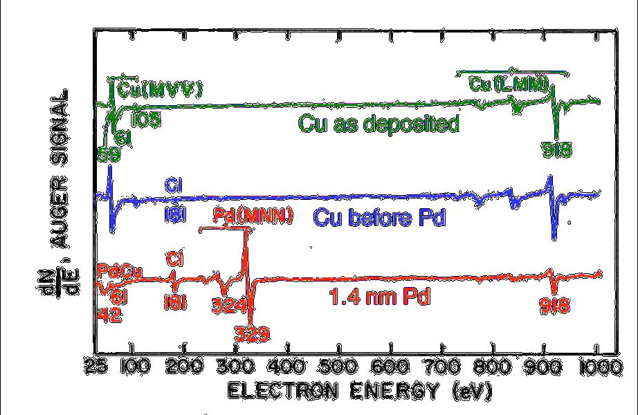
42 Characteristics of AES Auger signal from a substrate is sensitive to presence of surface layers example: Cu versus Pd/Cu (a) freshly deposited Cu (b) Cu prior to Pd deposition (c) after deposition of 1.35 nm Pd Cu signal strongly attenuated by Pd Cu MVV line low-energy completely attenuated 42

43 Example: Cu versus Pd/Cu 43
![Characteristics of AES Cu MVV line (continued) substrate signal decreases as Exp[ x/ ] 60 ev electrons have](/docs-images/93/111905790/images/44-1.jpg "small escape depth Cu LMM line high-energy only partly attenuated 918 ev electrons have larger escape depth")
44 Characteristics of AES Cu MVV line (continued) substrate signal decreases as Exp[ x/ ] 60 ev electrons have small escape depth Cu LMM line high-energy only partly attenuated 918 ev electrons have larger escape depth 44

45 Quantitative Analysis of AES Spectra goal: determine absolute concentration of an element Z from the yield Y A of Auger electrons complications: influence of the matrix on backscattered electrons escape depth consider KLL Auger electrons from thin layer of width depth t t at 45
![Quantitative Analysis of AES Spectra yield: Y A = N Z t e [t] (1 X ) Exp t Cos I[t] T 4 N Z : number of atoms per unit volume; e [t]: ionization cross-section at depth](/docs-images/93/111905790/images/46-1.jpg "t; X : fluorescence yield; : escape depth; : analyzer angle; T : transmission of the analyzer; : solid angle of the analyzer; I[t]: electron excitation flux at depth t.")
46 Quantitative Analysis of AES Spectra yield: Y A = N Z t e [t] (1 X ) Exp t Cos I[t] T 4 N Z : number of atoms per unit volume; e [t]: ionization cross-section at depth t; X : fluorescence yield; : escape depth; : analyzer angle; T : transmission of the analyzer; : solid angle of the analyzer; I[t]: electron excitation flux at depth t. 46
![Quantitative Analysis of AES Spectra separate the excitation flux in to two components: I[t] = I P [t] + I B [t] = I P [t] (1 + R B [t]) I P : flux of primary electrons at depth t; I B : flux of](/docs-images/93/111905790/images/47-1.jpg "backscattered primary electrons; R B : backscattering factor.")
47 Quantitative Analysis of AES Spectra separate the excitation flux in to two components: I[t] = I P [t] + I B [t] = I P [t] (1 + R B [t]) I P : flux of primary electrons at depth t; I B : flux of backscattered primary electrons; R B : backscattering factor. assume external standards with known concentration N S Z concentration NZ T found from of that element in the test sample can be N S Z N T Z = Y T Z Y S Z S T 1 + RS B 1 + R T B ionization cross-sections and fluorescence yields cancel (same atom!) 47
 elemental sensitivities are acquired")
48 Quantitative Analysis of AES Spectra the composition can even be determined directly from the yield ratio when measurements on standard and on specimen are made under the same experimental conditions the composition of the standard is similar the composition of the specimen (otherwise need to consider di erent backscattering yield and di erent escape depth) elemental sensitivities are acquired using pure element standards data are then applied to unknown determinations in multielemental matrices however, need to correct for 48

49 Auger Depth Profiling major use of AES: composition as a function of depth t in thin films Auger signal is generated near the surface ( 3 nm) sputtering provides layer sectioning depth profiles are usually shown as Auger signal height versus sputter time further calibrations required convert sputter time to depth signal height to atomic concentration 49

50 Auger Depth Profiling strong approach for depth profiling: combine AES with RBS RBS: quantitative information on depths heavy-mass constituents without the complications of intermixing often introduced by sputtering ion sputtering causes change in the composition of the surface layers surface segregation preferential sputtering 50

51 Auger Depth Profiling Auger depth profiling better depth resolution than RBS sensitive to heavy and light elements example: RBS and AES data for 100 nm Ni on InP {001}, annealed at 250 C for 30 min RBS spectrum for the as-deposited case: Ni signal superimposed on signal from InP substrate AES spectrum for the as-deposited case In and P signals clearly resolved, comparable heights RBS: Ni/InP interface is sharp (Ni tail: sputtering artifact) 51


52 Example: RBS and AES Data for 100 nm Ni on InP {001} 52
 analysis of the RBS spectra yields P:In ratio of 0.")
53 Example: RBS / AES for 100 nm Ni on InP after annealing: layer is partially reacted with an outer layer of Ni on a layer of In x P y Ni z AES: RBS: Ni layer and reacted In x P y Ni z layer clearly seen in AES P/In yield ratio: 2:1 heights of Ni and In signals nearly equal indicates a Ni:In ratio of 3 (sigma In / Ni 3.08) analysis of the RBS spectra yields P:In ratio of 0.5 di ers from the P-rich composition deduced from AES! 53

54 Example: RBS and AES Data for 100 nm Ni on InP {001} discrepancy due to preferential sputtering and segregation region of pure Ni in the reacted film is better resolved with AES due to its superior depth resolution further, AES would allow determination of e. g. C and O the interface region, which is not possible with RBS advantages of AES: sensitivity to low-mass impurities C, O, common contaminants at surfaces and interfaces presence of such interfacial contaminants plays a disruptive role in thin film reactions by retarding interdi usion degradation of interface planarity on thermal processing 54

55 Example: Sputter Depth Profile of a Ta-Si Film on Polycrystalline Si 55

56 Example: Sputter Depth Profile of a Ta-Si Film on Polycrystalline Si shaded area: O signal from native oxide at the interface removal is crucial for the formatin of a thin, uniform oxide layer on top of the Ta-silicide during thermal oxidation native oxide layer retards release of Si from the poly-si layer leads to oxidation of the whole Ta-silicide layer prevents desired formation of a SiO 2 layer on the surface AES with sputter depth profiling has important applications for multi-layer films AES enables quantitative depth-profiling 56

57 Example: Sputter Depth Profile of a Ta-Si Film on Polycrystalline Si however: sputtering can cause problems preferential sputtering surface roughness rotate the sample during sputtering example: sputter depth profiles of a Cr/Ni multiplayer Cr and Ni are nearby elements in the periodic table sputtering by rastered beam of 5 kev Ar + with and without rotation 57
58 Effect of Surface Roughness 58
Auger Electron Spectroscopy (AES) Prof. Paul K. Chu
 Prof. Paul K. Chu") Auger Electron Spectroscopy (AES) Prof. Paul K. Chu Auger Electron Spectroscopy Introduction Principles Instrumentation Qualitative analysis Quantitative analysis Depth profiling Mapping Examples The Auger
Auger Electron Spectroscopy (AES) Prof. Paul K. Chu Auger Electron Spectroscopy Introduction Principles Instrumentation Qualitative analysis Quantitative analysis Depth profiling Mapping Examples The Auger
Lecture 5. X-ray Photoemission Spectroscopy (XPS)
") Lecture 5 X-ray Photoemission Spectroscopy (XPS) 5. Photoemission Spectroscopy (XPS) 5. Principles 5.2 Interpretation 5.3 Instrumentation 5.4 XPS vs UV Photoelectron Spectroscopy (UPS) 5.5 Auger Electron
Lecture 5 X-ray Photoemission Spectroscopy (XPS) 5. Photoemission Spectroscopy (XPS) 5. Principles 5.2 Interpretation 5.3 Instrumentation 5.4 XPS vs UV Photoelectron Spectroscopy (UPS) 5.5 Auger Electron
5.8 Auger Electron Spectroscopy (AES)
") 5.8 Auger Electron Spectroscopy (AES) 5.8.1 The Auger Process X-ray and high energy electron bombardment of atom can create core hole Core hole will eventually decay via either (i) photon emission (x-ray
5.8 Auger Electron Spectroscopy (AES) 5.8.1 The Auger Process X-ray and high energy electron bombardment of atom can create core hole Core hole will eventually decay via either (i) photon emission (x-ray
IV. Surface analysis for chemical state, chemical composition
 IV. Surface analysis for chemical state, chemical composition Probe beam Detect XPS Photon (X-ray) Photoelectron(core level electron) UPS Photon (UV) Photoelectron(valence level electron) AES electron
Auger Electron Spectroscopy
 Auger Electron Spectroscopy Auger Electron Spectroscopy is an analytical technique that provides compositional information on the top few monolayers of material. Detect all elements above He Detection
An Introduction to Auger Electron Spectroscopy
 An Introduction to Auger Electron Spectroscopy Spyros Diplas MENA3100 SINTEF Materials & Chemistry, Department of Materials Physics & Centre of Materials Science and Nanotechnology, Department of Chemistry,
Introduction to X-ray Photoelectron Spectroscopy (XPS) XPS which makes use of the photoelectric effect, was developed in the mid-1960
 XPS which makes use of the photoelectric effect, was developed in the mid-1960") Introduction to X-ray Photoelectron Spectroscopy (XPS) X-ray Photoelectron Spectroscopy (XPS), also known as Electron Spectroscopy for Chemical Analysis (ESCA) is a widely used technique to investigate
Introduction to X-ray Photoelectron Spectroscopy (XPS) X-ray Photoelectron Spectroscopy (XPS), also known as Electron Spectroscopy for Chemical Analysis (ESCA) is a widely used technique to investigate
Electron Spectroscopy
 Electron Spectroscopy Photoelectron spectroscopy is based upon a single photon in/electron out process. The energy of a photon is given by the Einstein relation : E = h ν where h - Planck constant ( 6.62
Lecture 20 Auger Electron Spectroscopy
 Lecture 20 Auger Electron Spectroscopy Auger history cloud chamber Although Auger emission is intense, it was not used until 1950 s. Evolution of vacuum technology and the application of Auger Spectroscopy
Lecture 17 Auger Electron Spectroscopy
 Lecture 17 Auger Electron Spectroscopy Auger history cloud chamber Although Auger emission is intense, it was not used until 1950 s. Evolution of vacuum technology and the application of Auger Spectroscopy
X-Ray Photoelectron Spectroscopy (XPS)-2
-2") X-Ray Photoelectron Spectroscopy (XPS)-2 Louis Scudiero http://www.wsu.edu/~scudiero; 5-2669 Fulmer 261A Electron Spectroscopy for Chemical Analysis (ESCA) The 3 step model: 1.Optical excitation 2.Transport
X-Ray Photoelectron Spectroscopy (XPS)-2 Louis Scudiero http://www.wsu.edu/~scudiero; 5-2669 Fulmer 261A Electron Spectroscopy for Chemical Analysis (ESCA) The 3 step model: 1.Optical excitation 2.Transport
5) Surface photoelectron spectroscopy. For MChem, Spring, Dr. Qiao Chen (room 3R506) University of Sussex.
 Surface photoelectron spectroscopy. For MChem, Spring, Dr. Qiao Chen (room 3R506) University of Sussex.") For MChem, Spring, 2009 5) Surface photoelectron spectroscopy Dr. Qiao Chen (room 3R506) http://www.sussex.ac.uk/users/qc25/ University of Sussex Today s topics 1. Element analysis with XPS Binding energy,
For MChem, Spring, 2009 5) Surface photoelectron spectroscopy Dr. Qiao Chen (room 3R506) http://www.sussex.ac.uk/users/qc25/ University of Sussex Today s topics 1. Element analysis with XPS Binding energy,
Methods of surface analysis
 Methods of surface analysis Nanomaterials characterisation I RNDr. Věra Vodičková, PhD. Surface of solid matter: last monoatomic layer + absorbed monolayer physical properties are effected (crystal lattice
Auger Electron Spectroscopy Overview
 Auger Electron Spectroscopy Overview Also known as: AES, Auger, SAM 1 Auger Electron Spectroscopy E KLL = E K - E L - E L AES Spectra of Cu EdN(E)/dE Auger Electron E N(E) x 5 E KLL Cu MNN Cu LMM E f E
Auger Electron Spectroscopy *
 OpenStax-CNX module: m43546 1 Auger Electron Spectroscopy * Amanda M. Goodman Andrew R. Barron This work is produced by OpenStax-CNX and licensed under the Creative Commons Attribution License 3.0 1 Basic
MSE 321 Structural Characterization
 Auger Spectroscopy Auger Electron Spectroscopy (AES) Scanning Auger Microscopy (SAM) Incident Electron Ejected Electron Auger Electron Initial State Intermediate State Final State Physical Electronics
Advanced Lab Course. X-Ray Photoelectron Spectroscopy 1 INTRODUCTION 1 2 BASICS 1 3 EXPERIMENT Qualitative analysis Chemical Shifts 7
 Advanced Lab Course X-Ray Photoelectron Spectroscopy M210 As of: 2015-04-01 Aim: Chemical analysis of surfaces. Content 1 INTRODUCTION 1 2 BASICS 1 3 EXPERIMENT 3 3.1 Qualitative analysis 6 3.2 Chemical
Fundamentals of Nanoscale Film Analysis
 Fundamentals of Nanoscale Film Analysis Terry L. Alford Arizona State University Tempe, AZ, USA Leonard C. Feldman Vanderbilt University Nashville, TN, USA James W. Mayer Arizona State University Tempe,
X-ray Photoelectron Spectroscopy (XPS)
") X-ray Photoelectron Spectroscopy (XPS) As part of the course Characterization of Catalysts and Surfaces Prof. Dr. Markus Ammann Paul Scherrer Institut markus.ammann@psi.ch Resource for further reading:
X-ray Photoelectron Spectroscopy (XPS) As part of the course Characterization of Catalysts and Surfaces Prof. Dr. Markus Ammann Paul Scherrer Institut markus.ammann@psi.ch Resource for further reading:
X-Ray Photoelectron Spectroscopy (XPS)-2
-2") X-Ray Photoelectron Spectroscopy (XPS)-2 Louis Scudiero http://www.wsu.edu/~pchemlab ; 5-2669 Fulmer 261A Electron Spectroscopy for Chemical Analysis (ESCA) The 3 step model: 1.Optical excitation 2.Transport
X-Ray Photoelectron Spectroscopy (XPS)-2 Louis Scudiero http://www.wsu.edu/~pchemlab ; 5-2669 Fulmer 261A Electron Spectroscopy for Chemical Analysis (ESCA) The 3 step model: 1.Optical excitation 2.Transport
Auger Electron Spectroscopy (AES)
") 1. Introduction Auger Electron Spectroscopy (AES) Silvia Natividad, Gabriel Gonzalez and Arena Holguin Auger Electron Spectroscopy (Auger spectroscopy or AES) was developed in the late 1960's, deriving
1. Introduction Auger Electron Spectroscopy (AES) Silvia Natividad, Gabriel Gonzalez and Arena Holguin Auger Electron Spectroscopy (Auger spectroscopy or AES) was developed in the late 1960's, deriving
X-Ray Photoelectron Spectroscopy (XPS) Auger Electron Spectroscopy (AES)
 Auger Electron Spectroscopy (AES)") X-Ray Photoelectron Spectroscopy (XPS) Auger Electron Spectroscopy (AES) XPS X-ray photoelectron spectroscopy (XPS) is one of the most used techniques to chemically characterize the surface. Also known
X-Ray Photoelectron Spectroscopy (XPS) Auger Electron Spectroscopy (AES) XPS X-ray photoelectron spectroscopy (XPS) is one of the most used techniques to chemically characterize the surface. Also known
Fig 1: Auger Electron Generation (a) Step 1 and (b) Step 2
 Step 1 and (b) Step 2") Auger Electron Spectroscopy (AES) Physics of AES: Auger Electrons were discovered in 1925 but were used in surface analysis technique in 1968. Auger Electron Spectroscopy (AES) is a very effective method
Auger Electron Spectroscopy (AES) Physics of AES: Auger Electrons were discovered in 1925 but were used in surface analysis technique in 1968. Auger Electron Spectroscopy (AES) is a very effective method
8.6 Relaxation Processes
 CHAPTER 8. INNER SHELLS 175 Figure 8.17: Splitting of the 3s state in Fe which is missing in Zn. Refs. [12,13]. be aligned parallel or antiparallel with the spins of the 3d electrons of iron. 13 Thus we
Electron Spettroscopies
 Electron Spettroscopies Spettroscopy allows to characterize a material from the point of view of: chemical composition, electronic states and magnetism, electronic, roto-vibrational and magnetic excitations.
Name: (a) What core levels are responsible for the three photoelectron peaks in Fig. 1?
 What core levels are responsible for the three photoelectron peaks in Fig. 1?") Physics 243A--Surface Physics of Materials: Spectroscopy Final Examination December 16, 2014 (3 problems, 100 points total, open book, open notes and handouts) Name: [1] (50 points), including Figures
Physics 243A--Surface Physics of Materials: Spectroscopy Final Examination December 16, 2014 (3 problems, 100 points total, open book, open notes and handouts) Name: [1] (50 points), including Figures
Photoemission Spectroscopy
 FY13 Experimental Physics - Auger Electron Spectroscopy Photoemission Spectroscopy Supervisor: Per Morgen SDU, Institute of Physics Campusvej 55 DK - 5250 Odense S Ulrik Robenhagen,
EDS User School. Principles of Electron Beam Microanalysis
 EDS User School Principles of Electron Beam Microanalysis Outline 1.) Beam-specimen interactions 2.) EDS spectra: Origin of Bremsstrahlung and characteristic peaks 3.) Moseley s law 4.) Characteristic
X-Ray Photoelectron Spectroscopy (XPS)
") X-Ray Photoelectron Spectroscopy (XPS) Louis Scudiero http://www.wsu.edu/~scudiero; 5-2669 Electron Spectroscopy for Chemical Analysis (ESCA) The basic principle of the photoelectric effect was enunciated
X-Ray Photoelectron Spectroscopy (XPS) Louis Scudiero http://www.wsu.edu/~scudiero; 5-2669 Electron Spectroscopy for Chemical Analysis (ESCA) The basic principle of the photoelectric effect was enunciated
Appearance Potential Spectroscopy
 Appearance Potential Spectroscopy Submitted by Sajanlal P. R CY06D009 Sreeprasad T. S CY06D008 Dept. of Chemistry IIT MADRAS February 2006 1 Contents Page number 1. Introduction 3 2. Theory of APS 3 3.
Secondary Ion Mass Spectrometry (SIMS)
") CHEM53200: Lecture 10 Secondary Ion Mass Spectrometry (SIMS) Major reference: Surface Analysis Edited by J. C. Vickerman (1997). 1 Primary particles may be: Secondary particles can be e s, neutral species
CHEM53200: Lecture 10 Secondary Ion Mass Spectrometry (SIMS) Major reference: Surface Analysis Edited by J. C. Vickerman (1997). 1 Primary particles may be: Secondary particles can be e s, neutral species
X-Ray Photoelectron Spectroscopy (XPS) Prof. Paul K. Chu
 Prof. Paul K. Chu") X-Ray Photoelectron Spectroscopy (XPS) Prof. Paul K. Chu X-ray Photoelectron Spectroscopy Introduction Qualitative analysis Quantitative analysis Charging compensation Small area analysis and XPS imaging
X-Ray Photoelectron Spectroscopy (XPS) Prof. Paul K. Chu X-ray Photoelectron Spectroscopy Introduction Qualitative analysis Quantitative analysis Charging compensation Small area analysis and XPS imaging
X-Ray Photoelectron Spectroscopy (XPS)
") X-Ray Photoelectron Spectroscopy (XPS) Louis Scudiero http://www.wsu.edu/~scudiero; 5-2669 Fulmer 261A Electron Spectroscopy for Chemical Analysis (ESCA) The basic principle of the photoelectric effect
X-Ray Photoelectron Spectroscopy (XPS) Louis Scudiero http://www.wsu.edu/~scudiero; 5-2669 Fulmer 261A Electron Spectroscopy for Chemical Analysis (ESCA) The basic principle of the photoelectric effect
Ma5: Auger- and Electron Energy Loss Spectroscopy
 Ma5: Auger- and Electron Energy Loss Spectroscopy 1 Introduction Electron spectroscopies, namely Auger electron- and electron energy loss spectroscopy are utilized to determine the KLL spectrum and the
Generation of X-Rays in the SEM specimen
 Generation of X-Rays in the SEM specimen The electron beam generates X-ray photons in the beam-specimen interaction volume beneath the specimen surface. Some X-ray photons emerging from the specimen have
MT Electron microscopy Scanning electron microscopy and electron probe microanalysis
 MT-0.6026 Electron microscopy Scanning electron microscopy and electron probe microanalysis Eero Haimi Research Manager Outline 1. Introduction Basics of scanning electron microscopy (SEM) and electron
X-ray Energy Spectroscopy (XES).
.") X-ray Energy Spectroscopy (XES). X-ray fluorescence as an analytical tool for element analysis is based on 3 fundamental parameters: A. Specificity: In determining an x-ray emission energy E certainty
X-ray Energy Spectroscopy (XES). X-ray fluorescence as an analytical tool for element analysis is based on 3 fundamental parameters: A. Specificity: In determining an x-ray emission energy E certainty
MSE 321 Structural Characterization
 Auger Spectroscopy Auger Electron Spectroscopy (AES) Scanning Auger Microscopy (SAM) Incident Electron Ejected Electron Auger Electron Initial State Intermediate State Final State Physical Electronics
AES - Auger Electron Spectrosopy
 Advanced Materials - Lab Intermediate Physics Ulm University Institute of Solid State Physics AES - Auger Electron Spectrosopy Sebastian Schnurr March 13, 2013 Safety Precautions MAKE SURE THAT YOU UNDERSTAND
QUESTIONS AND ANSWERS
 QUESTIONS AND ANSWERS (1) For a ground - state neutral atom with 13 protons, describe (a) Which element this is (b) The quantum numbers, n, and l of the inner two core electrons (c) The stationary state
The Benefit of Wide Energy Range Spectrum Acquisition During Sputter Depth Profile Measurements
 The Benefit of Wide Energy Range Spectrum Acquisition During Sputter Depth Profile Measurements Uwe Scheithauer, 82008 Unterhaching, Germany E-Mail: scht.uhg@googlemail.com Internet: orcid.org/0000-0002-4776-0678;
Lecture 5-8 Instrumentation
 Lecture 5-8 Instrumentation Requirements 1. Vacuum Mean Free Path Contamination Sticking probability UHV Materials Strength Stability Permeation Design considerations Pumping speed Virtual leaks Leaking
Birck Nanotechnology Center XPS: X-ray Photoelectron Spectroscopy ESCA: Electron Spectrometer for Chemical Analysis
 Birck Nanotechnology Center XPS: X-ray Photoelectron Spectroscopy ESCA: Electron Spectrometer for Chemical Analysis Dmitry Zemlyanov Birck Nanotechnology Center, Purdue University Outline Introduction
Rutherford Backscattering Spectrometry
 Rutherford Backscattering Spectrometry EMSE-515 Fall 2005 F. Ernst 1 Bohr s Model of an Atom existence of central core established by single collision, large-angle scattering of alpha particles ( 4 He
Lecture 22 Ion Beam Techniques
 Lecture 22 Ion Beam Techniques Schroder: Chapter 11.3 1/44 Announcements Homework 6/6: Will be online on later today. Due Wednesday June 6th at 10:00am. I will return it at the final exam (14 th June).
AUGER ELECTRON SPECTROSCOPY
 CHAPTER 10 AUGER ELECTRON SPECTROSCOPY Richard P. Gunawardane and Christopher R. Arumainayagam Department of Chemistry, Wellesley College, Wellesley, MA 02481, U.S.A. 10.1 INTRODUCTION Auger electron spectroscopy
4. Inelastic Scattering
 1 4. Inelastic Scattering Some inelastic scattering processes A vast range of inelastic scattering processes can occur during illumination of a specimen with a highenergy electron beam. In principle, many
Photoelectron Spectroscopy. Xiaozhe Zhang 10/03/2014
 Photoelectron Spectroscopy Xiaozhe Zhang 10/03/2014 A conception last time remain Secondary electrons are electrons generated as ionization products. They are called 'secondary' because they are generated
Auger & X-ray Fluorescence
 At low energies or low temperature gas (plasma) the primary processes are photoionzation or excitation by particles (electron, atom, proton). Recombination takes place with emission of photons. In hot
Photon Interaction. Spectroscopy
 Photon Interaction Incident photon interacts with electrons Core and Valence Cross Sections Photon is Adsorbed Elastic Scattered Inelastic Scattered Electron is Emitted Excitated Dexcitated Stöhr, NEXAPS
Saturation Absorption Spectroscopy of Rubidium Atom
 Saturation Absorption Spectroscopy of Rubidium Atom Jayash Panigrahi August 17, 2013 Abstract Saturated absorption spectroscopy has various application in laser cooling which have many relevant uses in
Table 1: Residence time (τ) in seconds for adsorbed molecules
 in seconds for adsorbed molecules") 1 Surfaces We got our first hint of the importance of surface processes in the mass spectrum of a high vacuum environment. The spectrum was dominated by water and carbon monoxide, species that represent
1 Surfaces We got our first hint of the importance of surface processes in the mass spectrum of a high vacuum environment. The spectrum was dominated by water and carbon monoxide, species that represent
Energy Spectroscopy. Ex.: Fe/MgO
 Energy Spectroscopy Spectroscopy gives access to the electronic properties (and thus chemistry, magnetism,..) of the investigated system with thickness dependence Ex.: Fe/MgO Fe O Mg Control of the oxidation
Energy Spectroscopy. Excitation by means of a probe
 Energy Spectroscopy Excitation by means of a probe Energy spectral analysis of the in coming particles -> XAS or Energy spectral analysis of the out coming particles Different probes are possible: Auger
X-Ray transitions to low lying empty states
 X-Ray Spectra: - continuous part of the spectrum is due to decelerated electrons - the maximum frequency (minimum wavelength) of the photons generated is determined by the maximum kinetic energy of the
Characterization of Secondary Emission Materials for Micro-Channel Plates. S. Jokela, I. Veryovkin, A. Zinovev
 Characterization of Secondary Emission Materials for Micro-Channel Plates S. Jokela, I. Veryovkin, A. Zinovev Secondary Electron Yield Testing Technique We have incorporated XPS, UPS, Ar-ion sputtering,
ECE Semiconductor Device and Material Characterization
 ECE 4813 Semiconductor Device and Material Characterization Dr. Alan Doolittle School of Electrical and Computer Engineering Georgia Institute of Technology As with all of these lecture slides, I am indebted
MS482 Materials Characterization ( 재료분석 ) Lecture Note 2: UPS
 Lecture Note 2: UPS") 2016 Fall Semester MS482 Materials Characterization ( 재료분석 ) Lecture Note 2: UPS Byungha Shin Dept. of MSE, KAIST 1 Course Information Syllabus 1. Overview of various characterization techniques (1 lecture)
2016 Fall Semester MS482 Materials Characterization ( 재료분석 ) Lecture Note 2: UPS Byungha Shin Dept. of MSE, KAIST 1 Course Information Syllabus 1. Overview of various characterization techniques (1 lecture)
MT Electron microscopy Scanning electron microscopy and electron probe microanalysis
 MT-0.6026 Electron microscopy Scanning electron microscopy and electron probe microanalysis Eero Haimi Research Manager Outline 1. Introduction Basics of scanning electron microscopy (SEM) and electron
X- ray Photoelectron Spectroscopy and its application in phase- switching device study
 X- ray Photoelectron Spectroscopy and its application in phase- switching device study Xinyuan Wang A53073806 I. Background X- ray photoelectron spectroscopy is of great importance in modern chemical and
ATOMIC STRUCTURE, ELECTRONS, AND PERIODICITY
 ATOMIC STRUCTURE, ELECTRONS, AND PERIODICITY All matter is made of atoms. There are a limited number of types of atoms; these are the elements. (EU 1.A) Development of Atomic Theory Atoms are so small
EE 527 MICROFABRICATION. Lecture 5 Tai-Chang Chen University of Washington
 EE 527 MICROFABRICATION Lecture 5 Tai-Chang Chen University of Washington MICROSCOPY AND VISUALIZATION Electron microscope, transmission electron microscope Resolution: atomic imaging Use: lattice spacing.
Reduced preferential sputtering of TiO 2 (and Ta 2 O 5 ) thin films through argon cluster ion bombardment.
 thin films through argon cluster ion bombardment.") NATIOMEM Reduced preferential sputtering of TiO 2 (and Ta 2 O 5 ) thin films through argon cluster ion bombardment. R. Grilli *, P. Mack, M.A. Baker * * University of Surrey, UK ThermoFisher Scientific
NATIOMEM Reduced preferential sputtering of TiO 2 (and Ta 2 O 5 ) thin films through argon cluster ion bombardment. R. Grilli *, P. Mack, M.A. Baker * * University of Surrey, UK ThermoFisher Scientific
X-Ray Photoelectron Spectrometry (XPS) Electron Spectroscopy for Chemical Analysis (ECSA) Principle of XPS. Comparison of Surface Analysis Techniques
 Electron Spectroscopy for Chemical Analysis (ECSA) Principle of XPS. Comparison of Surface Analysis Techniques") Comparison of Surface Analysis Techniques X-Ray Photoelectron Spectrometry (XPS) Electron Spectroscopy for Chemical Analysis (ECSA)!! AES! XPS! TOF-SIMS! D-SIMS Probe Beam!! Electrons! Photons! Ions! Ions!
Comparison of Surface Analysis Techniques X-Ray Photoelectron Spectrometry (XPS) Electron Spectroscopy for Chemical Analysis (ECSA)!! AES! XPS! TOF-SIMS! D-SIMS Probe Beam!! Electrons! Photons! Ions! Ions!
Chemical Analysis in TEM: XEDS, EELS and EFTEM. HRTEM PhD course Lecture 5
 Chemical Analysis in TEM: XEDS, EELS and EFTEM HRTEM PhD course Lecture 5 1 Part IV Subject Chapter Prio x-ray spectrometry 32 1 Spectra and mapping 33 2 Qualitative XEDS 34 1 Quantitative XEDS 35.1-35.4
Spectroscopy. Practical Handbook of. J. W. Robinson, Ph.D., D.Sc, F.R.C.S. Department of Chemistry Louisiana State University Baton Rouge, Louisiana
 Practical Handbook of Spectroscopy Edited by J. W. Robinson, Ph.D., D.Sc, F.R.C.S. Department of Chemistry Louisiana State University Baton Rouge, Louisiana CRC Press Boca Raton Ann Arbor Boston TABLE
Spectroscopy on Mars!
 Spectroscopy on Mars! Pathfinder Spirit and Opportunity Real World Friday H2A The Mars Pathfinder: Geological Elemental Analysis On December 4th, 1996, the Mars Pathfinder was launched from earth to begin
Photoelectron spectroscopy Instrumentation. Nanomaterials characterization 2
 Photoelectron spectroscopy Instrumentation Nanomaterials characterization 2 RNDr. Věra V Vodičkov ková,, PhD. Photoelectron Spectroscopy general scheme Impact of X-ray emitted from source to the sample
MODERN TECHNIQUES OF SURFACE SCIENCE
 MODERN TECHNIQUES OF SURFACE SCIENCE Second edition D. P. WOODRUFF & T. A. DELCHAR Department ofphysics, University of Warwick CAMBRIDGE UNIVERSITY PRESS Contents Preface to first edition Preface to second
MS482 Materials Characterization ( 재료분석 ) Lecture Note 5: RBS
 Lecture Note 5: RBS") 2016 Fall Semester MS482 Materials Characterization ( 재료분석 ) Lecture Note 5: RBS Byungha Shin Dept. of MSE, KAIST 1 Course Information Syllabus 1. Overview of various characterization techniques (1 lecture)
2016 Fall Semester MS482 Materials Characterization ( 재료분석 ) Lecture Note 5: RBS Byungha Shin Dept. of MSE, KAIST 1 Course Information Syllabus 1. Overview of various characterization techniques (1 lecture)
X-ray photoelectron spectroscopy - An introduction
 X-ray photoelectron spectroscopy - An introduction Spyros Diplas spyros.diplas@sintef.no spyros.diplas@smn.uio.no SINTEF Materials & Chemistry, Materials Physics -Oslo & Centre of Materials Science and
X-ray Spectroscopy. Interaction of X-rays with matter XANES and EXAFS XANES analysis Pre-edge analysis EXAFS analysis
 X-ray Spectroscopy Interaction of X-rays with matter XANES and EXAFS XANES analysis Pre-edge analysis EXAFS analysis Element specific Sensitive to low concentrations (0.01-0.1 %) Why XAS? Applicable under
Chapter 9. Electron mean free path Microscopy principles of SEM, TEM, LEEM
 Chapter 9 Electron mean free path Microscopy principles of SEM, TEM, LEEM 9.1 Electron Mean Free Path 9. Scanning Electron Microscopy (SEM) -SEM design; Secondary electron imaging; Backscattered electron
MS482 Materials Characterization ( 재료분석 ) Lecture Note 4: XRF
 Lecture Note 4: XRF") 2016 Fall Semester MS482 Materials Characterization ( 재료분석 ) Lecture Note 4: XRF Byungha Shin Dept. of MSE, KAIST 1 Course Information Syllabus 1. Overview of various characterization techniques (1 lecture)
2016 Fall Semester MS482 Materials Characterization ( 재료분석 ) Lecture Note 4: XRF Byungha Shin Dept. of MSE, KAIST 1 Course Information Syllabus 1. Overview of various characterization techniques (1 lecture)
ATOMIC STRUCTURE, ELECTRONS, AND PERIODICITY
 ATOMIC STRUCTURE, ELECTRONS, AND PERIODICITY All matter is made of atoms. There are a limited number of types of atoms; these are the elements. (EU 1.A) Development of Atomic Theory Atoms are so small
Electronic Structure of Atoms. Chapter 6
 Electronic Structure of Atoms Chapter 6 Electronic Structure of Atoms 1. The Wave Nature of Light All waves have: a) characteristic wavelength, λ b) amplitude, A Electronic Structure of Atoms 1. The Wave
Practical Surface Analysis
 Practical Surface Analysis SECOND EDITION Volume 1 Auger and X-ray Photoelectron Spectroscopy Edited by D. BRIGGS ICI PLC, Wilton Materials Research Centre, Wilton, Middlesbrough, Cleveland, UK and M.
PHYS 219 General Physics: Electricity, Light and Modern Physics
 PHYS 219 General Physics: Electricity, Light and Modern Physics Final exam is scheduled on Thursday May 2 @ 8 10 AM In Physics 112 It will cover five Chapters 25, 27, 28, 29, and 30. Review lecture notes,
Experimental 2.1 Introduction. Ultra high vacuum.
 2 Experimental 2.1 Introduction. Ultra high vacuum. The interest in solid-gas (or solid-vacuum) interfaces has been increasing rapidly during the last three decades. On one hand this is due to the practical
CHARACTERIZATION of NANOMATERIALS KHP
 CHARACTERIZATION of NANOMATERIALS Overview of the most common nanocharacterization techniques MAIN CHARACTERIZATION TECHNIQUES: 1.Transmission Electron Microscope (TEM) 2. Scanning Electron Microscope
Key Equations. Determining the smallest change in an atom's energy.
 ATOMIC STRUCTURE AND PERIODICITY Matter and Energy Key Equations λν = c ΔE = hν Relating speed of a wave to its wavelength and frequency. Determining the smallest change in an atom's energy. H( λ =R n
Photoelectron Peak Intensities in Solids
 Photoelectron Peak Intensities in Solids Electronic structure of solids Photoelectron emission through solid Inelastic scattering Other excitations Intrinsic and extrinsic Shake-up, shake-down and shake-off
Chapter Six: X-Rays. 6.1 Discovery of X-rays
 Chapter Six: X-Rays 6.1 Discovery of X-rays In late 1895, a German physicist, W. C. Roentgen was working with a cathode ray tube in his laboratory. He was working with tubes similar to our fluorescent
Particle Behavior of Light 1. Calculate the energy of a photon, mole of photons 2. Find binding energy of an electron (know KE) 3. What is a quanta?
 3. What is a quanta?") Properties of Electromagnetic Radiation 1. What is spectroscopy, a continuous spectrum, a line spectrum, differences and similarities 2. Relationship of wavelength to frequency, relationship of E to λ
Properties of Electromagnetic Radiation 1. What is spectroscopy, a continuous spectrum, a line spectrum, differences and similarities 2. Relationship of wavelength to frequency, relationship of E to λ
Inelastic soft x-ray scattering, fluorescence and elastic radiation
 Inelastic soft x-ray scattering, fluorescence and elastic radiation What happens to the emission (or fluorescence) when the energy of the exciting photons changes? The emission spectra (can) change. One
X-ray Photoemission Spectroscopy (XPS - Ma4)
") Master Laboratory Report X-ray Photoemission Spectroscopy (XPS - Ma4) Supervisor: Andrew Britton Students: Dachi Meurmishvili, Muhammad Khurram Riaz and Martin Borchert Date: November 17th 2016 1 Contents
Master Laboratory Report X-ray Photoemission Spectroscopy (XPS - Ma4) Supervisor: Andrew Britton Students: Dachi Meurmishvili, Muhammad Khurram Riaz and Martin Borchert Date: November 17th 2016 1 Contents
Probing Matter: Diffraction, Spectroscopy and Photoemission
 Probing Matter: Diffraction, Spectroscopy and Photoemission Anders Nilsson Stanford Synchrotron Radiation Laboratory Why X-rays? VUV? What can we hope to learn? 1 Photon Interaction Incident photon interacts
Auger Analyses Using Low Angle Incident Electrons
 Auger Analyses Using Low Angle Incident Electrons Kenichi Tsutsumi, Yuji agasawa and Toyohiko Tazawa Electron ptics Division, JEL Ltd. Introduction Auger Electron Spectroscopy (AES) is widely used, as
Atomic Structure & Radiative Transitions
 Atomic Structure & Radiative Transitions electron kinetic energy nucleus-electron interaction electron-electron interaction Remember the meaning of spherical harmonics Y l, m (θ, ϕ) n specifies the
Lecture 11 Surface Characterization of Biomaterials in Vacuum
 1 Lecture 11 Surface Characterization of Biomaterials in Vacuum The structure and chemistry of a biomaterial surface greatly dictates the degree of biocompatibility of an implant. Surface characterization
Within the vast field of atomic physics, collisions of heavy ions with atoms define
 Chapter 1 Introduction Within the vast field of atomic physics, collisions of heavy ions with atoms define one of the most active areas of research. In the last decades, the design and construction of
ToF-SIMS or XPS? Xinqi Chen Keck-II
 ToF-SIMS or XPS? Xinqi Chen Keck-II 1 Time of Flight Secondary Ion Mass Spectrometry (ToF-SIMS) Not ToF MS (laser, solution) X-ray Photoelectron Spectroscopy (XPS) 2 3 Modes of SIMS 4 Secondary Ion Sputtering
Spectroscopy of Nanostructures. Angle-resolved Photoemission (ARPES, UPS)
") Spectroscopy of Nanostructures Angle-resolved Photoemission (ARPES, UPS) Measures all quantum numbers of an electron in a solid. E, k x,y, z, point group, spin E kin, ϑ,ϕ, hν, polarization, spin Electron
Spectroscopy of Nanostructures Angle-resolved Photoemission (ARPES, UPS) Measures all quantum numbers of an electron in a solid. E, k x,y, z, point group, spin E kin, ϑ,ϕ, hν, polarization, spin Electron
Core Level Spectroscopies
 Core Level Spectroscopies Spectroscopies involving core levels are element-sensitive, and that makes them very useful for understanding chemical bonding, as well as for the study of complex materials.
COLLEGE PHYSICS. Chapter 30 ATOMIC PHYSICS
 COLLEGE PHYSICS Chapter 30 ATOMIC PHYSICS Matter Waves: The de Broglie Hypothesis The momentum of a photon is given by: The de Broglie hypothesis is that particles also have wavelengths, given by: Matter
PHI 5000 Versaprobe-II Focus X-ray Photo-electron Spectroscopy
 PHI 5000 Versaprobe-II Focus X-ray Photo-electron Spectroscopy The very basic theory of XPS XPS theroy Surface Analysis Ultra High Vacuum (UHV) XPS Theory XPS = X-ray Photo-electron Spectroscopy X-ray
Introduction to SIMS Basic principles Components Techniques Drawbacks Figures of Merit Variations Resources
 Introduction to SIMS Basic principles Components Techniques Drawbacks Figures of Merit Variations Resources New technique for surface chemical analysis. SIMS examines the mass of ions, instead of energy
Chapter 6: Electronic Structure of Atoms
 Chapter 6: Electronic Structure of Atoms Learning Outcomes: Calculate the wavelength of electromagnetic radiation given its frequency or its frequency given its wavelength. Order the common kinds of radiation
Scanning Auger Microprobe
 Scanning Auger Microprobe This enables images of the elements in the near surface layer of samples to be acquired. SAM a combination of the techniques of SEM and AES. An electron beam is scanned over the
Ultimate Lateral Resolution in Electron Microscopy by FE-Auger
 Ultimate Lateral Resolution in Electron Microscopy by FE-Auger P. Bouckenooge, H. Terryn, I. Vandendael Research Group of Electrochemical and Surface Engineering (SURF), Vrije Universiteit Brussel (VUB),