Surface Analysis. Dr. Lynn Fuller Dr. Fuller s Webpage:
|
|
|
- Laurence O’Neal’
- 6 years ago
- Views:
Transcription
1 ROCHESTER INSTITUTE OF TECHNOLOGY MICROELECTRONIC ENGINEERING Surface Analysis Dr. Lynn Fuller Dr. Fuller s Webpage: 82 Lomb Memorial Drive Rochester, NY Tel (585) Fax (585) Lynn.Fuller@rit.edu MicroE webpage: Surface.ppt Page 1
2 OUTLINE Introduction Scanning Electron Microscopy (SEM) Transmission Electron Microscopy (TEM) Atomic Force Microscopy (AFM) Energy Dispersive Analysis of x-rays (EDAX) Auger Electron Spectroscopy X-ray Fluorescence Spectroscopy (XPS) Secondary Ion Mass Spectroscopy (SIMS) Capacitance Voltage Measurements Surface Charge Analyzer Page 2
3 INTRODUCTION Surface analysis refers to a collection of techniques to get information about the chemical or physical nature of a surface. (few µm) Page 3

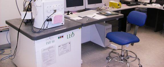
4 LEO EVO 50 Page 4

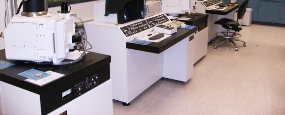
5 AMRAY & 2 Page 5
6 SCANNING ELECTRON MICROSCOPE (SEM) Auger Electrons 10Å 1 µm Primary Electron Beam V V +200 V hv Secondary V Electrons, 20Å V Sintillator (Phosphor Coated) Back scattered Electrons Characteristic X-rays X-Ray Continuum R Vout Photo multiplier Tube (low work Function) Specimen Current Detector Page 6


7 TRANSMISSION ELECTRON MICROSCOPE Specimen Support Grid +200 V Primary Electron Beam V Sintillator (Phosphor Coated) V V V Very Thin Specimen < 1 µm Photo multiplier Tube (low work Function) R Vout Page 7


8 TEM OF MOS STRUCTURE POLY SiO2 Si Page 8


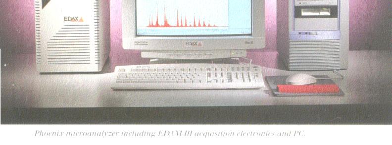
9 LEO EVO 50 SEM & EDAX Page 9

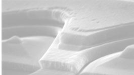
10 SEM EXAMPLES Page 10
11 SEM EXAMPLES Page 11

")
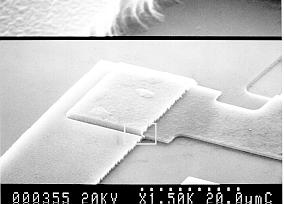
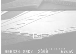
12 SEM WITH FOCUSED ION BEAM (FIB) Page 12
 FIB")


13 SEM WITH FOCUSED ION BEAM (FIB) FIB allows crossection SEM images to be made at any point by cutting a trench with a focused beam of argon ions. Page 13


14 SCANNING TUNNELING MICROSCOPE (STM) Z X Y ~ 100 Å Gap Surface I Piezoelectric Motors Scan Tip in X and Y, Electronics control Z such that the Tunneling Current I is Constant. The Control Voltage for Z is a Measure of Surface Topology Page 14

15 ATOMIC FORCE MICROSCOPE (AFM) Page 15
 Flared tip able to measure undercut sidewalls Used in non-contact mode")
16 ATOMIC FORCE MICROSCOPE (AFM) Standard Sharp Apex Slender Long Used in Contact mode CD Mode (Conical and Flared) Flared tip able to measure undercut sidewalls Used in non-contact mode Page 16
17 ENERGY DISPERSIVE ANALYSIS OF XRAYS (EDAX) Auger Electrons 10Å 1 µm Primary Electron Beam Secondary Electrons, 20Å Back scattered Electrons Characteristic X-rays X-Ray Continuum Page 17
18 ENERGY DISPERSIVE ANALYSIS OF XRAYS (EDAX) PRIMARY ELECTRON IRON Atomic Number 26 En = Z 2 /n 2 E1 = ev E2 = ev E3 = ev L M K K Β x-ray E =h ν or λ=h c / E Notation: K x-rays are associated with transitions to 1st shell, L x-rays to the 2nd shell. α x-rays are between adjacent shells, Β x-rays are two shells apart, etc. Page 18
19 EDAX Crystal Detector Cryogenic Semiconductor Detector Liquid Nitrogen Cooled Semiconductor Detector Page 19

20 EDAX Page 20
21 EDAX Page 21


22 EDAX ANALYSIS OF FAILED RF PIN B A Failed RF Pin: 40X Failed RF Pin: 320X Point A & B Analyzed using EDAX Page 22
23 COUNTS MLK MODE SELECT ELEMENT LK Z=30 ZN PR=S 319 SEC 0 INT V=4096 H=20KEV 1:1 AQ=20KEV 1H POINT B COUNTS MLK MODE SELECT ELEMENT ML Z=80 HG PR=S 150 SEC 0 INT V=4096 H=20KEV 1:1 AQ=20KEV 1H POINT A 20.48KEV 20.48KEV ENERGY KEV ENERGY KEV COUNTS MLK MODE SELECT ELEMENT LK Z=29 CU PR=S 319 SEC 0 INT V=4096 H=20KEV 1:1 AQ=20KEV 1H COUNTS MLK MODE SELECT ELEMENT MLK Z=41 NB PR=S 150 SEC 0 INT V=4096 H=20KEV 1:1 AQ=20KEV 1H POINT B 20.48KEV POINT A 20.48KEV ENERGY KEV ENERGY KEV
24 AUGER ELECTRON SPECTROSCOPY Auger Electrons 10Å 1 µm Primary Electron Beam Secondary Electrons, 20Å Back scattered Electrons Characteristic X-rays X-Ray Continuum Page 24

25 AUGER Page 25


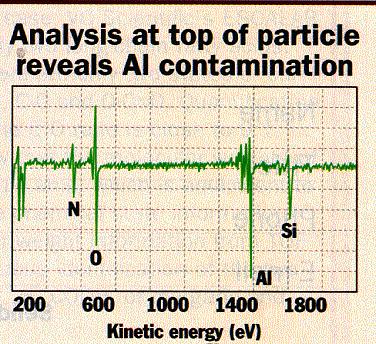
26 AUGER Auger analysis showed an aluminum particle contaminated the wafer. Page 26
 http://www.cea.com/cai/augtheo/process.")
27 AUGER Simultaneous Process Ionization of Core Electron Upper level electron falls into lower energy state Energy release from second electron allows Auger electron to escape The illustrated LMM Auger electron energy is ~423 ev (EAuger = EL2 - EM4 - EM3) Page 27


28 Chart of principal Auger electron energies Dots indicate electron energies for principal Auger peaks for each element Surface Analysis AUGER Page 28

 or X-ray Photo")
 X-ray Source")
29 ESCA or XPS Electron Spectroscopy for Chemical Analysis (ESCA) or X-ray Photo Electron Spectroscopy (XPS) X-ray Source Electrons Sample Page 29

30 SECONDARY ION MASS SPECTROSCOPY (SIMS) Ion Beam Gun Mass Spectrometer Sample Page 30
31 RESIDUAL GAS ANALYZER (RGA) The Quadrupole Filter has voltages such that down the center there is a zero potential equipotential surface. Only ions of a certain mass make it all the way to the photomultiplier tube. The voltage applied to the filter at radio frequency and DC selects the mass. Gas Sample Quadrupole Filter Filiment Lens Quadrupole Filter Photomultiplier Tube R Vout Page 31

32 RGA Page 32
33 CAPACITANCE VOLTAGE MEASUREMENTS -10 < V < +10 Metal Oxide, Xox silicon Cox= εo εr Area/Xox Apply a DC voltage (V) to the capacitor and measure the capacitance. High frequency and low frequency capacitance measurement techniques are available. Page 33
34 CV MEASUREMENTS Low Frequency Depletion C N-Type Silicon Inversion C FB Accumulation High Frequency V T V FB 0 C min V P-Type Silicon Depletion Accumulation C C FB Low Frequency Inversion C min V FB V T 0 High Frequency V Page 34
35 SCA Capacitive Pickup Signal Amplifier High Voltage Amplifier Light Controller and Modulator Data Acquisition Computer LED Light Source Guard Electrode Silicon Oxide Page 35
36 P-type Wafer Surface Analysis SCA Inversion Wd W T W mid gap N-type Wafer Accumulation + W FB - Qind 0 Wd Inversion W T W mid gap Accumulation - 0 W FB + Qind Page 36
 PROGRAM = FAC-P or FAC-N LOT ID =")
 <F12> start test and wait for measurement <Print Screen> print results <F8>")
37 SCA-2500 SETUP Login: FACTORY Password: OPER <F1> Operate <F1> Test Place the blank spot in middle of wafer on center of the stage Select (use arrow keys, space bar, page up, etc) PROGRAM = FAC-P or FAC-N LOT ID = F WAFER NO. = D1 TOX = 463 (from nanospec) <F12> start test and wait for measurement <Print Screen> print results <F8> exit and log off <ESC> can be used anytime, but wait for current test to be completed Page 37
38 EXAMPLE OF SCA OUTPUT MEASURED AT RIT Page 38


39 EXAMPLE OF SCA OUTPUT MEASURED AT RIT Page 39
40 REFERENCES 1. Scanning Electron Microscopy, Michael T. Postek, et, al., Ladd Research Industries, Inc., Micro-X7000 Operating Manual, Kevex Corporation, 1101 Chess Drive, Foster City, CA 94404, EDAX Inc., 91 McKee Drive, Mahwah, NJ , Tel (201) AFM see, and Page 40
41 HOMEWORK: SURFACE 1. Calculate the wavelength of the K α and L Β x-ray for copper.] 2. Explain how SIMS gives doping profiles. 3. Why can t Auger and a ESCA give doping profiles. Page 41
Imaging Methods: Scanning Force Microscopy (SFM / AFM)
") Imaging Methods: Scanning Force Microscopy (SFM / AFM) The atomic force microscope (AFM) probes the surface of a sample with a sharp tip, a couple of microns long and often less than 100 Å in diameter.
Imaging Methods: Scanning Force Microscopy (SFM / AFM) The atomic force microscope (AFM) probes the surface of a sample with a sharp tip, a couple of microns long and often less than 100 Å in diameter.
ECE Semiconductor Device and Material Characterization
 ECE 4813 Semiconductor Device and Material Characterization Dr. Alan Doolittle School of Electrical and Computer Engineering Georgia Institute of Technology As with all of these lecture slides, I am indebted
MS482 Materials Characterization ( 재료분석 ) Lecture Note 4: XRF
 Lecture Note 4: XRF") 2016 Fall Semester MS482 Materials Characterization ( 재료분석 ) Lecture Note 4: XRF Byungha Shin Dept. of MSE, KAIST 1 Course Information Syllabus 1. Overview of various characterization techniques (1 lecture)
2016 Fall Semester MS482 Materials Characterization ( 재료분석 ) Lecture Note 4: XRF Byungha Shin Dept. of MSE, KAIST 1 Course Information Syllabus 1. Overview of various characterization techniques (1 lecture)
IV. Surface analysis for chemical state, chemical composition
 IV. Surface analysis for chemical state, chemical composition Probe beam Detect XPS Photon (X-ray) Photoelectron(core level electron) UPS Photon (UV) Photoelectron(valence level electron) AES electron
MSE 321 Structural Characterization
 Auger Spectroscopy Auger Electron Spectroscopy (AES) Scanning Auger Microscopy (SAM) Incident Electron Ejected Electron Auger Electron Initial State Intermediate State Final State Physical Electronics
Chemical Analysis in TEM: XEDS, EELS and EFTEM. HRTEM PhD course Lecture 5
 Chemical Analysis in TEM: XEDS, EELS and EFTEM HRTEM PhD course Lecture 5 1 Part IV Subject Chapter Prio x-ray spectrometry 32 1 Spectra and mapping 33 2 Qualitative XEDS 34 1 Quantitative XEDS 35.1-35.4
Nanoelectronics 09. Atsufumi Hirohata Department of Electronics. Quick Review over the Last Lecture
 Nanoelectronics 09 Atsufumi Hirohata Department of Electronics 13:00 Monday, 12/February/2018 (P/T 006) Quick Review over the Last Lecture ( Field effect transistor (FET) ): ( Drain ) current increases
CHARACTERIZATION of NANOMATERIALS KHP
 CHARACTERIZATION of NANOMATERIALS Overview of the most common nanocharacterization techniques MAIN CHARACTERIZATION TECHNIQUES: 1.Transmission Electron Microscope (TEM) 2. Scanning Electron Microscope
MT Electron microscopy Scanning electron microscopy and electron probe microanalysis
 MT-0.6026 Electron microscopy Scanning electron microscopy and electron probe microanalysis Eero Haimi Research Manager Outline 1. Introduction Basics of scanning electron microscopy (SEM) and electron
Micro Spectro Photometer ROCHESTER INSTITUTE OF TECHNOLOGY MICROELECTRONIC ENGINEERING. Dr. Lynn Fuller. Webpage:
 ROCHESTER INSTITUTE OF TECHNOLOGY MICROELECTRONIC ENGINEERING Micro Spectro Photometer Dr. Lynn Fuller Webpage: http://people.rit.edu/lffeee 82 Lomb Memorial Drive Rochester, NY 146235604 Tel (585) 4752035
Semiconductor X-Ray Detectors. Tobias Eggert Ketek GmbH
 Semiconductor X-Ray Detectors Tobias Eggert Ketek GmbH Semiconductor X-Ray Detectors Part A Principles of Semiconductor Detectors 1. Basic Principles 2. Typical Applications 3. Planar Technology 4. Read-out
SEM. Chemical Analysis in the. Elastic and Inelastic scattering. Chemical analysis in the SEM. Chemical analysis in the SEM
 THE UNIVERSITY Chemical Analysis in the SEM Ian Jones Centre for Electron Microscopy OF BIRMINGHAM Elastic and Inelastic scattering Electron interacts with one of the orbital electrons Secondary electrons,
EDS User School. Principles of Electron Beam Microanalysis
 EDS User School Principles of Electron Beam Microanalysis Outline 1.) Beam-specimen interactions 2.) EDS spectra: Origin of Bremsstrahlung and characteristic peaks 3.) Moseley s law 4.) Characteristic
Chapter 12. Nanometrology. Oxford University Press All rights reserved.
 Chapter 12 Nanometrology Introduction Nanometrology is the science of measurement at the nanoscale level. Figure illustrates where nanoscale stands in relation to a meter and sub divisions of meter. Nanometrology
AP5301/ Name the major parts of an optical microscope and state their functions.
 Review Problems on Optical Microscopy AP5301/8301-2015 1. Name the major parts of an optical microscope and state their functions. 2. Compare the focal lengths of two glass converging lenses, one with
MS482 Materials Characterization ( 재료분석 ) Lecture Note 11: Scanning Probe Microscopy. Byungha Shin Dept. of MSE, KAIST
 Lecture Note 11: Scanning Probe Microscopy. Byungha Shin Dept. of MSE, KAIST") 2015 Fall Semester MS482 Materials Characterization ( 재료분석 ) Lecture Note 11: Scanning Probe Microscopy Byungha Shin Dept. of MSE, KAIST 1 Course Information Syllabus 1. Overview of various characterization
2015 Fall Semester MS482 Materials Characterization ( 재료분석 ) Lecture Note 11: Scanning Probe Microscopy Byungha Shin Dept. of MSE, KAIST 1 Course Information Syllabus 1. Overview of various characterization
Secondary ion mass spectrometry (SIMS)
") Secondary ion mass spectrometry (SIMS) ELEC-L3211 Postgraduate Course in Micro and Nanosciences Department of Micro and Nanosciences Personal motivation and experience on SIMS Offers the possibility to
Secondary ion mass spectrometry (SIMS) ELEC-L3211 Postgraduate Course in Micro and Nanosciences Department of Micro and Nanosciences Personal motivation and experience on SIMS Offers the possibility to
Surface Sensitivity & Surface Specificity
 Surface Sensitivity & Surface Specificity The problems of sensitivity and detection limits are common to all forms of spectroscopy. In its simplest form, the question of sensitivity boils down to whether
Introduction to X-ray Photoelectron Spectroscopy (XPS) XPS which makes use of the photoelectric effect, was developed in the mid-1960
 XPS which makes use of the photoelectric effect, was developed in the mid-1960") Introduction to X-ray Photoelectron Spectroscopy (XPS) X-ray Photoelectron Spectroscopy (XPS), also known as Electron Spectroscopy for Chemical Analysis (ESCA) is a widely used technique to investigate
Introduction to X-ray Photoelectron Spectroscopy (XPS) X-ray Photoelectron Spectroscopy (XPS), also known as Electron Spectroscopy for Chemical Analysis (ESCA) is a widely used technique to investigate
Chapter 10. Nanometrology. Oxford University Press All rights reserved.
 Chapter 10 Nanometrology Oxford University Press 2013. All rights reserved. 1 Introduction Nanometrology is the science of measurement at the nanoscale level. Figure illustrates where nanoscale stands
Auger Electron Spectroscopy (AES) Prof. Paul K. Chu
 Prof. Paul K. Chu") Auger Electron Spectroscopy (AES) Prof. Paul K. Chu Auger Electron Spectroscopy Introduction Principles Instrumentation Qualitative analysis Quantitative analysis Depth profiling Mapping Examples The Auger
Auger Electron Spectroscopy (AES) Prof. Paul K. Chu Auger Electron Spectroscopy Introduction Principles Instrumentation Qualitative analysis Quantitative analysis Depth profiling Mapping Examples The Auger
Auger Electron Spectroscopy *
 OpenStax-CNX module: m43546 1 Auger Electron Spectroscopy * Amanda M. Goodman Andrew R. Barron This work is produced by OpenStax-CNX and licensed under the Creative Commons Attribution License 3.0 1 Basic
MEMS Capacitor Sensor Laboratory
 ROCHESTER INSTITUTE OF TEHNOLOGY MICROELECTRONIC ENGINEERING MEMS Capacitor Sensor Laboratory Dr. Lynn Fuller, Dr. Ivan Puchades Webpage: http://people.rit.edu/lffeee 82 Lomb Memorial Drive Rochester,
Secondary Ion Mass Spectroscopy (SIMS)
") Secondary Ion Mass Spectroscopy (SIMS) Analyzing Inorganic Solids * = under special conditions ** = semiconductors only + = limited number of elements or groups Analyzing Organic Solids * = under special
Secondary Ion Mass Spectroscopy (SIMS) Analyzing Inorganic Solids * = under special conditions ** = semiconductors only + = limited number of elements or groups Analyzing Organic Solids * = under special
HOW TO APPROACH SCANNING ELECTRON MICROSCOPY AND ENERGY DISPERSIVE SPECTROSCOPY ANALYSIS. SCSAM Short Course Amir Avishai
 HOW TO APPROACH SCANNING ELECTRON MICROSCOPY AND ENERGY DISPERSIVE SPECTROSCOPY ANALYSIS SCSAM Short Course Amir Avishai RESEARCH QUESTIONS Sea Shell Cast Iron EDS+SE Fe Cr C Objective Ability to ask the
MSE 321 Structural Characterization
 Auger Spectroscopy Auger Electron Spectroscopy (AES) Scanning Auger Microscopy (SAM) Incident Electron Ejected Electron Auger Electron Initial State Intermediate State Final State Physical Electronics
Applications of XPS, AES, and TOF-SIMS
 Applications of XPS, AES, and TOF-SIMS Scott R. Bryan Physical Electronics 1 Materials Characterization Techniques Microscopy Optical Microscope SEM TEM STM SPM AFM Spectroscopy Energy Dispersive X-ray
EE 5344 Introduction to MEMS CHAPTER 5 Radiation Sensors
 EE 5344 Introduction to MEMS CHAPTER 5 Radiation Sensors 5. Radiation Microsensors Radiation µ-sensors convert incident radiant signals into standard electrical out put signals. Radiant Signals Classification
tip conducting surface
 PhysicsAndMathsTutor.com 1 1. The diagram shows the tip of a scanning tunnelling microscope (STM) above a conducting surface. The tip is at a potential of 1.0 V relative to the surface. If the tip is sufficiently
A Sustainable Synthesis of Nitrogen-Doped Carbon Aerogels
 A Sustainable Synthesis of Nitrogen-Doped Carbon Aerogels Supporting Information By Robin J. White, a, * Noriko Yoshizawa, b Markus Antonietti, a and Maria-Magdalena Titirici. a * e-mail: robin.white@mpikg.mpg.de
Auger Electron Spectroscopy Overview
 Auger Electron Spectroscopy Overview Also known as: AES, Auger, SAM 1 Auger Electron Spectroscopy E KLL = E K - E L - E L AES Spectra of Cu EdN(E)/dE Auger Electron E N(E) x 5 E KLL Cu MNN Cu LMM E f E
Nanoscale Chemical Characterization: Moving to 3 Dimensions
 Nanoscale Chemical Characterization: Moving to 3 Dimensions Eric B. Steel Chemical Science & Technology Laboratory National Institute of Standards & Technology Outline What is and why do we need chemical
Electrochemical Deposition of Iron Nanoparticles on PPY and H terminated Si substrates. Karan Sukhija Co-op Term # 1 April 28 th, 2005
 Electrochemical Deposition of Iron Nanoparticles on PPY and H terminated Si substrates Karan Sukhija Co-op Term # 1 April 28 th, 2005 Future Suggested Experiments Acknowledgments Presentation Outline Background
Electron and electromagnetic radiation
 Electron and electromagnetic radiation Generation and interactions with matter Stimuli Interaction with sample Response Stimuli Waves and energy The energy is propotional to 1/λ and 1/λ 2 λ λ 1 Electromagnetic
Methods of surface analysis
 Methods of surface analysis Nanomaterials characterisation I RNDr. Věra Vodičková, PhD. Surface of solid matter: last monoatomic layer + absorbed monolayer physical properties are effected (crystal lattice
MS482 Materials Characterization ( 재료분석 ) Lecture Note 5: RBS
 Lecture Note 5: RBS") 2016 Fall Semester MS482 Materials Characterization ( 재료분석 ) Lecture Note 5: RBS Byungha Shin Dept. of MSE, KAIST 1 Course Information Syllabus 1. Overview of various characterization techniques (1 lecture)
2016 Fall Semester MS482 Materials Characterization ( 재료분석 ) Lecture Note 5: RBS Byungha Shin Dept. of MSE, KAIST 1 Course Information Syllabus 1. Overview of various characterization techniques (1 lecture)
THIN FILMS FOR PHOTOVOLTAICS AND OTHER APPLICATIONS. BY Dr.A.K.SAXENA PHOTONICS DIVISION INDIAN INSTITUTE OF ASTROPHYSICS
 THIN FILMS FOR PHOTOVOLTAICS AND OTHER APPLICATIONS BY Dr.A.K.SAXENA PHOTONICS DIVISION INDIAN INSTITUTE OF ASTROPHYSICS BACKGROUND 2.8 meter coating plant at VBO, Kavalur 1.5 meter coating plant at VBO,
MT Electron microscopy Scanning electron microscopy and electron probe microanalysis
 MT-0.6026 Electron microscopy Scanning electron microscopy and electron probe microanalysis Eero Haimi Research Manager Outline 1. Introduction Basics of scanning electron microscopy (SEM) and electron
X-Ray Photoelectron Spectroscopy (XPS) Auger Electron Spectroscopy (AES)
 Auger Electron Spectroscopy (AES)") X-Ray Photoelectron Spectroscopy (XPS) Auger Electron Spectroscopy (AES) XPS X-ray photoelectron spectroscopy (XPS) is one of the most used techniques to chemically characterize the surface. Also known
X-Ray Photoelectron Spectroscopy (XPS) Auger Electron Spectroscopy (AES) XPS X-ray photoelectron spectroscopy (XPS) is one of the most used techniques to chemically characterize the surface. Also known
Auger Electron Spectroscopy
 Auger Electron Spectroscopy Auger Electron Spectroscopy is an analytical technique that provides compositional information on the top few monolayers of material. Detect all elements above He Detection
PHI 5000 Versaprobe-II Focus X-ray Photo-electron Spectroscopy
 PHI 5000 Versaprobe-II Focus X-ray Photo-electron Spectroscopy The very basic theory of XPS XPS theroy Surface Analysis Ultra High Vacuum (UHV) XPS Theory XPS = X-ray Photo-electron Spectroscopy X-ray
Gaetano L Episcopo. Scanning Electron Microscopy Focus Ion Beam and. Pulsed Plasma Deposition
 Gaetano L Episcopo Scanning Electron Microscopy Focus Ion Beam and Pulsed Plasma Deposition Hystorical background Scientific discoveries 1897: J. Thomson discovers the electron. 1924: L. de Broglie propose
Praktikum zur. Materialanalytik
 Praktikum zur Materialanalytik Energy Dispersive X-ray Spectroscopy B513 Stand: 19.10.2016 Contents 1 Introduction... 2 2. Fundamental Physics and Notation... 3 2.1. Alignments of the microscope... 3 2.2.
EE 527 MICROFABRICATION. Lecture 5 Tai-Chang Chen University of Washington
 EE 527 MICROFABRICATION Lecture 5 Tai-Chang Chen University of Washington MICROSCOPY AND VISUALIZATION Electron microscope, transmission electron microscope Resolution: atomic imaging Use: lattice spacing.
CBE Science of Engineering Materials. Scanning Electron Microscopy (SEM)
") CBE 30361 Science of Engineering Materials Scanning Electron Microscopy (SEM) Scale of Structure Organization Units: micrometer = 10-6 m = 1µm nanometer= 10-9 m = 1nm Angstrom = 10-10 m = 1Å A hair is
CBE 30361 Science of Engineering Materials Scanning Electron Microscopy (SEM) Scale of Structure Organization Units: micrometer = 10-6 m = 1µm nanometer= 10-9 m = 1nm Angstrom = 10-10 m = 1Å A hair is
Chapter 9. Electron mean free path Microscopy principles of SEM, TEM, LEEM
 Chapter 9 Electron mean free path Microscopy principles of SEM, TEM, LEEM 9.1 Electron Mean Free Path 9. Scanning Electron Microscopy (SEM) -SEM design; Secondary electron imaging; Backscattered electron
Instrumentation and Operation
 Instrumentation and Operation 1 STM Instrumentation COMPONENTS sharp metal tip scanning system and control electronics feedback electronics (keeps tunneling current constant) image processing system data
Supplementary Information. Large Scale Graphene Production by RF-cCVD Method
 Supplementary Information Large Scale Graphene Production by RF-cCVD Method Enkeleda Dervishi, *a,b Zhongrui Li, b Fumiya Watanabe, b Abhijit Biswas, c Yang Xu, b Alexandru R. Biris, d Viney Saini, a,b
Scanning Electron Microscopy
 Scanning Electron Microscopy Field emitting tip Grid 2kV 100kV Anode ZEISS SUPRA Variable Pressure FESEM Dr Heath Bagshaw CMA bagshawh@tcd.ie Why use an SEM? Fig 1. Examples of features resolvable using
Semiconductor Detectors
 Semiconductor Detectors Summary of Last Lecture Band structure in Solids: Conduction band Conduction band thermal conductivity: E g > 5 ev Valence band Insulator Charge carrier in conductor: e - Charge
MS482 Materials Characterization ( 재료분석 ) Lecture Note 12: Summary. Byungha Shin Dept. of MSE, KAIST
 Lecture Note 12: Summary. Byungha Shin Dept. of MSE, KAIST") 2015 Fall Semester MS482 Materials Characterization ( 재료분석 ) Lecture Note 12: Summary Byungha Shin Dept. of MSE, KAIST 1 Course Information Syllabus 1. Overview of various characterization techniques (1
2015 Fall Semester MS482 Materials Characterization ( 재료분석 ) Lecture Note 12: Summary Byungha Shin Dept. of MSE, KAIST 1 Course Information Syllabus 1. Overview of various characterization techniques (1
Evaluation of Pressure Sensor Performance Dr. Lynn Fuller
 ROCHESTER INSTITUTE OF TECHNOLOGY MICROELECTRONIC ENGINEERING Evaluation of Pressure Sensor Performance Dr. Lynn Fuller Webpage: http://people.rit.edu/lffeee 82 Lomb Memorial Drive Rochester, NY 14623-5604
STM: Scanning Tunneling Microscope
 STM: Scanning Tunneling Microscope Basic idea STM working principle Schematic representation of the sample-tip tunnel barrier Assume tip and sample described by two infinite plate electrodes Φ t +Φ s =
Energy Spectroscopy. Excitation by means of a probe
 Energy Spectroscopy Excitation by means of a probe Energy spectral analysis of the in coming particles -> XAS or Energy spectral analysis of the out coming particles Different probes are possible: Auger
Partial Energy Level Diagrams
 Partial Energy Level Diagrams 460 nm 323 nm 610 nm 330 nm 819 nm 404 nm 694 nm 671 nm 589 / 590 nm 767 / 769 nm Lithium Sodium Potassium Gas Mixtures Maximum Temperatures, C Air-Coal Gas 1825 Air-Propane
Pressure and Flow Sensors for Biological Measurements Dr. Lynn Fuller
 ROCHESTER INSTITUTE OF TECHNOLOGY MICROELECTRONIC ENGINEERING Pressure and Flow Sensors for Biological Measurements Dr. Lynn Fuller Webpage: http://people.rit.edu/lffeee 82 Lomb Memorial Drive Rochester,
Advanced Lab Course. X-Ray Photoelectron Spectroscopy 1 INTRODUCTION 1 2 BASICS 1 3 EXPERIMENT Qualitative analysis Chemical Shifts 7
 Advanced Lab Course X-Ray Photoelectron Spectroscopy M210 As of: 2015-04-01 Aim: Chemical analysis of surfaces. Content 1 INTRODUCTION 1 2 BASICS 1 3 EXPERIMENT 3 3.1 Qualitative analysis 6 3.2 Chemical
Electron Microprobe Analysis 1 Nilanjan Chatterjee, Ph.D. Principal Research Scientist
 12.141 Electron Microprobe Analysis 1 Nilanjan Chatterjee, Ph.D. Principal Research Scientist Massachusetts Institute of Technology Electron Microprobe Facility Department of Earth, Atmospheric and Planetary
PHYS-E0541:Special Course in Physics Gas phase synthesis of carbon nanotubes for thin film application. Electron Microscopy. for
 PHYS-E0541:Special Course in Physics Gas phase synthesis of carbon nanotubes for thin film application Electron Microscopy for Introduction to Electron Microscopy Carbon Nanomaterials (nanotubes) Dr. Hua
Electron Microprobe Analysis 1 Nilanjan Chatterjee, Ph.D. Principal Research Scientist
 12.141 Electron Microprobe Analysis 1 Nilanjan Chatterjee, Ph.D. Principal Research Scientist Massachusetts Institute of Technology Electron Microprobe Facility Department of Earth, Atmospheric and Planetary
Part II: Thin Film Characterization
 Part II: Thin Film Characterization General details of thin film characterization instruments 1. Introduction to Thin Film Characterization Techniques 2. Structural characterization: SEM, TEM, AFM, STM
Supporting Information
 Supporting Information High Performance Electrocatalyst: Pt-Cu Hollow Nanocrystals Xiaofei Yu, a Dingsheng, a Qing Peng a and Yadong Li* a a Department of Chemistry, Tsinghua University, Beijing, 100084
MS482 Materials Characterization ( 재료분석 ) Lecture Note 2: UPS
 Lecture Note 2: UPS") 2016 Fall Semester MS482 Materials Characterization ( 재료분석 ) Lecture Note 2: UPS Byungha Shin Dept. of MSE, KAIST 1 Course Information Syllabus 1. Overview of various characterization techniques (1 lecture)
2016 Fall Semester MS482 Materials Characterization ( 재료분석 ) Lecture Note 2: UPS Byungha Shin Dept. of MSE, KAIST 1 Course Information Syllabus 1. Overview of various characterization techniques (1 lecture)
Chemistry 311: Instrumentation Analysis Topic 2: Atomic Spectroscopy. Chemistry 311: Instrumentation Analysis Topic 2: Atomic Spectroscopy
 Topic 2b: X-ray Fluorescence Spectrometry Text: Chapter 12 Rouessac (1 week) 4.0 X-ray Fluorescence Download, read and understand EPA method 6010C ICP-OES Winter 2009 Page 1 Atomic X-ray Spectrometry Fundamental
X-Ray Photoelectron Spectroscopy (XPS)
") X-Ray Photoelectron Spectroscopy (XPS) Louis Scudiero http://www.wsu.edu/~scudiero; 5-2669 Fulmer 261A Electron Spectroscopy for Chemical Analysis (ESCA) The basic principle of the photoelectric effect
X-Ray Photoelectron Spectroscopy (XPS) Louis Scudiero http://www.wsu.edu/~scudiero; 5-2669 Fulmer 261A Electron Spectroscopy for Chemical Analysis (ESCA) The basic principle of the photoelectric effect
Scanning Probe Microscopy. Amanda MacMillan, Emmy Gebremichael, & John Shamblin Chem 243: Instrumental Analysis Dr. Robert Corn March 10, 2010
 Scanning Probe Microscopy Amanda MacMillan, Emmy Gebremichael, & John Shamblin Chem 243: Instrumental Analysis Dr. Robert Corn March 10, 2010 Scanning Probe Microscopy High-Resolution Surface Analysis
ABC s of Electrochemistry series Materials Characterization techniques: SEM and EDS Ana María Valenzuela-Muñiz November 3, 2011
 ABC s of Electrochemistry series Materials Characterization techniques: SEM and EDS Ana María Valenzuela-Muñiz November 3, 2011 CEER, Department of Chemical and Biomolecular Engineering Outline Introduction
X-Ray Photoelectron Spectroscopy (XPS) Prof. Paul K. Chu
 Prof. Paul K. Chu") X-Ray Photoelectron Spectroscopy (XPS) Prof. Paul K. Chu X-ray Photoelectron Spectroscopy Introduction Qualitative analysis Quantitative analysis Charging compensation Small area analysis and XPS imaging
X-Ray Photoelectron Spectroscopy (XPS) Prof. Paul K. Chu X-ray Photoelectron Spectroscopy Introduction Qualitative analysis Quantitative analysis Charging compensation Small area analysis and XPS imaging
UNIVERSITI SAINS MALAYSIA
 UNIVERSITI SAINS MALAYSIA First Semester Examination Academic Session 2009/2010 November 2009 EBB 511/3 - Materials Characterisation Techniques Duration : 3 hours Please ensure that this examination paper
Scanning Probe Microscopy
 1 Scanning Probe Microscopy Dr. Benjamin Dwir Laboratory of Physics of Nanostructures (LPN) Benjamin.dwir@epfl.ch PH.D3.344 Outline: Introduction: What is SPM, history STM AFM Image treatment Advanced
Courtesy of ESS and TheRGA web pages part of a series of application and theory notes for public use which are provided free of charge by ESS.
 ESS The RGA freenotes Theory page 1 of 14 RGA Theory Notes Courtesy of ESS and TheRGA web pages part of a series of application and theory notes for public use which are provided free of charge by ESS.
Auger Electron Spectroscopy (AES)
") 1. Introduction Auger Electron Spectroscopy (AES) Silvia Natividad, Gabriel Gonzalez and Arena Holguin Auger Electron Spectroscopy (Auger spectroscopy or AES) was developed in the late 1960's, deriving
1. Introduction Auger Electron Spectroscopy (AES) Silvia Natividad, Gabriel Gonzalez and Arena Holguin Auger Electron Spectroscopy (Auger spectroscopy or AES) was developed in the late 1960's, deriving
Auger Electron Spectrometry. EMSE-515 F. Ernst
 Auger Electron Spectrometry EMSE-515 F. Ernst 1 Principle of AES electron or photon in, electron out radiation-less transition Auger electron electron energy properties of atom 2 Brief History of Auger
Modern Optical Spectroscopy
 Modern Optical Spectroscopy X-Ray Microanalysis Shu-Ping Lin, Ph.D. Institute of Biomedical Engineering E-mail: splin@dragon.nchu.edu.tw Website: http://web.nchu.edu.tw/pweb/users/splin/ Backscattered
X-Ray Photoelectron Spectroscopy (XPS)
") X-Ray Photoelectron Spectroscopy (XPS) Louis Scudiero http://www.wsu.edu/~scudiero; 5-2669 Electron Spectroscopy for Chemical Analysis (ESCA) The basic principle of the photoelectric effect was enunciated
X-Ray Photoelectron Spectroscopy (XPS) Louis Scudiero http://www.wsu.edu/~scudiero; 5-2669 Electron Spectroscopy for Chemical Analysis (ESCA) The basic principle of the photoelectric effect was enunciated
MS482 Materials Characterization ( 재료분석 ) Lecture Note 5: RBS. Byungha Shin Dept. of MSE, KAIST
 Lecture Note 5: RBS. Byungha Shin Dept. of MSE, KAIST") 2015 Fall Semester MS482 Materials Characterization ( 재료분석 ) Lecture Note 5: RBS Byungha Shin Dept. of MSE, KAIST 1 Course Information Syllabus 1. Overview of various characterization techniques (1 lecture)
2015 Fall Semester MS482 Materials Characterization ( 재료분석 ) Lecture Note 5: RBS Byungha Shin Dept. of MSE, KAIST 1 Course Information Syllabus 1. Overview of various characterization techniques (1 lecture)
Spectroscopy of Nanostructures. Angle-resolved Photoemission (ARPES, UPS)
") Spectroscopy of Nanostructures Angle-resolved Photoemission (ARPES, UPS) Measures all quantum numbers of an electron in a solid. E, k x,y, z, point group, spin E kin, ϑ,ϕ, hν, polarization, spin Electron
Spectroscopy of Nanostructures Angle-resolved Photoemission (ARPES, UPS) Measures all quantum numbers of an electron in a solid. E, k x,y, z, point group, spin E kin, ϑ,ϕ, hν, polarization, spin Electron
CHEM-E5225 :Electron Microscopy X-Ray Spectrometry
 CHEM-E5225 :Electron Microscopy X-Ray Spectrometry 2016.11 Yanling Ge Outline X-ray Spectrometry X-ray Spectra and Images Qualitative and Quantitative X-ray Analysis and Imaging Discussion of homework
Nova 600 NanoLab Dual beam Focused Ion Beam IITKanpur
 Nova 600 NanoLab Dual beam Focused Ion Beam system @ IITKanpur Dual Beam Nova 600 Nano Lab From FEI company (Dual Beam = SEM + FIB) SEM: The Electron Beam for SEM Field Emission Electron Gun Energy : 500
Weak-Beam Dark-Field Technique
 Basic Idea recall bright-field contrast of dislocations: specimen close to Bragg condition, s î 0 Weak-Beam Dark-Field Technique near the dislocation core, some planes curved to s = 0 ) strong Bragg reflection
XRF books: Analytical Chemistry, Kellner/Mermet/Otto/etc. 3 rd year XRF Spectroscopy Dr. Alan Ryder (R222, Physical Chemistry) 2 lectures:
 2 lectures:") 1 3 rd year XRF Spectroscopy Dr. Alan Ryder (R222, Physical Chemistry) 2 lectures: XRF spectroscopy 1 exam question. Notes on: www.nuigalway.ie/nanoscale/3rdspectroscopy.html XRF books: Analytical Chemistry,
1 3 rd year XRF Spectroscopy Dr. Alan Ryder (R222, Physical Chemistry) 2 lectures: XRF spectroscopy 1 exam question. Notes on: www.nuigalway.ie/nanoscale/3rdspectroscopy.html XRF books: Analytical Chemistry,
Chemistry Instrumental Analysis Lecture 19 Chapter 12. Chem 4631
 Chemistry 4631 Instrumental Analysis Lecture 19 Chapter 12 There are three major techniques used for elemental analysis: Optical spectrometry Mass spectrometry X-ray spectrometry X-ray Techniques include:
Nanoporous metals by dealloying multicomponent metallic glasses. Chen * Institute for Materials Research, Tohoku University, Sendai , Japan
 Supporting information for: Nanoporous metals by dealloying multicomponent metallic glasses Jinshan Yu, Yi Ding, Caixia Xu, Akihisa Inoue, Toshio Sakurai and Mingwei Chen * Institute for Materials Research,
Scanning Electron Microscopy
 Scanning Electron Microscopy Amanpreet Kaur 1 www.reading.ac.uk/emlab Scanning Electron Microscopy What is scanning electron microscopy? Basic features of conventional SEM Limitations of conventional SEM
Highly efficient SERS test strips
 Electronic Supplementary Information (ESI) for Highly efficient SERS test strips 5 Ran Zhang, a Bin-Bin Xu, a Xue-Qing Liu, a Yong-Lai Zhang, a Ying Xu, a Qi-Dai Chen, * a and Hong-Bo Sun* a,b 5 10 Experimental
XPS & Scanning Auger Principles & Examples
 XPS & Scanning Auger Principles & Examples Shared Research Facilities Lunch Talk Contact info: dhu Pujari & Han Zuilhof Lab of rganic Chemistry Wageningen University E-mail: dharam.pujari@wur.nl Han.Zuilhof@wur.nl
Electronic Supplementary Information
 Electronic Supplementary Material (ESI) for Journal of Materials Chemistry C. This journal is The Royal Society of Chemistry 2017 Electronic Supplementary Information Polymorphism and microcrystal shape
Surface Science Spectra
 Surface Science Spectra WCF Submission 226 Proof - SSS Submission # 14-015 (20141102)V22 Analysis of Silicon Germanium Standards for the Quantification of SiGe Microelectronic Devices using AES SECTION
An Introduction to Auger Electron Spectroscopy
 An Introduction to Auger Electron Spectroscopy Spyros Diplas MENA3100 SINTEF Materials & Chemistry, Department of Materials Physics & Centre of Materials Science and Nanotechnology, Department of Chemistry,
Ecole Franco-Roumaine : Magnétisme des systèmes nanoscopiques et structures hybrides - Brasov, Modern Analytical Microscopic Tools
 1. Introduction Solid Surfaces Analysis Group, Institute of Physics, Chemnitz University of Technology, Germany 2. Limitations of Conventional Optical Microscopy 3. Electron Microscopies Transmission Electron
Lecture 18. New gas detectors Solid state trackers
 Lecture 18 New gas detectors Solid state trackers Time projection Chamber Full 3-D track reconstruction x-y from wires and segmented cathode of MWPC z from drift time de/dx information (extra) Drift over
Overview of X-Ray Fluorescence Analysis
 Overview of X-Ray Fluorescence Analysis AMPTEK, INC., Bedford, MA 01730 Ph: +1 781 275 2242 Fax: +1 781 275 3470 sales@amptek.com 1 What is X-Ray Fluorescence (XRF)? A physical process: Emission of characteristic
A highly reactive chalcogenide precursor for the synthesis of metal chalcogenide quantum dots
 Electronic Supplementary Material (ESI) for Nanoscale. This journal is The Royal Society of Chemistry 2015 Electronic supplementary information A highly reactive chalcogenide precursor for the synthesis
Understanding X-rays: The electromagnetic spectrum
 Understanding X-rays: The electromagnetic spectrum 1 ULa 13.61 kev 0.09 nm BeKa 0.11 kev 11.27 nm E = hn = h c l where, E : energy, h : Planck's constant, n : frequency c : speed of light in vacuum, l
Solid State Device Fundamentals
 Solid State Device Fundamentals ENS 345 Lecture Course by Alexander M. Zaitsev alexander.zaitsev@csi.cuny.edu Tel: 718 982 2812 Office 4N101b 1 Outline - Goals of the course. What is electronic device?
MEMS Metrology. Prof. Tianhong Cui ME 8254
 MEMS Metrology Prof. Tianhong Cui ME 8254 What is metrology? Metrology It is the science of weights and measures Refers primarily to the measurements of length, weight, time, etc. Mensuration- A branch
Low Power CMOS Dr. Lynn Fuller Webpage:
 ROCHESTER INSTITUTE OF TECHNOLOGY MICROELECTRONIC ENGINEERING Dr. Lynn Fuller Webpage: http://people.rit.edu/lffeee 82 Lomb Memorial Drive Rochester, NY 14623-5604 Email: Lynn.Fuller@rit.edu Department
Introduction to EDX. Energy Dispersive X-ray Microanalysis (EDS, Energy dispersive Spectroscopy) Basics of EDX
 Basics of EDX") Introduction to EDX Energy Dispersive X-ray Microanalysis (EDS, Energy dispersive Spectroscopy) EDX Marco Cantoni 1 Basics of EDX a) Generation of X-rays b) Detection Si(Li) Detector, SDD Detector, EDS
Introduction to EDX Energy Dispersive X-ray Microanalysis (EDS, Energy dispersive Spectroscopy) EDX Marco Cantoni 1 Basics of EDX a) Generation of X-rays b) Detection Si(Li) Detector, SDD Detector, EDS
Lecture 22 Ion Beam Techniques
 Lecture 22 Ion Beam Techniques Schroder: Chapter 11.3 1/44 Announcements Homework 6/6: Will be online on later today. Due Wednesday June 6th at 10:00am. I will return it at the final exam (14 th June).
Other SPM Techniques. Scanning Probe Microscopy HT10
 Other SPM Techniques Scanning Near-Field Optical Microscopy (SNOM) Scanning Capacitance Microscopy (SCM) Scanning Spreading Resistance Microscopy (SSRM) Multiprobe techniques Electrostatic Force Microscopy,