Pressure and Flow Sensors for Biological Measurements Dr. Lynn Fuller
|
|
|
- Milo Greer
- 6 years ago
- Views:
Transcription
1 ROCHESTER INSTITUTE OF TECHNOLOGY MICROELECTRONIC ENGINEERING Pressure and Flow Sensors for Biological Measurements Dr. Lynn Fuller Webpage: 82 Lomb Memorial Drive Rochester, NY Tel (585) Fax (585) Department webpage: pressure_flow.ppt Page 1
2 OUTLINE Introduction Current Technology Pressure Flow MEMS Technology Pressure Flow Page 2
3 INTRODUCTION Many researchers use mice or other models for investigations of various medical procedures. Several researcher use the chicken embryo (chicken egg) to study the development of the heart. The hope is to understand this development and apply it to human pediatric cardiology. These researchers need to measure blood pressure and flow during the development of the heart. The pressures are low (less than 5 mm Hg) and the flows small (less than 5 µl/min?) and the physical size of the heart and blood vessels are small (heart is few 100 s of µm and vessels ~10 s of µm. The mouse is used for mature heart investigations. Mouse embryos can be studied but is complicated by the fact that it must remain attached to the mother. Page 3


4 PICTURES OF CHICK EMBRYO Drawing Page 4

5 SERVO-NULLING PRESSURE MEASUREMENT SYSTEM Historically the servo-nulling pressure measurement system was used for many investigations. It was capable of measuring pressures up to 200 mm Hg with an accuracy of 0.5 mm Hg. The size of the measuring tip was ~1µm. The maximum frequency response was ~100 hz (not quite enough for the heart beat rate) Page 5
6 BASIC OPERATION Blood Vessel Glass Pipette coated on outside with metal 2 molar NaCl inside R P Electronics Tips can be heated-pulled and sharpened to 0.5µm diameter. The outside is coated with metal. The resistance between inside and outside is measured. As pressure at the tip increases fluid is pushed up into the pipette increasing the resistance. The increase in resistance is measured and causes an increase in the applied pressure at the large end of the pipette to push the fluid back down keeping the resistance constant. The applied pressure is measured using conventional pressure measurement systems. Page 6


7 IPM MODEL 5A SERVO-NULL PRESSURE MEASUREMENT SYSTEM Page 7

8 TRANSONIC FLOW MEASUREMENTS Transonic Systems Inc., FULL ARTICLE Page 8

9 TRANSONIC PERIVASCULAR FLOWPROBE Fig. 1: Schematic views of a Transonic perivascular ultrasonic volume flowsensor. Using wide beam illumination, two transducers pass ultrasonic signals back and forth, alternately intersecting the flowing liquid in upstream and downstream directions. The flowmeter derives an accurate measure of the "transit time" it takes for the wave of ultrasound to travel from one transducer to the other The difference between the upstream and downstream integrated transit times is a measure of volume flow rather than velocity. Transonic Systems Inc., Page 9

10 TRANSONIC PERIVASCULAR FLOWPROBE Fig. 2: The vessel is placed within a beam that fully and evenly illuminates the entire blood vessel. The transit time of the wide beam then becomes a function of the volume flow intersecting the beam, independent of vessel dimensions. Transonic Systems Inc., Page 10

11 TRANSONIC PERIVASCULAR FLOWPROBE Fig. 3: The ultrasonic beam intersects the vessel twice on its reflective path (top diagram). With each intersection, the transit time through the vessel is modified by a vector component of flow. The full transit time of the ultrasonic beam senses the sum of these two vector components, or flow. With misalignment (bottom diagram),one vector component of flow increases as the other decreases, with little consequence to their sum. Transonic Systems Inc., Page 11
12 TRANSONIC PERIVASCULAR FLOWPROBE A Transonic perivascular flowprobe (Fig. 1) consists of a probe body which houses ultrasonic transducers and a fixed acoustic reflector. The transducers are positioned on one side of the vessel or tube under study and the reflector is positioned at a fixed position between the two transducers on the opposite side. Electronic ultrasonic circuitry directs a flowprobe through the following cycles: Upstream Transit-Time Measurement Cycle An electrical excitation causes the downstream transducer to emit a plane wave of ultrasound. This ultrasonic wave intersects the vessel or tubing under study in the upstream direction, then bounces off the fixed "acoustic reflector." It again intersects the vessel and is received by the upstream transducer where it is converted into electrical signals. From these signals, the flowmeter derives an accurate measure of the "transit time" it takes for the wave of ultrasound to travel from one transducer to the other. Downstream Transit-Time Measurement Cycle The same transmit-receive sequence is repeated, but with the transmitting and receiving functions of the transducers reversed so that the flow under study is bisected by an ultrasonic wave in the downstream direction. The flowmeter again derives and records from this transmit-receive sequence an accurate measure of transit time it takes for the wave of ultrasound to travel from one transducer to the other. Just as the speed of a swimmer depends, in part, on water currents, the transit time of ultrasound passing through a conduit is affected by the motion of liquid flowing through that vessel. During the upstream cycle, the sound wave travels against flow and total transit time is increased by a flow-dependent amount. During the downstream cycle, the sound wave travels with the flow and total transit time is decreased by the same flowdependent amount. Using wide beam ultrasonic illumination, the Transonic flowmeter subtracts the downstream transit times from the upstream transit times. This difference in the integrated transit times is a measure of true volume flow. Wide Beam Illumination One ray of the ultrasonic beam undergoes a phase shift in transit time proportional to the average velocity of the liquid times the path length over which this velocity is encountered. With widebeam ultrasonic illumination (Fig. 2), the receiving transducer sums (integrates) these velocity - chord products over the vessel's full width and yields volume flow: average velocity times the vessel's cross sectional area. Since the transit time is sampled at all points across the vessel diameter, volume flow measurement is independent of the flow velocity profile. Ultrasonic beams which cross the acoustic window without intersecting the vessel do not contribute to the volume flow integral. Volume flow is therefore sensed by perivascular probes even when the vessel is smaller than the acoustic window (Fig. 2). Transonic Systems Inc., Page 12


13 LAB PROCEDURES FOR THE MOUSE Measurement of Renal Arterial Blood Flow in the Mouse Measurement of Cardiac Output in the Mouse The mouse can be monitored for cardiac output after recovery in 3-5 days. During this time, the flowprobe will encapsulate in fibrous tiss ue to provide good signal transmission. FULL ARTICLE FULL ARTICLE Transonic Systems Inc., Page 13
14 MEMS FLOW AND PRESSURE SENSORS MEMS (Microelectromechanical Systems) devices have promise for these measurements because of the small sizes that are possible. In the measurement world smaller is usually also better for sensitivity, cost, and frequency response. The following pages will present research on: Capacitive Pressure Sensor Novel Moving Gate MOSFET Pressure Sensor Fluid Flow Sensor Page 14
15 BLOOD PRESSURE SENSOR Binary Counter Capacitor Pressure Sensor Oscillator 300µm dia round C = eoer area /d = ~2e-15 F Page 15

16 ALUMINUM DIAPHRAGM PRESSURE SENSOR Source Diaphragm Gate Drain Insulator Contact Air Gap (~1 atm) Kerstin Babbitt - University of Rochester Stephanie Bennett - Clarkson University Sheila Kahwati - Syracuse University An Pham - Si Wafer Bottom Plate Page 16


17 ALUMINUM DIAPHRAGM PRESSURE SENSOR 2000 µm Sensor C sensor 5 to 25 pf Ring Oscillator 20/100 20/100 20/ /20 100/20 100/20 VDD= -10V 40/20 600/20 GND VO R load 1 Meg C load 20 pf 0 to 5 mm Hg Pressure Range C parasitic = 10pF T=2Ntd T = period of oscillation N = number of stages td=gate delay Page 17
18 OSCILLATOR (MULTIVIBRATOR) R1 V T + - R2 +V Vo Vo +V -V t1 t C -V R Period = T = 2RC ln 1+Vt/V 1-Vt/V Bistable Circuit with Hysteresis and RC Integrator Page 18


19 CAPACITOR TO FREQUENCY Page 19
20 DESIGN EXAMPLE CAPACITOR SENSOR R1 R V -V R C - + C Vref + - -V Vo C R Square Wave Generator RC Integrator & Capacitor Sensor Buffer Peak Detector Comparator Display Page 20
21 C to DIGITAL READOUT ELECTRONICS Square Wave Generator RC Integrator Peak Detector C to Analog Voltage LED Bar Display Voltage Divider And Comparators Page 21
22 8V 3 BIT FLASH ANALOG TO DIGITAL CONVERTER +V Vin 7V 6V 5V 4V 3V 2V 1V 3.5V Comparators Segment Detector Decoding Logic Page 22


23 POLY DIAPHRAGM FIELD EFFECT TRANSISTOR Vsource Vgate 2 µm n+ Poly 1 µm space P Å Oxide Vgate Vsource 15 µm Vdrain Aluminum Plug Vdrain P+ n-type silicon 75 µm Poly Diaphragm 5x Etch Holes Contact Cut to Poly Gate Kerstin Babbitt, 1997 BSEE U of Rochester Page 23
24 POLY GATE FET PRESSURE SENSOR A B Gate Drain Stop Source 150 µm A B 200, 400, 800 µm Add alignment marks and squares in each corner for each level Page 24

25 IC GRAPH LAYOUT 700 µm 8000 µm Page 25


26 POLY DIAPHRAGM 5x 2.5 µm 25 µm Page 26
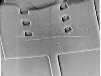
27 POLY DIAPHRAGM PRESSURE SENSOR TEST RESULTS Pressure No Pressure An Pham 1999 Page 27


28 POLY DIAPHARGM PRESSURE SENSOR PACKAGING 500 µm Page 28


29 SECOND VERSION COMPLETED DEVICES - RIT W3 W1 L1 L2 W2 W1 = 300 µm W2 = 1100 W3 = 450 L1 = 1400 L2 = µm Page µm


30 4 TH VERSION CMOS Compatible Tiny Pressure Sensor Page 30

31 4 TH VERSION CMOS Compatible Tiny Pressure Sensor Poly is sacrifical layer, XeF2 Oxide under metal is diaphragm Metal gate Page 31
32 IMPROVED MEMS PRESSURE SENSOR The moving gate MOSFET pressure sensor shows promise for meeting the specifications of small size, low cost, accuracy and high frequency. The major problem in the work presented above is the final packaging and shaping of the probe tip. Devices made on silicon-on-insulator (SOI) could be shaped (in batch mode) by an etching technique. This would give sensors of less than 2µm by 2µm as illustrated below. Page 32


33 BLOOD FLOW Photodiode Strain Sensor Page 33
34 MEMS FLOW SENSORS Heater Flow Spring 2003 EMCR 890 Class Project Upstream Temp Sensor Polysilicon Si3N4 SacOx Silicon Substrate Downstream Temp Sensor Aluminum Page 34
35 REFERENCES 1. Transonic Systems Inc., Tel: (USA); Fax ; Page 35
MEMS Capacitor Sensor Laboratory
 ROCHESTER INSTITUTE OF TEHNOLOGY MICROELECTRONIC ENGINEERING MEMS Capacitor Sensor Laboratory Dr. Lynn Fuller, Dr. Ivan Puchades Webpage: http://people.rit.edu/lffeee 82 Lomb Memorial Drive Rochester,
Evaluation of Pressure Sensor Performance Dr. Lynn Fuller Webpage:
 ROCHESTER INSTITUTE OF TECHNOLOGY MICROELECTRONIC ENGINEERING Evaluation of Pressure Sensor Performance Webpage: http://people.rit.edu/lffeee 82 Lomb Memorial Drive Rochester, NY 14623-5604 Tel (585) 475-2035
MEMS Capacitor Sensors and Signal Conditioning
 ROCHESTER INSTITUTE OF TEHNOLOGY MICROELECTRONIC ENGINEERING MEMS Capacitor Sensors and Signal Conditioning Dr. Lynn Fuller Dr. FullersWebpage: http://people.rit.edu/lffeee Electrical and 82 Lomb Memorial
Surface Analysis. Dr. Lynn Fuller Dr. Fuller s Webpage:
 ROCHESTER INSTITUTE OF TECHNOLOGY MICROELECTRONIC ENGINEERING Surface Analysis Dr. Lynn Fuller Dr. Fuller s Webpage: http://people.rit.edu/lffeee 82 Lomb Memorial Drive Rochester, NY 14623-5604 Tel (585)
Evaluation of Pressure Sensor Performance Dr. Lynn Fuller
 ROCHESTER INSTITUTE OF TECHNOLOGY MICROELECTRONIC ENGINEERING Evaluation of Pressure Sensor Performance Dr. Lynn Fuller Webpage: http://people.rit.edu/lffeee 82 Lomb Memorial Drive Rochester, NY 14623-5604
LAYOUT TECHNIQUES. Dr. Ivan Grech
 LAYOUT TECHNIQUES OUTLINE Transistor Layout Resistor Layout Capacitor Layout Floor planning Mixed A/D Layout Automatic Analog Layout Layout Techniques Main Layers in a typical Double-Poly, Double-Metal
P. R. Nelson 1 ECE418 - VLSI. Midterm Exam. Solutions
 P. R. Nelson 1 ECE418 - VLSI Midterm Exam Solutions 1. (8 points) Draw the cross-section view for A-A. The cross-section view is as shown below.. ( points) Can you tell which of the metal1 regions is the
Spiral 2 7. Capacitance, Delay and Sizing. Mark Redekopp
 2-7.1 Spiral 2 7 Capacitance, Delay and Sizing Mark Redekopp 2-7.2 Learning Outcomes I understand the sources of capacitance in CMOS circuits I understand how delay scales with resistance, capacitance
Lecture 0: Introduction
 Lecture 0: Introduction Introduction q Integrated circuits: many transistors on one chip q Very Large Scale Integration (VLSI): bucketloads! q Complementary Metal Oxide Semiconductor Fast, cheap, low power
Digital Integrated Circuits A Design Perspective
 Semiconductor Memories Adapted from Chapter 12 of Digital Integrated Circuits A Design Perspective Jan M. Rabaey et al. Copyright 2003 Prentice Hall/Pearson Outline Memory Classification Memory Architectures
Pressure Sensor Evaluation Dr. Lynn Fuller Lianna Dicke Webpage:
 ROCHESTER INSTITUTE OF TECHNOLOGY MICROELECTRONIC ENGINEERING Pressure Sensor Evaluation Lianna Dicke Webpage: http://people.rit.edu/lffeee 82 Lomb Memorial Drive Rochester, NY 14623-5604 Email: Lynn.Fuller@rit.edu
EE141- Fall 2002 Lecture 27. Memory EE141. Announcements. We finished all the labs No homework this week Projects are due next Tuesday 9am EE141
 - Fall 2002 Lecture 27 Memory Announcements We finished all the labs No homework this week Projects are due next Tuesday 9am 1 Today s Lecture Memory:» SRAM» DRAM» Flash Memory 2 Floating-gate transistor
MEMS Tuning-Fork Gyroscope Mid-Term Report Amanda Bristow Travis Barton Stephen Nary
 MEMS Tuning-Fork Gyroscope Mid-Term Report Amanda Bristow Travis Barton Stephen Nary Abstract MEMS based gyroscopes have gained in popularity for use as rotation rate sensors in commercial products like
ELEN0037 Microelectronic IC Design. Prof. Dr. Michael Kraft
 ELEN0037 Microelectronic IC Design Prof. Dr. Michael Kraft Lecture 2: Technological Aspects Technology Passive components Active components CMOS Process Basic Layout Scaling CMOS Technology Integrated
VLSI GATE LEVEL DESIGN UNIT - III P.VIDYA SAGAR ( ASSOCIATE PROFESSOR) Department of Electronics and Communication Engineering, VBIT
 Department of Electronics and Communication Engineering, VBIT") VLSI UNIT - III GATE LEVEL DESIGN P.VIDYA SAGAR ( ASSOCIATE PROFESSOR) contents GATE LEVEL DESIGN : Logic Gates and Other complex gates, Switch logic, Alternate gate circuits, Time Delays, Driving large
VLSI UNIT - III GATE LEVEL DESIGN P.VIDYA SAGAR ( ASSOCIATE PROFESSOR) contents GATE LEVEL DESIGN : Logic Gates and Other complex gates, Switch logic, Alternate gate circuits, Time Delays, Driving large
EE115C Winter 2017 Digital Electronic Circuits. Lecture 3: MOS RC Model, CMOS Manufacturing
 EE115C Winter 2017 Digital Electronic Circuits Lecture 3: MOS RC Model, CMOS Manufacturing Agenda MOS Transistor: RC Model (pp. 104-113) S R on D CMOS Manufacturing Process (pp. 36-46) S S C GS G G C GD
Impact-Tek, LLC, Oil Sensors Phase 2, Design Review
 ROCHESTER INSTITUTE OF TECHNOLOGY MICROELECTRONIC ENGINEERING Impact-Tek, LLC, Oil Sensors Phase 2, Design Review Dr. Lynn Fuller Ivan Puchades Webpage: http://people.rit.edu/lffeee 82 Lomb Memorial Drive
UNIVERSITY OF CALIFORNIA College of Engineering Department of Electrical Engineering and Computer Sciences. Professor Oldham Fall 1999
 UNIVERSITY OF CLIFORNI College of Engineering Department of Electrical Engineering and Computer Sciences Professor Oldham Fall 1999 EECS 40 FINL EXM 13 December 1999 Name: Last, First Student ID: T: Kusuma
Low Power CMOS Dr. Lynn Fuller Webpage:
 ROCHESTER INSTITUTE OF TECHNOLOGY MICROELECTRONIC ENGINEERING Dr. Lynn Fuller Webpage: http://people.rit.edu/lffeee 82 Lomb Memorial Drive Rochester, NY 14623-5604 Email: Lynn.Fuller@rit.edu Department
Hw 6 and 7 Graded and available Project Phase 2 Graded Project Phase 3 Launch Today
 EECS141 1 Hw 8 Posted Last one to be graded Due Friday April 30 Hw 6 and 7 Graded and available Project Phase 2 Graded Project Phase 3 Launch Today EECS141 2 1 6 5 4 3 2 1 0 1.5 2 2.5 3 3.5 4 Frequency
VLSI VLSI CIRCUIT DESIGN PROCESSES P.VIDYA SAGAR ( ASSOCIATE PROFESSOR) Department of Electronics and Communication Engineering, VBIT
 Department of Electronics and Communication Engineering, VBIT") VLSI VLSI CIRCUIT DESIGN PROCESSES P.VIDYA SAGAR ( ASSOCIATE PROFESSOR) SYLLABUS UNIT II VLSI CIRCUIT DESIGN PROCESSES: VLSI Design Flow, MOS Layers, Stick Diagrams, Design Rules and Layout, 2 m CMOS Design
VLSI VLSI CIRCUIT DESIGN PROCESSES P.VIDYA SAGAR ( ASSOCIATE PROFESSOR) SYLLABUS UNIT II VLSI CIRCUIT DESIGN PROCESSES: VLSI Design Flow, MOS Layers, Stick Diagrams, Design Rules and Layout, 2 m CMOS Design
SEMICONDUCTOR MEMORIES
 SEMICONDUCTOR MEMORIES Semiconductor Memory Classification RWM NVRWM ROM Random Access Non-Random Access EPROM E 2 PROM Mask-Programmed Programmable (PROM) SRAM FIFO FLASH DRAM LIFO Shift Register CAM
Micro Spectro Photometer ROCHESTER INSTITUTE OF TECHNOLOGY MICROELECTRONIC ENGINEERING. Dr. Lynn Fuller. Webpage:
 ROCHESTER INSTITUTE OF TECHNOLOGY MICROELECTRONIC ENGINEERING Micro Spectro Photometer Dr. Lynn Fuller Webpage: http://people.rit.edu/lffeee 82 Lomb Memorial Drive Rochester, NY 146235604 Tel (585) 4752035
Fig. 1 CMOS Transistor Circuits (a) Inverter Out = NOT In, (b) NOR-gate C = NOT (A or B)
 Inverter Out = NOT In, (b) NOR-gate C = NOT (A or B)") 1 Introduction to Transistor-Level Logic Circuits 1 By Prawat Nagvajara At the transistor level of logic circuits, transistors operate as switches with the logic variables controlling the open or closed
1 Introduction to Transistor-Level Logic Circuits 1 By Prawat Nagvajara At the transistor level of logic circuits, transistors operate as switches with the logic variables controlling the open or closed
Lecture 4: CMOS Transistor Theory
 Introduction to CMOS VLSI Design Lecture 4: CMOS Transistor Theory David Harris, Harvey Mudd College Kartik Mohanram and Steven Levitan University of Pittsburgh Outline q Introduction q MOS Capacitor q
CMOS Digital Integrated Circuits Lec 13 Semiconductor Memories
 Lec 13 Semiconductor Memories 1 Semiconductor Memory Types Semiconductor Memories Read/Write (R/W) Memory or Random Access Memory (RAM) Read-Only Memory (ROM) Dynamic RAM (DRAM) Static RAM (SRAM) 1. Mask
Lecture 210 Physical Aspects of ICs (12/15/01) Page 210-1
 Page 210-1") Lecture 210 Physical Aspects of ICs (12/15/01) Page 210-1 LECTURE 210 PHYSICAL ASPECTS OF ICs (READING: Text-Sec. 2.5, 2.6, 2.8) INTRODUCTION Objective Illustrate the physical aspects of integrated circuits
Lecture 210 Physical Aspects of ICs (12/15/01) Page 210-1 LECTURE 210 PHYSICAL ASPECTS OF ICs (READING: Text-Sec. 2.5, 2.6, 2.8) INTRODUCTION Objective Illustrate the physical aspects of integrated circuits
Microelectromechanical Systems (MEMs) Applications Fluids
 Applications Fluids") ROCHESTER INSTITUTE OF TEHNOLOGY MICROELECTRONIC ENGINEERING Microelectromechanical Systems (MEMs) Applications Fluids Dr. Lynn Fuller Webpage: http://people.rit.edu/lffeee 82 Lomb Memorial Drive Rochester,
ROCHESTER INSTITUTE OF TEHNOLOGY MICROELECTRONIC ENGINEERING Microelectromechanical Systems (MEMs) Applications Fluids Dr. Lynn Fuller Webpage: http://people.rit.edu/lffeee 82 Lomb Memorial Drive Rochester,
EE141- Spring 2003 Lecture 3. Last Lecture
 - Spring 003 Lecture 3 IC Manufacturing 1 Last Lecture Design Metrics (part 1) Today Design metrics (wrap-up) IC manufacturing 1 Administrivia Discussion sessions start this week. Only one this week (Dejan
S No. Questions Bloom s Taxonomy Level UNIT-I
 GROUP-A (SHORT ANSWER QUESTIONS) S No. Questions Bloom s UNIT-I 1 Define oxidation & Classify different types of oxidation Remember 1 2 Explain about Ion implantation Understand 1 3 Describe lithography
Lecture 12: MOS Capacitors, transistors. Context
 Lecture 12: MOS Capacitors, transistors Context In the last lecture, we discussed PN diodes, and the depletion layer into semiconductor surfaces. Small signal models In this lecture, we will apply those
CMOS Inverter. Performance Scaling
 Announcements Exam #2 regrade requests due today. Homework #8 due today. Final Exam: Th June 12, 8:30 10:20am, CMU 120 (extension to 11:20am requested). Grades available for viewing via Catalyst. CMOS
Transfer Gate and Dynamic Logic Dr. Lynn Fuller Webpage:
 ROCHESTER INSTITUTE OF TECHNOLOGY MICROELECTRONIC ENGINEERING Transfer Gate and Dynamic Logic Dr. Lynn Fuller Webpage: http://people.rit.edu/lffeee 82 Lomb Memorial Drive Rochester, NY 14623-5604 Tel (585)
INTEGRATED CIRCUITS. For a complete data sheet, please also download:
 INTEGRATED CIRCUITS DATA SHEET For a complete data sheet, please also download: The IC06 74HC/HCT/HCU/HCMOS Logic Family Specifications The IC06 74HC/HCT/HCU/HCMOS Logic Package Information The IC06 74HC/HCT/HCU/HCMOS
Thin Film Transistors (TFT)
") Thin Film Transistors (TFT) a-si TFT - α-si:h (Hydrogenated amorphous Si) deposited with a PECVD system (low temp. process) replaces the single crystal Si substrate. - Inverted staggered structure with
Thin Film Transistors (TFT) a-si TFT - α-si:h (Hydrogenated amorphous Si) deposited with a PECVD system (low temp. process) replaces the single crystal Si substrate. - Inverted staggered structure with
Lecture 25. Semiconductor Memories. Issues in Memory
 Lecture 25 Semiconductor Memories Issues in Memory Memory Classification Memory Architectures TheMemoryCore Periphery 1 Semiconductor Memory Classification RWM NVRWM ROM Random Access Non-Random Access
Combinatorial and Sequential CMOS Circuits Dr. Lynn Fuller Webpage:
 ROCHESTER INSTITUTE OF TECHNOLOGY MICROELECTRONIC ENGINEERING Combinatorial and Sequential CMOS Circuits Webpage: http://people.rit.edu/lffeee 82 Lomb Memorial Drive Rochester, NY 14623-5604 Tel (585)
EE C245 / ME C218 INTRODUCTION TO MEMS DESIGN FALL 2009 PROBLEM SET #7. Due (at 7 p.m.): Thursday, Dec. 10, 2009, in the EE C245 HW box in 240 Cory.
: Thursday, Dec. 10, 2009, in the EE C245 HW box in 240 Cory.") Issued: Thursday, Nov. 24, 2009 PROBLEM SET #7 Due (at 7 p.m.): Thursday, Dec. 10, 2009, in the EE C245 HW box in 240 Cory. 1. Gyroscopes are inertial sensors that measure rotation rate, which is an extremely
Issued: Thursday, Nov. 24, 2009 PROBLEM SET #7 Due (at 7 p.m.): Thursday, Dec. 10, 2009, in the EE C245 HW box in 240 Cory. 1. Gyroscopes are inertial sensors that measure rotation rate, which is an extremely
Semiconductor Memories
 Semiconductor References: Adapted from: Digital Integrated Circuits: A Design Perspective, J. Rabaey UCB Principles of CMOS VLSI Design: A Systems Perspective, 2nd Ed., N. H. E. Weste and K. Eshraghian
GMU, ECE 680 Physical VLSI Design 1
 ECE680: Physical VLSI Design Chapter VIII Semiconductor Memory (chapter 12 in textbook) 1 Chapter Overview Memory Classification Memory Architectures The Memory Core Periphery Reliability Case Studies
Digital Integrated Circuits A Design Perspective. Semiconductor. Memories. Memories
 Digital Integrated Circuits A Design Perspective Semiconductor Chapter Overview Memory Classification Memory Architectures The Memory Core Periphery Reliability Case Studies Semiconductor Memory Classification
Switched-Capacitor Circuits David Johns and Ken Martin University of Toronto
 Switched-Capacitor Circuits David Johns and Ken Martin University of Toronto (johns@eecg.toronto.edu) (martin@eecg.toronto.edu) University of Toronto 1 of 60 Basic Building Blocks Opamps Ideal opamps usually
Device 3D. 3D Device Simulator. Nano Scale Devices. Fin FET
 Device 3D 3D Device Simulator Device 3D is a physics based 3D device simulator for any device type and includes material properties for the commonly used semiconductor materials in use today. The physical
MEMS Mechanical Fundamentals
 ROCHESTER INSTITUTE OF TECHNOLOGY MICROELECTRONIC ENGINEERING MEMS Mechanical Fundamentals Dr. Lynn Fuller webpage: http://people.rit.edu/lffeee Electrical and Microelectronic Engineering Rochester Institute
EE115C Digital Electronic Circuits Homework #6
 Problem 1 Sizing of adder blocks Electrical Engineering Department Spring 2010 EE115C Digital Electronic Circuits Homework #6 Solution Figure 1: Mirror adder. Study the mirror adder cell (textbook, pages
INSTRUMENTATION ECE Fourth Semester. Presented By:- Sumit Grover Lect., Deptt. of ECE
 INSTRUMENTATION ECE Fourth Semester Presented By:- Sumit Grover Lect., Deptt. of ECE Detailed Contents Objectives Sensors and transducer Classification of transducers Temperature transducers Resistance
ECE520 VLSI Design. Lecture 23: SRAM & DRAM Memories. Payman Zarkesh-Ha
 ECE520 VLSI Design Lecture 23: SRAM & DRAM Memories Payman Zarkesh-Ha Office: ECE Bldg. 230B Office hours: Wednesday 2:00-3:00PM or by appointment E-mail: pzarkesh@unm.edu Slide: 1 Review of Last Lecture
Chapter 2 CMOS Transistor Theory. Jin-Fu Li Department of Electrical Engineering National Central University Jungli, Taiwan
 Chapter 2 CMOS Transistor Theory Jin-Fu Li Department of Electrical Engineering National Central University Jungli, Taiwan Outline Introduction MOS Device Design Equation Pass Transistor Jin-Fu Li, EE,
Chapter 9. Estimating circuit speed. 9.1 Counting gate delays
 Chapter 9 Estimating circuit speed 9.1 Counting gate delays The simplest method for estimating the speed of a VLSI circuit is to count the number of VLSI logic gates that the input signals must propagate
Lecture 21: Packaging, Power, & Clock
 Lecture 21: Packaging, Power, & Clock Outline Packaging Power Distribution Clock Distribution 2 Packages Package functions Electrical connection of signals and power from chip to board Little delay or
VLSI. Faculty. Srikanth
 J.B. Institute of Engineering & Technology Department of CSE COURSE FILE VLSI Faculty Srikanth J.B. Institute of Engineering & Technology Department of CSE SYLLABUS Subject Name: VLSI Subject Code: VLSI
Gold Nanoparticles Floating Gate MISFET for Non-Volatile Memory Applications
 Gold Nanoparticles Floating Gate MISFET for Non-Volatile Memory Applications D. Tsoukalas, S. Kolliopoulou, P. Dimitrakis, P. Normand Institute of Microelectronics, NCSR Demokritos, Athens, Greece S. Paul,
MOSFET: Introduction
 E&CE 437 Integrated VLSI Systems MOS Transistor 1 of 30 MOSFET: Introduction Metal oxide semiconductor field effect transistor (MOSFET) or MOS is widely used for implementing digital designs Its major
Interconnects. Wire Resistance Wire Capacitance Wire RC Delay Crosstalk Wire Engineering Repeaters. ECE 261 James Morizio 1
 Interconnects Wire Resistance Wire Capacitance Wire RC Delay Crosstalk Wire Engineering Repeaters ECE 261 James Morizio 1 Introduction Chips are mostly made of wires called interconnect In stick diagram,
Floating Point Representation and Digital Logic. Lecture 11 CS301
 Floating Point Representation and Digital Logic Lecture 11 CS301 Administrative Daily Review of today s lecture w Due tomorrow (10/4) at 8am Lab #3 due Friday (9/7) 1:29pm HW #5 assigned w Due Monday 10/8
Semiconductor memories
 Semiconductor memories Semiconductor Memories Data in Write Memory cell Read Data out Some design issues : How many cells? Function? Power consuption? Access type? How fast are read/write operations? Semiconductor
CARNEGIE MELLON UNIVERSITY DEPARTMENT OF ELECTRICAL AND COMPUTER ENGINEERING DIGITAL INTEGRATED CIRCUITS FALL 2002
 CARNEGIE MELLON UNIVERSITY DEPARTMENT OF ELECTRICAL AND COMPUTER ENGINEERING 18-322 DIGITAL INTEGRATED CIRCUITS FALL 2002 Final Examination, Monday Dec. 16, 2002 NAME: SECTION: Time: 180 minutes Closed
MOS Transistor Theory
 CHAPTER 3 MOS Transistor Theory Outline 2 1. Introduction 2. Ideal I-V Characteristics 3. Nonideal I-V Effects 4. C-V Characteristics 5. DC Transfer Characteristics 6. Switch-level RC Delay Models MOS
EE 434 Lecture 12. Process Flow (wrap up) Device Modeling in Semiconductor Processes
 Device Modeling in Semiconductor Processes") EE 434 Lecture 12 Process Flow (wrap up) Device Modeling in Semiconductor Processes Quiz 6 How have process engineers configured a process to assure that the thickness of the gate oxide for the p-channel
EE 434 Lecture 12 Process Flow (wrap up) Device Modeling in Semiconductor Processes Quiz 6 How have process engineers configured a process to assure that the thickness of the gate oxide for the p-channel
KINGS COLLEGE OF ENGINEERING DEPARTMENT OF ELECTRONICS AND COMMUNICATION ENGINEERING QUESTION BANK
 KINGS COLLEGE OF ENGINEERING DEPARTMENT OF ELECTRONICS AND COMMUNICATION ENGINEERING QUESTION BANK SUBJECT CODE: EC 1354 SUB.NAME : VLSI DESIGN YEAR / SEMESTER: III / VI UNIT I MOS TRANSISTOR THEORY AND
Topics to be Covered. capacitance inductance transmission lines
 Topics to be Covered Circuit Elements Switching Characteristics Power Dissipation Conductor Sizes Charge Sharing Design Margins Yield resistance capacitance inductance transmission lines Resistance of
Cut-and-Paste Organic FET Customized ICs for Application to Artificial Skin
 Cut-and-Paste Organic FET Customized ICs for Application to Artificial Skin Takao Someya 1, Hiroshi Kawaguchi 2, Takayasu Sakurai 3 1 School of Engineering, University of Tokyo, Tokyo, JAPAN 2 Institute
THE INVERTER. Inverter
 THE INVERTER DIGITAL GATES Fundamental Parameters Functionality Reliability, Robustness Area Performance» Speed (delay)» Power Consumption» Energy Noise in Digital Integrated Circuits v(t) V DD i(t) (a)
Lecture 12 CMOS Delay & Transient Response
 EE 471: Transport Phenomena in Solid State Devices Spring 2018 Lecture 12 CMOS Delay & Transient Response Bryan Ackland Department of Electrical and Computer Engineering Stevens Institute of Technology
MOSIS REPORT. Spring MOSIS Report 1. MOSIS Report 2. MOSIS Report 3
 MOSIS REPORT Spring 2010 MOSIS Report 1 MOSIS Report 2 MOSIS Report 3 MOSIS Report 1 Design of 4-bit counter using J-K flip flop I. Objective The purpose of this project is to design one 4-bit counter
Digital Integrated Circuits
 Chapter 6 The CMOS Inverter 1 Contents Introduction (MOST models) 0, 1 st, 2 nd order The CMOS inverter : The static behavior: o DC transfer characteristics, o Short-circuit current The CMOS inverter :
An Autonomous Nonvolatile Memory Latch
 Radiant Technologies, Inc. 2835D Pan American Freeway NE Albuquerque, NM 87107 Tel: 505-842-8007 Fax: 505-842-0366 e-mail: radiant@ferrodevices.com www.ferrodevices.com An Autonomous Nonvolatile Memory
Digital Integrated Circuits. The Wire * Fuyuzhuo. *Thanks for Dr.Guoyong.SHI for his slides contributed for the talk. Digital IC.
 Digital Integrated Circuits The Wire * Fuyuzhuo *Thanks for Dr.Guoyong.SHI for his slides contributed for the talk Introduction The Wire transmitters receivers schematics physical 2 Interconnect Impact
an introduction to Semiconductor Devices
 an introduction to Semiconductor Devices Donald A. Neamen Chapter 6 Fundamentals of the Metal-Oxide-Semiconductor Field-Effect Transistor Introduction: Chapter 6 1. MOSFET Structure 2. MOS Capacitor -
L ECE 4211 UConn F. Jain Scaling Laws for NanoFETs Chapter 10 Logic Gate Scaling
 L13 04202017 ECE 4211 UConn F. Jain Scaling Laws for NanoFETs Chapter 10 Logic Gate Scaling Scaling laws: Generalized scaling (GS) p. 610 Design steps p.613 Nanotransistor issues (page 626) Degradation
Slide 1. Temperatures Light (Optoelectronics) Magnetic Fields Strain Pressure Displacement and Rotation Acceleration Electronic Sensors
 Magnetic Fields Strain Pressure Displacement and Rotation Acceleration Electronic Sensors") Slide 1 Electronic Sensors Electronic sensors can be designed to detect a variety of quantitative aspects of a given physical system. Such quantities include: Temperatures Light (Optoelectronics) Magnetic
Slide 1 Electronic Sensors Electronic sensors can be designed to detect a variety of quantitative aspects of a given physical system. Such quantities include: Temperatures Light (Optoelectronics) Magnetic
EE 5211 Analog Integrated Circuit Design. Hua Tang Fall 2012
 EE 5211 Analog Integrated Circuit Design Hua Tang Fall 2012 Today s topic: 1. Introduction to Analog IC 2. IC Manufacturing (Chapter 2) Introduction What is Integrated Circuit (IC) vs discrete circuits?
2. (2pts) What is the major difference between an epitaxial layer and a polysilicon layer?
 What is the major difference between an epitaxial layer and a polysilicon layer?") EE 330 Exam 1 Spring 2017 Name Instructions: Students may bring 1 page of notes (front and back) to this exam and a calculator but the use of any device that has wireless communication capability is prohibited.
EE 330 Exam 1 Spring 2017 Name Instructions: Students may bring 1 page of notes (front and back) to this exam and a calculator but the use of any device that has wireless communication capability is prohibited.
AN-1301 APPLICATION NOTE
 AN-131 APPLICATION NOTE One Technology Way P.O. Box 916 Norwood, MA 262-916, U.S.A. Tel: 781.329.47 Fax: 781.461.3113 www.analog.com Using CDCs to Control Motion for Sample Aspiration by Jim Scarlett INTRODUCTION
Self-study problems and questions Processing and Device Technology, FFF110/FYSD13
 Self-study problems and questions Processing and Device Technology, FFF110/FYSD13 Version 2016_01 In addition to the problems discussed at the seminars and at the lectures, you can use this set of problems
Topics. Dynamic CMOS Sequential Design Memory and Control. John A. Chandy Dept. of Electrical and Computer Engineering University of Connecticut
 Topics Dynamic CMOS Sequential Design Memory and Control Dynamic CMOS In static circuits at every point in time (except when switching) the output is connected to either GND or V DD via a low resistance
Too many answers to list.
 ECE/ME 9 Spring 08, Prof. Feinerman, Test # solutions 5/6/08, Closed Book and Closed Notes Undergraduates x 8.5, σ 1.0, Graduates x 78.5, σ 1. Element Molecular weight, grams Atomic number Density, gm/cc
PARALLEL DIGITAL-ANALOG CONVERTERS
 CMOS Analog IC Design Page 10.2-1 10.2 - PARALLEL DIGITAL-ANALOG CONVERTERS CLASSIFICATION OF DIGITAL-ANALOG CONVERTERS CMOS Analog IC Design Page 10.2-2 CURRENT SCALING DIGITAL-ANALOG CONVERTERS GENERAL
Fundamentals of the Metal Oxide Semiconductor Field-Effect Transistor
 Triode Working FET Fundamentals of the Metal Oxide Semiconductor Field-Effect Transistor The characteristics of energy bands as a function of applied voltage. Surface inversion. The expression for the
AE74 VLSI DESIGN JUN 2015
 Q.2 a. Write down the different levels of integration of IC industry. (4) b. With neat sketch explain briefly PMOS & NMOS enhancement mode transistor. N-MOS enhancement mode transistor:- This transistor
nmos IC Design Report Module: EEE 112
 nmos IC Design Report Author: 1302509 Zhao Ruimin Module: EEE 112 Lecturer: Date: Dr.Zhao Ce Zhou June/5/2015 Abstract This lab intended to train the experimental skills of the layout designing of the
M 3 System for Viscous Drag Reduction
 122 Chapter 5 M 3 System for Viscous Drag Reduction In aerospace engineering, drag reduction is one of the most challenging problems of aircraft. Drag limits the maximum speed, the maximum range of flight
Simple piezoresistive accelerometer
 Simple piezoresistive pressure sensor Simple piezoresistive accelerometer Simple capacitive accelerometer Cap wafer C(x)=C(x(a)) Cap wafer may be micromachined silicon, pyrex, Serves as over-range protection,
Chapter 3 Basics Semiconductor Devices and Processing
 Chapter 3 Basics Semiconductor Devices and Processing Hong Xiao, Ph. D. www2.austin.cc.tx.us/hongxiao/book.htm Hong Xiao, Ph. D. www2.austin.cc.tx.us/hongxiao/book.htm 1 Objectives Identify at least two
By-Pass. This voltage is proportional to the liquid level (threewire potentiometer circuit). The resistance reading can
. The resistance reading can") " " ' " ' / The magnetic field which is in the ball or cylindrical floats actuates very small reed contacts through the wall of a guide tube and these pick up an uninterrupted measuring-circuit voltage
" " ' " ' / The magnetic field which is in the ball or cylindrical floats actuates very small reed contacts through the wall of a guide tube and these pick up an uninterrupted measuring-circuit voltage
Variable Capacitance Accelerometers: Design and Applications
 Variable Capacitance Accelerometers: Design and Applications Micromachined silicon variable-capacitance accelerometers are designed for easy manufacture and demanding applications. Tom Connolly, Endevco
MOS Transistor Theory
 MOS Transistor Theory So far, we have viewed a MOS transistor as an ideal switch (digital operation) Reality: less than ideal EE 261 Krish Chakrabarty 1 Introduction So far, we have treated transistors
Interconnects. Introduction
 Interconnects Wire Resistance Wire Capacitance Wire RC Delay Crosstalk Wire Engineering Repeaters ECE 261 Krish Chakrabarty 1 Introduction Chips are mostly made of ires called interconnect In stick diagram,
Analog Integrated Circuit Design Prof. Nagendra Krishnapura Department of Electrical Engineering Indian Institute of Technology, Madras
 Analog Integrated Circuit Design Prof. Nagendra Krishnapura Department of Electrical Engineering Indian Institute of Technology, Madras Lecture No - 42 Fully Differential Single Stage Opamp Hello and welcome
CS 152 Computer Architecture and Engineering
 CS 152 Computer Architecture and Engineering Lecture 12 VLSI II 2005-2-24 John Lazzaro (www.cs.berkeley.edu/~lazzaro) TAs: Ted Hong and David Marquardt www-inst.eecs.berkeley.edu/~cs152/ Last Time: Device
Chapter 4 Field-Effect Transistors
 Chapter 4 Field-Effect Transistors Microelectronic Circuit Design Richard C. Jaeger Travis N. Blalock 5/5/11 Chap 4-1 Chapter Goals Describe operation of MOSFETs. Define FET characteristics in operation
Institute for Electron Microscopy and Nanoanalysis Graz Centre for Electron Microscopy
 Institute for Electron Microscopy and Nanoanalysis Graz Centre for Electron Microscopy Micromechanics Ass.Prof. Priv.-Doz. DI Dr. Harald Plank a,b a Institute of Electron Microscopy and Nanoanalysis, Graz
The Wire EE141. Microelettronica
 The Wire 1 Interconnect Impact on Chip 2 Example: a Bus Network transmitters receivers schematics physical 3 Wire Models All-inclusive model Capacitance-only 4 Impact of Interconnect Parasitics Interconnect
Topic 4. The CMOS Inverter
 Topic 4 The CMOS Inverter Peter Cheung Department of Electrical & Electronic Engineering Imperial College London URL: www.ee.ic.ac.uk/pcheung/ E-mail: p.cheung@ic.ac.uk Topic 4-1 Noise in Digital Integrated
CMOS Cross Section. EECS240 Spring Dimensions. Today s Lecture. Why Talk About Passives? EE240 Process
 EECS240 Spring 202 CMOS Cross Section Metal p - substrate p + diffusion Lecture 2: CMOS Technology and Passive Devices Poly n - well n + diffusion Elad Alon Dept. of EECS EECS240 Lecture 2 4 Today s Lecture
CMOS Transistors, Gates, and Wires
 CMOS Transistors, Gates, and Wires Should the hardware abstraction layers make today s lecture irrelevant? pplication R P C W / R W C W / 6.375 Complex Digital Systems Christopher atten February 5, 006
EE382M-14 CMOS Analog Integrated Circuit Design
 EE382M-14 CMOS Analog Integrated Circuit Design Lecture 3, MOS Capacitances, Passive Components, and Layout of Analog Integrated Circuits MOS Capacitances Type of MOS transistor capacitors Depletion capacitance
CMOS Inverter (static view)
") Review: Design Abstraction Levels SYSTEM CMOS Inverter (static view) + MODULE GATE [Adapted from Chapter 5. 5.3 CIRCUIT of G DEVICE Rabaey s Digital Integrated Circuits,, J. Rabaey et al.] S D Review:
Review: Design Abstraction Levels SYSTEM CMOS Inverter (static view) + MODULE GATE [Adapted from Chapter 5. 5.3 CIRCUIT of G DEVICE Rabaey s Digital Integrated Circuits,, J. Rabaey et al.] S D Review:
Final Exam: 11 May 2001, Friday, 10 AM
 Spring 2001 BE 3600 BioInstrumentation Final Exam: 11 May 2001, Friday, 10 AM ACTUALLY ADMINISTERED IN CLASS This exam: Consists of 12 questions, Score from this exam will determine 25-30 % of your grade,
and V DS V GS V T (the saturation region) I DS = k 2 (V GS V T )2 (1+ V DS )
 I DS = k 2 (V GS V T )2 (1+ V DS )") ECE 4420 Spring 2005 Page 1 FINAL EXAMINATION NAME SCORE /100 Problem 1O 2 3 4 5 6 7 Sum Points INSTRUCTIONS: This exam is closed book. You are permitted four sheets of notes (three of which are your sheets
ECE 4420 Spring 2005 Page 1 FINAL EXAMINATION NAME SCORE /100 Problem 1O 2 3 4 5 6 7 Sum Points INSTRUCTIONS: This exam is closed book. You are permitted four sheets of notes (three of which are your sheets