Semiconductor X-Ray Detectors. Tobias Eggert Ketek GmbH
|
|
|
- Wendy Davis
- 6 years ago
- Views:
Transcription

1 Semiconductor X-Ray Detectors Tobias Eggert Ketek GmbH
2 Semiconductor X-Ray Detectors Part A Principles of Semiconductor Detectors 1. Basic Principles 2. Typical Applications 3. Planar Technology 4. Read-out Electronics Part B Silicon Drift Detectors 1. Silicon Drift Detectors 2. GaAs Detectors 3. Outlook 4. Resume
 X-ray astronomy detectors with spatial and energy resolution Fully depleted")
3 Motivation Many discoveries and results of fundamental research are closely related to the quality of the instruments used Telescopes, Microscopes, Cameras New detector concepts enabled the discovery of many elementary particles (e +, ν, J/ψ) X-ray astronomy detectors with spatial and energy resolution Fully depleted pn-ccd

4 Why Semiconductor Detectors? Photons and charged particles ionize matter Gases: electron ion pairs are produced Semiconductors: electron hole pairs are produced Measurement of position and energy Pair creation energy in semiconductors is much lower than ionization energy in gases High density of solids high interaction probability Integration of transistors and read-out electronics
5 Semiconductor Detectors p-i-n configuration depletion zone Al saturation of free bonds contacts p + reflects visible light p + maximum at the surface no dead layer high electric field strength e - -hole pairs generated by radiation charge separated and collected current mode: current prop. to flux and energy single photon counting: signal amplitude prop. to deposited charge Al γ U SiO 2 p + n-si n + Al
6 Semiconductor X-Ray Detectors Part A Principles of Semiconductor Detectors 1. Basic Principles 2. Typical Applications 3. Planar Technology 4. Read-out Electronics Part B Silicon Drift Detectors 1. Silicon Drift Detectors 2. GaAs 3. Outlook 4. Resume
7 Applications in Basic Research High Energy Physics Silicon Strip detectors 20 µm 1 µm Al 0.2 µm SiO µm n - Si (2 kωcm) p + implant n + implant 0.5 µm Al position resolution: pitch / 12 Diode array for position measurement


8 Applications in Basic Research High Energy Physics Strip or pixel detectors as inner trackers position resolution


9 Applications in Basic Research X-Ray Astronomy Spectroscopy of cosmic x-ray sources Fully depleted pn-ccd on ESA s x-ray multi-mirror mission (XMM)
10 X-Ray Fluorescence L K nucleus
11 X-Ray Fluorescence L K nucleus
12 X-Ray Fluorescence L K nucleus
13 X-Ray Fluorescence Energy of fluorescence photon = difference of binding energies Moseleys Law: E F prop. to Z 2 L K nucleus Many transitions possible Transitions into K-shell: K α, β photons ( peaks ) Transitions into L-shell: L α, β,γ, η, L photons Higher fluorescence yield for high Z elements
 Excitation of sample")
14 Application X-Ray Fluorescence Analysis (XRF) Excitation of sample with X-rays
15 Application XRF with scanning electron microscopes Excitation of sample with electrons
16

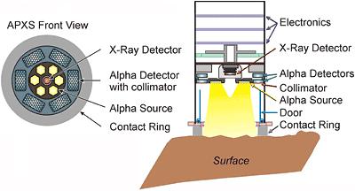
17 NASA Mars Rovers
18 Semiconductor X-Ray Detectors Part A Principles of Semiconductor Detectors 1. Basic Principles 2. Typical Applications 3. Planar Technology 4. Read-out Electronics Part B Silicon Drift Detectors 1. Silicon Drift Detectors 2. GaAs Detectors 3. Outlook 4. Resume
19 Planar Technology Boron Doping by ion implantation and Deposition annealing of at 600 C Opening LPCVD-Nitride N-Si Thermal Metal Wafer deposition of Oxidation of contact windows andholes B: LPCVD-Oxide and 15 kev, patterning at cm 800 C -2 P: 30 kev, cm -2 Phosphorus Differences to conventional planar technology Wafer structured on both sides Larger structures Low temperature processes Less diffusion of impurities Low leakage currents and high charge carrier life-times
20 Planar Technology n-si wafer Deposition of LPCVD-Nitride and LPCVD-Oxide Thermal oxidation Opening of contact holes Opening of windows Boron Metal deposition and patterning Doping by ion implantation and annealing at 600 C B: 15 kev, 5x10 14 cm -2 P: 30 kev, 5x10 15 cm -2 Phosphorus
21 Important Semiconductor Properties atomic number atomic weight density band gap (RT) minority carrier lifetime τ µτ product (e) µτ product (h) intrinsic resistivity intrinsic carrier conc. g/cm 3 ev av. energy for e-h pair ev electron mobility µ e cm 2 /Vs hole mobility µ h cm 2 /Vs s cm 2 /V cm 2 /V Ω cm cm -3 Si Ge GaAs 31 / SiC 14 / >


22 pn-junction for Detector Applications p n diffusion of majority carriers formation of depletion layers ρ A - D + x fixed space charge of acceptors (A - ) and donors (D + ) E x electric field due to space charge E C -E m E F E V q V bi band bending of the junction built in voltage
23 Properties of Si pn-junction Detectors Depletion layer thickness d d/cm = (ρ U/(ΩcmV)) 1/2 ρ U resistivity bias voltage Capacitance C C/pF = A/cm²(ρ U/(ΩcmV)) -1/2 A junction area Al γ -U Reverse current I R I R = I D + I S + I G For thick depletion layers I R = I G = q (n i /τ)a (ρ U) 1/2 I R U 1/2 /τ I D diffusion current I S surface leakage c. I G generation current n i cm -3 intrinsic carrier conc. τ minority carrier lifetime q 1.6x10⁻¹⁹ As SiO 2 p + n-si n + Al
24 The Response of Energy Dispersive X-Ray Detectors Part A Principles of Semiconductor Detectors 1. Basic Principles 2. Typical Applications 3. Planar Technology 4. Read-out Electronics, Spectra, Efficiency Limits Part B Silicon Drift Detectors 1. SDD structure 2. Low Energy Measurements/Experimental Setup 3. Calculation of Spectral Contributions 4. Results 5. Resume
25 Read Out Electronics
26 Requirements on Spectrometers Good energy resolution = narrow peaks High energy range Low background High count-rate ability, large area Radiation hardness
27 Spectrum of Martian Soil Energy resolution of 160 ev FWHM at 5.9 kev
28 Spectrum of Martian Soil Peak width is determined by 1. Ionization statistics (intrinsic) Fano factor 2. Detector leakage currents 3. Electronic noise of read-out electronics
29 Absorption Lengths of Si + Al bulk thickness = 0.28 mm absorption law I(d) = I 0 exp(-d/λ(e)) Al thickness = 100 nm Good efficiency from 250 ev to 11 kev (20 kev)
30 Quantum Efficiency ε = interaction probability Soft X-Rays from 100 ev 30 kev
31 Conventional Radiation Detectors Al γ U SiO 2 p + n-si Main problem of pin diodes and conventional Si(Li)s: Capacitance prop. to area Large active area required for high sensitivity Low capacitance required for low noise The drift principles allows both, large area and low capacitance n + Al
32 The Response of Energy Dispersive X-Ray Detectors Part A Principles of Semiconductor Detectors 1. Basic Principles 2. Typical Applications 3. Planar Technology 4. Read-out Electronics, Spectra, Efficiency Limits Part B Silicon Drift Detectors 1. Silicon Drift Detectors 2. GaAs Detectors 3. Outlook 4. Resume
33 Silicon Drift Detector (SDD) High resistivity, high purity n-type silicon (10 12 /cm 3 ) pn junctions on both sides Drift rings at the front side, integrated voltage dividers Homogeneous entrance window at the back side
34 Silicon Drift Detector (SDD) Depletion from back contact towards bulk contact (n +, not shown) Vertical and lateral drift field small anode size low capacitance Low leakage currents, low noise, high energy resolution Thermoelectrically cooled to 20 C (other detectors need 77 K) Current entrance window: large background for energies < 300 ev
35 Silicon Drift Detector (SDD) Integrated Junction Field Effect Transistor Energy resolution down to 135 ev (FWHM) at 5.9 kev No pickup noise, no microphony, low overall noise Shaping times 250 ns 1 µs (other detectors: 20 µs) Count-rate ability up to 10 6 /s, suited for high X-ray intensities
 front side (drift rings)")
36 Drift Field Configuration back side (radiation entrance window) front side (drift rings) anode

37 History Josef Kemmer develops planar technology for semiconductor detectors 1983 E. Gatti and P. Rehak introduce principle of silicon drift detector 1983 Cooperation between J. Kemmer, P. Rehak and MPI, first SDDs produced at TU München Cooperation with MPI to develop new detector concepts: SDD with homogeneous entrance window, completely depleted pn-ccd for XMM X-ray telescope, DEPMOS, DEPFET 1991 Qualification of Kemmer s planar process for the MPI semiconductor laboratory completed 1998 First commercial SDD systems available th SDD system sold

38 Mounted Devices 5 mm 2, 10 mm 2 7 channel detector with 35 mm 2

39 Mounted Devices Illuminated from back-side Anode continuously discharged no reset clock Standard: 8 µm Be window Polyimide window with Si grid also available N 2 filled housing (1 bar or 100 mbar)
40
41 Si Al
42
43 Semiconductor X-Ray Detectors Part A Principles of Semiconductor Detectors 1. Basic Principles 2. Typical Applications 3. Planar Technology 4. Read-out Electronics Part B Silicon Drift Detectors 1. Silicon Drift Detectors 2. GaAs Detectors 3. Outlook 4. Resume
44 GaAs Detectors Silicon detectors with reasonable thicknesses (< 5 mm) are mainly sensitive to soft X-rays GaAs has higher Z and higher ρ high absorption probability XRF application: detection of X-rays > 30 kev elements have higher fluorescence yield Hard X-rays ( 100 kev) used in medicine: radiography, fluoroscopy, and nuclear medicine Detector with high efficiency reduces dose on patient Band gap of GaAs (1.42 ev) is high enough operation at room temperature operation possible Band gap is low enough for good resolution (Fano limit 140 ev FWHM at 5.9 kev, pair creation energy 4.2 ev) Large bulk resistivity high fields for charge collection Electron mobilities 6 x higher than Si Fast signal
45 Production of GaAs Detectors No natural oxide Production not as easy as in Si planar technology Thickness > 100 µm required for high efficiency detection of hard X-rays and γ -rays and low detector capacitance Not possible with molecular beam epitaxy Maximum thickness with chemical vapor phase deposition epitaxy: µm Most promising: liquid phase technology (Prof. Andreev, Ioffe Institute) Energy resolution of 220 ev obtained with 0.04 mm² 5.9 kev and -30 C Drift principle required to reduce capacitance Very important: high purity epitaxial layer
46 Semiconductor X-Ray Detectors Part A Principles of Semiconductor Detectors 1. Basic Principles 2. Typical Applications 3. Planar Technology 4. Read-out Electronics Part B Silicon Drift Detectors 1. Silicon Drift Detectors 2. GaAs Detectors 3. Outlook 4. Resume
47 Outlook Focus in the past: Silicon drift detectors and read-out electronics spectrometer Competitors: High-end: Si(Li)s, HPGe (for γ ) Low-end: pin-diodes Future Targets: SDDs with larger areas (> 10 mm²) Less charge low at E 0 < 300eV Scintillator-covered SDDs for γ -rays GaAs detectors for hard X-rays (E 0 > 50 kev)
48 The Response of Energy Dispersive X-Ray Detectors Part A Principles of Semiconductor Detectors 1. Basic Principles 2. Typical Applications 3. Planar Technology 4. Read-out Electronics Part B Silicon Drift Detectors 1. Silicon Drift Detectors 2. Low Energy Measurements/Experimental Setup 3. Calculation of Spectral Contributions 4. Results 5. Resume
49 Resume Ketek s Silicon Drift Detector is a unique and established product for XRF and SEM applications Highly optimized production process low leakage currents Drift priciple low capacitance Low overall noise very good energy resolution high count-rate ability Future tasks: Expand energy range to both, higher and lower X-ray energies High E: GaAs detectors Low E: SDD with optimized entrace window /
50 X-ray photon hits detector γ
51 Interaction always by photoelectric effect Compton effect unlikely γ e e + pair creation impossible
52 Creation of one photo electron E = E 0 -E B E 0 > Si K shell: K electron E 0 < Si K shell: L electron γ e pho
53 K or L electron knocked off its shell atom single ionized γ e pho
54 Hole in K or L shell filled with electrons from higher shells. Energy difference assigned to fluorescence photon or Auger electron of fixed energy Fluorescence yields: L shell: 0% K shell: 4% γ e pho e aug
55 Primary photo electron scatters and can generate secondary electrons from Si atoms γ e aug e pho
56 More atoms are ionized and further Auger electrons emerge γ e aug e pho
57 Also possible: Scattering at lattice, i.e. energy carried to phonons Very probable at low energies γ e aug e pho
58 The primary Auger electron also produces secondaries and phonons Number of electrons generated: Ionization/Fano statistics γ e pho e aug
59 K shell fluorescence: X-ray can escape or is reabsorbed inside detector γ γ esc e pho
Semiconductor Detectors
 Semiconductor Detectors Summary of Last Lecture Band structure in Solids: Conduction band Conduction band thermal conductivity: E g > 5 ev Valence band Insulator Charge carrier in conductor: e - Charge
Chem 481 Lecture Material 3/20/09
 Chem 481 Lecture Material 3/20/09 Radiation Detection and Measurement Semiconductor Detectors The electrons in a sample of silicon are each bound to specific silicon atoms (occupy the valence band). If
Advantages / Disadvantages of semiconductor detectors
 Advantages / Disadvantages of semiconductor detectors Semiconductor detectors have a high density (compared to gas detector) large energy loss in a short distance diffusion effect is smaller than in gas
Semiconductor-Detectors
 Semiconductor-Detectors 1 Motivation ~ 195: Discovery that pn-- junctions can be used to detect particles. Semiconductor detectors used for energy measurements ( Germanium) Since ~ 3 years: Semiconductor
Energetic particles and their detection in situ (particle detectors) Part II. George Gloeckler
 Part II. George Gloeckler") Energetic particles and their detection in situ (particle detectors) Part II George Gloeckler University of Michigan, Ann Arbor, MI University of Maryland, College Park, MD Simple particle detectors Gas-filled
Energetic particles and their detection in situ (particle detectors) Part II George Gloeckler University of Michigan, Ann Arbor, MI University of Maryland, College Park, MD Simple particle detectors Gas-filled
EE 5344 Introduction to MEMS CHAPTER 5 Radiation Sensors
 EE 5344 Introduction to MEMS CHAPTER 5 Radiation Sensors 5. Radiation Microsensors Radiation µ-sensors convert incident radiant signals into standard electrical out put signals. Radiant Signals Classification
Radiation Detector 2016/17 (SPA6309)
") Radiation Detector 2016/17 (SPA6309) Semiconductor detectors (Leo, Chapter 10) 2017 Teppei Katori Semiconductor detectors are used in many situations, mostly for some kind of high precision measurement.
Radiation Detector 2016/17 (SPA6309) Semiconductor detectors (Leo, Chapter 10) 2017 Teppei Katori Semiconductor detectors are used in many situations, mostly for some kind of high precision measurement.
Silicon Drift Detectors: Understanding the Advantages for EDS Microanalysis. Patrick Camus, PhD Applications Scientist March 18, 2010
 Silicon Drift Detectors: Understanding the Advantages for EDS Microanalysis Patrick Camus, PhD Applications Scientist March 18, 2010 EDS Detector Requirements Detect whole energy range of x-rays 50 ev
Lecture 2. Introduction to semiconductors Structures and characteristics in semiconductors
 Lecture 2 Introduction to semiconductors Structures and characteristics in semiconductors Semiconductor p-n junction Metal Oxide Silicon structure Semiconductor contact Literature Glen F. Knoll, Radiation
Classification of Solids
 Classification of Solids Classification by conductivity, which is related to the band structure: (Filled bands are shown dark; D(E) = Density of states) Class Electron Density Density of States D(E) Examples
Silicon Detectors in High Energy Physics
 Thomas Bergauer (HEPHY Vienna) IPM Teheran 22 May 2011 Sunday: Schedule Silicon Detectors in Semiconductor Basics (45 ) Detector concepts: Pixels and Strips (45 ) Coffee Break Strip Detector Performance
Lecture 2. Introduction to semiconductors Structures and characteristics in semiconductors
 Lecture 2 Introduction to semiconductors Structures and characteristics in semiconductors Semiconductor p-n junction Metal Oxide Silicon structure Semiconductor contact Literature Glen F. Knoll, Radiation
Lecture 18. New gas detectors Solid state trackers
 Lecture 18 New gas detectors Solid state trackers Time projection Chamber Full 3-D track reconstruction x-y from wires and segmented cathode of MWPC z from drift time de/dx information (extra) Drift over
Analysis of Background Events in Silicon Drift Detectors
 Analysis of Background Events in Silicon Drift Detectors T. Eggert a, P. Goldstrass a J. Kemmer a A. Pahlke b a Ketek GmbH, Gustav-Heinemann-Ring 125, D-81739 München, Germany b MPI Halbleiterlabor, Otto-Hahn-Ring
Chap. 11 Semiconductor Diodes
 Chap. 11 Semiconductor Diodes Semiconductor diodes provide the best resolution for energy measurements, silicon based devices are generally used for charged-particles, germanium for photons. Scintillators
Development of High-Z Semiconductor Detectors and Their Applications to X-ray/gamma-ray Astronomy
 Development of High-Z Semiconductor Detectors and Their Applications to X-ray/gamma-ray Astronomy Taka Tanaka (SLAC/KIPAC) 9/19/2007 SLAC Advanced Instrumentation Seminar Outline Introduction CdTe Diode
Semiconductor Detectors are Ionization Chambers. Detection volume with electric field Energy deposited positive and negative charge pairs
 1 V. Semiconductor Detectors V.1. Principles Semiconductor Detectors are Ionization Chambers Detection volume with electric field Energy deposited positive and negative charge pairs Charges move in field
Spring Semester 2012 Final Exam
 Spring Semester 2012 Final Exam Note: Show your work, underline results, and always show units. Official exam time: 2.0 hours; an extension of at least 1.0 hour will be granted to anyone. Materials parameters
Lecture 2. Introduction to semiconductors Structures and characteristics in semiconductors. Fabrication of semiconductor sensor
 Lecture 2 Introduction to semiconductors Structures and characteristics in semiconductors Semiconductor p-n junction Metal Oxide Silicon structure Semiconductor contact Fabrication of semiconductor sensor
Semiconductor Physics fall 2012 problems
 Semiconductor Physics fall 2012 problems 1. An n-type sample of silicon has a uniform density N D = 10 16 atoms cm -3 of arsenic, and a p-type silicon sample has N A = 10 15 atoms cm -3 of boron. For each
Peter Fischer, ziti, Universität Heidelberg. Silicon Detectors & Readout Electronics
 Silicon Detectors and Readout Electronics Peter Fischer, ziti, Universität Heidelberg 1 Content of the Lecture (sorted by subject) Introduction: Applications of silicon detectors Requirements, measured
Components of a generic collider detector
 Lecture 24 Components of a generic collider detector electrons - ionization + bremsstrahlung photons - pair production in high Z material charged hadrons - ionization + shower of secondary interactions
Review of Semiconductor Drift Detectors
 Pavia October 25, 2004 Review of Semiconductor Drift Detectors Talk given by Pavel Rehak following a presentation on 5 th Hiroshima Symposium of Semiconductor Tracking Detectors Outline of the Review Principles
1 Name: Student number: DEPARTMENT OF PHYSICS AND PHYSICAL OCEANOGRAPHY MEMORIAL UNIVERSITY OF NEWFOUNDLAND. Fall :00-11:00
 1 Name: DEPARTMENT OF PHYSICS AND PHYSICAL OCEANOGRAPHY MEMORIAL UNIVERSITY OF NEWFOUNDLAND Final Exam Physics 3000 December 11, 2012 Fall 2012 9:00-11:00 INSTRUCTIONS: 1. Answer all seven (7) questions.
Introduction to Semiconductor Physics. Prof.P. Ravindran, Department of Physics, Central University of Tamil Nadu, India
 Introduction to Semiconductor Physics 1 Prof.P. Ravindran, Department of Physics, Central University of Tamil Nadu, India http://folk.uio.no/ravi/cmp2013 Review of Semiconductor Physics Semiconductor fundamentals
Engineering 2000 Chapter 8 Semiconductors. ENG2000: R.I. Hornsey Semi: 1
 Engineering 2000 Chapter 8 Semiconductors ENG2000: R.I. Hornsey Semi: 1 Overview We need to know the electrical properties of Si To do this, we must also draw on some of the physical properties and we
Chemical Analysis in TEM: XEDS, EELS and EFTEM. HRTEM PhD course Lecture 5
 Chemical Analysis in TEM: XEDS, EELS and EFTEM HRTEM PhD course Lecture 5 1 Part IV Subject Chapter Prio x-ray spectrometry 32 1 Spectra and mapping 33 2 Qualitative XEDS 34 1 Quantitative XEDS 35.1-35.4
Germanium Detectors. Germanium, a special material. Detectors, big is beautiful. Operational features. Applications. Iris Abt
 Germanium Detectors Germanium, a special material Detectors, big is beautiful Operational features Applications Iris Abt Si Si Si Si Si Si n silicon Si + P The Material Si Donor Si Si conduction valence
SILICON DRIFT DETECTORS FOR HIGH RESOLUTION, HIGH COUNT RATE X-RAY SPECTROSCOPY AT ROOM TEMPERATURE
 Copyright JCPDS - International Centre for Diffraction Data 2004, Advances in X-ray Analysis, Volume 47. 53 SILICON DRIFT DETECTORS FOR HIGH RESOLUTION, HIGH COUNT RATE X-RAY SPECTROSCOPY AT ROOM TEMPERATURE
Chapter 1 Overview of Semiconductor Materials and Physics
 Chapter 1 Overview of Semiconductor Materials and Physics Professor Paul K. Chu Conductivity / Resistivity of Insulators, Semiconductors, and Conductors Semiconductor Elements Period II III IV V VI 2 B
Gamma and X-Ray Detection
 Gamma and X-Ray Detection DETECTOR OVERVIEW The kinds of detectors commonly used can be categorized as: a. Gas-filled Detectors b. Scintillation Detectors c. Semiconductor Detectors The choice of a particular
Lecture 8. Detectors for Ionizing Particles
 Lecture 8 Detectors for Ionizing Particles Content Introduction Overview of detector systems Sources of radiation Radioactive decay Cosmic Radiation Accelerators Interaction of Radiation with Matter General
Semiconductor Detectors
 Radiation Measurement Systems Semiconductor Detectors Ho Kyung Kim Pusan National University Semiconductors Differences btwn semiconductor & gas as a material for radiation detectors Higher (1,000 ) Free
collisions of electrons. In semiconductor, in certain temperature ranges the conductivity increases rapidly by increasing temperature
 1.9. Temperature Dependence of Semiconductor Conductivity Such dependence is one most important in semiconductor. In metals, Conductivity decreases by increasing temperature due to greater frequency of
Detecting high energy photons. Interactions of photons with matter Properties of detectors (with examples)
") Detecting high energy photons Interactions of photons with matter Properties of detectors (with examples) Interactions of high energy photons with matter Cross section/attenution length/optical depth Photoelectric
Detecting high energy photons Interactions of photons with matter Properties of detectors (with examples) Interactions of high energy photons with matter Cross section/attenution length/optical depth Photoelectric
PN Junction
 P Junction 2017-05-04 Definition Power Electronics = semiconductor switches are used Analogue amplifier = high power loss 250 200 u x 150 100 u Udc i 50 0 0 50 100 150 200 250 300 350 400 i,u dc i,u u
Semiconductor Physics Problems 2015
 Semiconductor Physics Problems 2015 Page and figure numbers refer to Semiconductor Devices Physics and Technology, 3rd edition, by SM Sze and M-K Lee 1. The purest semiconductor crystals it is possible
A semiconductor is an almost insulating material, in which by contamination (doping) positive or negative charge carriers can be introduced.
 positive or negative charge carriers can be introduced.") Semiconductor A semiconductor is an almost insulating material, in which by contamination (doping) positive or negative charge carriers can be introduced. Page 2 Semiconductor materials Page 3 Energy levels
Semiconductor A semiconductor is an almost insulating material, in which by contamination (doping) positive or negative charge carriers can be introduced. Page 2 Semiconductor materials Page 3 Energy levels
Solid State Detectors
 Solid State Detectors Most material is taken from lectures by Michael Moll/CERN and Daniela Bortoletto/Purdue and the book Semiconductor Radiation Detectors by Gerhard Lutz. In gaseous detectors, a charged
smal band gap Saturday, April 9, 2011
 small band gap upper (conduction) band empty small gap valence band filled 2s 2p 2s 2p hybrid (s+p)band 2p no gap 2s (depend on the crystallographic orientation) extrinsic semiconductor semi-metal electron
Final Examination EE 130 December 16, 1997 Time allotted: 180 minutes
 Final Examination EE 130 December 16, 1997 Time allotted: 180 minutes Problem 1: Semiconductor Fundamentals [30 points] A uniformly doped silicon sample of length 100µm and cross-sectional area 100µm 2
Solid State Detectors Semiconductor detectors Halbleiterdetektoren
 Solid State Detectors Semiconductor detectors Halbleiterdetektoren Doris Eckstein DESY Where are solid state detectors used? > Nuclear Physics: Energy measurement of charged particles (particles up to
Session 5: Solid State Physics. Charge Mobility Drift Diffusion Recombination-Generation
 Session 5: Solid State Physics Charge Mobility Drift Diffusion Recombination-Generation 1 Outline A B C D E F G H I J 2 Mobile Charge Carriers in Semiconductors Three primary types of carrier action occur
OPTI510R: Photonics. Khanh Kieu College of Optical Sciences, University of Arizona Meinel building R.626
 OPTI510R: Photonics Khanh Kieu College of Optical Sciences, University of Arizona kkieu@optics.arizona.edu Meinel building R.626 Announcements Homework #6 is assigned, due May 1 st Final exam May 8, 10:30-12:30pm
XRF books: Analytical Chemistry, Kellner/Mermet/Otto/etc. 3 rd year XRF Spectroscopy Dr. Alan Ryder (R222, Physical Chemistry) 2 lectures:
 2 lectures:") 1 3 rd year XRF Spectroscopy Dr. Alan Ryder (R222, Physical Chemistry) 2 lectures: XRF spectroscopy 1 exam question. Notes on: www.nuigalway.ie/nanoscale/3rdspectroscopy.html XRF books: Analytical Chemistry,
1 3 rd year XRF Spectroscopy Dr. Alan Ryder (R222, Physical Chemistry) 2 lectures: XRF spectroscopy 1 exam question. Notes on: www.nuigalway.ie/nanoscale/3rdspectroscopy.html XRF books: Analytical Chemistry,
Junction Diodes. Tim Sumner, Imperial College, Rm: 1009, x /18/2006
 Junction Diodes Most elementary solid state junction electronic devices. They conduct in one direction (almost correct). Useful when one converts from AC to DC (rectifier). But today diodes have a wide
Semiconductor Physics fall 2012 problems
 Semiconductor Physics fall 2012 problems 1. An n-type sample of silicon has a uniform density N D = 10 16 atoms cm -3 of arsenic, and a p-type silicon sample has N A = 10 15 atoms cm -3 of boron. For each
Single Photon detectors
 Single Photon detectors Outline Motivation for single photon detection Semiconductor; general knowledge and important background Photon detectors: internal and external photoeffect Properties of semiconductor
Radiation Detection for the Beta- Delayed Alpha and Gamma Decay of 20 Na. Ellen Simmons
 Radiation Detection for the Beta- Delayed Alpha and Gamma Decay of 20 Na Ellen Simmons 1 Contents Introduction Review of the Types of Radiation Charged Particle Radiation Detection Review of Semiconductor
UNIVERSITY OF CALIFORNIA College of Engineering Department of Electrical Engineering and Computer Sciences. Professor Chenming Hu.
 UNIVERSITY OF CALIFORNIA College of Engineering Department of Electrical Engineering and Computer Sciences EECS 130 Spring 2009 Professor Chenming Hu Midterm I Name: Closed book. One sheet of notes is
Section 12: Intro to Devices
 Section 12: Intro to Devices Extensive reading materials on reserve, including Robert F. Pierret, Semiconductor Device Fundamentals Bond Model of Electrons and Holes Si Si Si Si Si Si Si Si Si Silicon
ORTEC. Review of the Physics of Semiconductor Detectors. Interaction of Ionizing Radiation with Semiconductor Detectors. Heavy Charged Particles
 ORTEC Review of the Physics of Historically, semiconductor detectors were conceived as solid-state ionization chambers. To obtain a high-electric-field, low-current, solid-state device for detection and
Theory of Electrical Characterization of Semiconductors
 Theory of Electrical Characterization of Semiconductors P. Stallinga Universidade do Algarve U.C.E.H. A.D.E.E.C. OptoElectronics SELOA Summer School May 2000, Bologna (It) Overview Devices: bulk Schottky
Review of Semiconductor Fundamentals
 ECE 541/ME 541 Microelectronic Fabrication Techniques Review of Semiconductor Fundamentals Zheng Yang (ERF 3017, email: yangzhen@uic.edu) Page 1 Semiconductor A semiconductor is an almost insulating material,
EEE4106Z Radiation Interactions & Detection
 EEE4106Z Radiation Interactions & Detection 2. Radiation Detection Dr. Steve Peterson 5.14 RW James Department of Physics University of Cape Town steve.peterson@uct.ac.za May 06, 2015 EEE4106Z :: Radiation
3.1 Introduction to Semiconductors. Y. Baghzouz ECE Department UNLV
 3.1 Introduction to Semiconductors Y. Baghzouz ECE Department UNLV Introduction In this lecture, we will cover the basic aspects of semiconductor materials, and the physical mechanisms which are at the
Photon Instrumentation. First Mexican Particle Accelerator School Guanajuato Oct 6, 2011
 Photon Instrumentation First Mexican Particle Accelerator School Guanajuato Oct 6, 2011 Outline The Electromagnetic Spectrum Photon Detection Interaction of Photons with Matter Photoelectric Effect Compton
KATIHAL FİZİĞİ MNT-510
 KATIHAL FİZİĞİ MNT-510 YARIİLETKENLER Kaynaklar: Katıhal Fiziği, Prof. Dr. Mustafa Dikici, Seçkin Yayıncılık Katıhal Fiziği, Şakir Aydoğan, Nobel Yayıncılık, Physics for Computer Science Students: With
Lecture 1. OUTLINE Basic Semiconductor Physics. Reading: Chapter 2.1. Semiconductors Intrinsic (undoped) silicon Doping Carrier concentrations
 silicon Doping Carrier concentrations") Lecture 1 OUTLINE Basic Semiconductor Physics Semiconductors Intrinsic (undoped) silicon Doping Carrier concentrations Reading: Chapter 2.1 EE105 Fall 2007 Lecture 1, Slide 1 What is a Semiconductor? Low
Lecture 1 OUTLINE Basic Semiconductor Physics Semiconductors Intrinsic (undoped) silicon Doping Carrier concentrations Reading: Chapter 2.1 EE105 Fall 2007 Lecture 1, Slide 1 What is a Semiconductor? Low
Development and characterization of 3D semiconductor X-rays detectors for medical imaging
 Development and characterization of 3D semiconductor X-rays detectors for medical imaging Marie-Laure Avenel, Eric Gros d Aillon CEA-LETI, DETectors Laboratory marie-laure.avenel@cea.fr Outlines Problematic
Chapter 6: Basic radiation detectors
 Chapter 6: Basic radiation detectors Set of 60 slides based on the chapter authored by C.W.E. VAN EIJK Faculty of Applied Sciences, Delft University of Technology, Delft, Netherlands of the publication
SEM. Chemical Analysis in the. Elastic and Inelastic scattering. Chemical analysis in the SEM. Chemical analysis in the SEM
 THE UNIVERSITY Chemical Analysis in the SEM Ian Jones Centre for Electron Microscopy OF BIRMINGHAM Elastic and Inelastic scattering Electron interacts with one of the orbital electrons Secondary electrons,
Introduction into Positron Annihilation
 Introduction into Positron Annihilation Introduction (How to get positrons? What is special about positron annihilation?) The methods of positron annihilation (positron lifetime, Doppler broadening, ACAR...)
Status Report: Charge Cloud Explosion
 Status Report: Charge Cloud Explosion J. Becker, D. Eckstein, R. Klanner, G. Steinbrück University of Hamburg Detector laboratory 1. Introduction and Motivation. Set-up available for measurement 3. Measurements
electronics fundamentals
 electronics fundamentals circuits, devices, and applications THOMAS L. FLOYD DAVID M. BUCHLA Lesson 1: Diodes and Applications Semiconductors Figure 1-1 The Bohr model of an atom showing electrons in orbits
Lecture 2. Semiconductor Physics. Sunday 4/10/2015 Semiconductor Physics 1-1
 Lecture 2 Semiconductor Physics Sunday 4/10/2015 Semiconductor Physics 1-1 Outline Intrinsic bond model: electrons and holes Charge carrier generation and recombination Intrinsic semiconductor Doping:
SILICON AVALANCHE PHOTODIODES ARRAY FOR PARTICLE DETECTOR: MODELLING AND FABRICATION
 SILICON AVALANCHE PHOTODIODES ARRAY FOR PARTICLE DETECTOR: ODELLING AND FABRICATION Alexandre Khodin, Dmitry Shvarkov, Valery Zalesski Institute of Electronics, National Academy of Sciences of Belarus
New trends in CdTe detectors for X and γ-ray applications
 New trends in CdTe detectors for X and γ-ray applications Olivier Limousin CEA Saclay / DSM / DAPNIA Service d Astrophysique France New developments in photodetection, Beaune 2002 / Solid state detectors
The X-Ray Universe. Potsdam University. Dr. Lidia Oskinova Wintersemester 2008/09
 The X-Ray Universe The X-Ray Universe Potsdam University Dr. Lidia Oskinova Wintersemester 2008/09 lida@astro.physik.uni-potsdam.de astro.physik.uni-potsdam.de/~lida/x-ray.html Chandra X-ray Observatory
Electrical Resistance
 Electrical Resistance I + V _ W Material with resistivity ρ t L Resistance R V I = L ρ Wt (Unit: ohms) where ρ is the electrical resistivity 1 Adding parts/billion to parts/thousand of dopants to pure
LEC E T C U T R U E R E 17 -Photodetectors
 LECTURE 17 -Photodetectors Topics to be covered Photodetectors PIN photodiode Avalanche Photodiode Photodetectors Principle of the p-n junction Photodiode A generic photodiode. Photodetectors Principle
EE 446/646 Photovoltaic Devices I. Y. Baghzouz
 EE 446/646 Photovoltaic Devices I Y. Baghzouz What is Photovoltaics? First used in about 1890, the word has two parts: photo, derived from the Greek word for light, volt, relating to electricity pioneer
Unit IV Semiconductors Engineering Physics
 Introduction A semiconductor is a material that has a resistivity lies between that of a conductor and an insulator. The conductivity of a semiconductor material can be varied under an external electrical
Session 6: Solid State Physics. Diode
 Session 6: Solid State Physics Diode 1 Outline A B C D E F G H I J 2 Definitions / Assumptions Homojunction: the junction is between two regions of the same material Heterojunction: the junction is between
UNIVERSITY OF CALIFORNIA College of Engineering Department of Electrical Engineering and Computer Sciences. EECS 130 Professor Ali Javey Fall 2006
 UNIVERSITY OF CALIFORNIA College of Engineering Department of Electrical Engineering and Computer Sciences EECS 130 Professor Ali Javey Fall 2006 Midterm I Name: Closed book. One sheet of notes is allowed.
Lecture 12. Semiconductor Detectors - Photodetectors
 Lecture 12 Semiconductor Detectors - Photodetectors Principle of the pn junction photodiode Absorption coefficient and photodiode materials Properties of semiconductor detectors The pin photodiodes Avalanche
NEW X-RAY DETECTORS FOR XRF ANALYSIS. Jan S. Iwanczyk & Bradley E. Patt Photon Imaging, Inc., Northridge, CA 91324
 951 NEW X-RAY DETECTORS FOR XRF ANALYSIS Jan S. Iwanczyk & Bradley E. Patt Photon Imaging, Inc., Northridge, CA 91324 Abstract The use of miniaturized XRF instrumentation for in-vivo applications imposes
Silicon Drift Detectors for gamma-ray detection: 15 years of research (and collaboration between Politecnico and INAF-Milano)
") Silicon Drift Detectors for gamma-ray detection: 15 years of research (and collaboration between Politecnico and INAF-Milano) Outline The Silicon Drift Detector (SDD) Gamma-ray detectors based on scintillators
Silicon Drift Detectors for gamma-ray detection: 15 years of research (and collaboration between Politecnico and INAF-Milano) Outline The Silicon Drift Detector (SDD) Gamma-ray detectors based on scintillators
Detectors for High Resolution Gamma-ray Imaging Based on a Single CsI(Tl) Scintillator Coupled to an Array of Silicon Drift Detectors
 Scintillator Coupled to an Array of Silicon Drift Detectors") 1 Detectors for High Resolution Gamma-ray Imaging Based on a Single CsI(Tl) Scintillator Coupled to an Array of Silicon Drift Detectors C. Fiorini, A. Longoni, F. Perotti, C. Labanti, E. Rossi, P. Lechner,
1 Detectors for High Resolution Gamma-ray Imaging Based on a Single CsI(Tl) Scintillator Coupled to an Array of Silicon Drift Detectors C. Fiorini, A. Longoni, F. Perotti, C. Labanti, E. Rossi, P. Lechner,
ELECTRONIC I Lecture 1 Introduction to semiconductor. By Asst. Prof Dr. Jassim K. Hmood
 ELECTRONIC I Lecture 1 Introduction to semiconductor By Asst. Prof Dr. Jassim K. Hmood SOLID-STATE ELECTRONIC MATERIALS Electronic materials generally can be divided into three categories: insulators,
Outline. Radiation Detectors. Radiation Detectors 1
 Outline Radiation Detectors Energy Resolution Detection Efficiency Dead Time Scintillation Detector Solid State Detectors Germanium Gamma Ray Detectors 2 Energy Resolution Energy Resolution For many applications
ESE 372 / Spring 2013 / Lecture 5 Metal Oxide Semiconductor Field Effect Transistor
 Metal Oxide Semiconductor Field Effect Transistor V G V G 1 Metal Oxide Semiconductor Field Effect Transistor We will need to understand how this current flows through Si What is electric current? 2 Back
For the following statements, mark ( ) for true statement and (X) for wrong statement and correct it.
 for true statement and (X) for wrong statement and correct it.") Benha University Faculty of Engineering Shoubra Electrical Engineering Department First Year communications. Answer all the following questions Illustrate your answers with sketches when necessary. The
Benha University Faculty of Engineering Shoubra Electrical Engineering Department First Year communications. Answer all the following questions Illustrate your answers with sketches when necessary. The
Determination of properties in semiconductor materials by applying Matlab
 Determination of properties in semiconductor materials by applying Matlab Carlos Figueroa. 1, Raúl Riera A. 2 1 Departamento de Ingeniería Industrial. Universidad de Sonora A.P. 5-088, Hermosillo, Sonora.
FYS 3028/8028 Solar Energy and Energy Storage. Calculator with empty memory Language dictionaries
 Faculty of Science and Technology Exam in: FYS 3028/8028 Solar Energy and Energy Storage Date: 11.05.2016 Time: 9-13 Place: Åsgårdvegen 9 Approved aids: Type of sheets (sqares/lines): Number of pages incl.
Electron Energy, E E = 0. Free electron. 3s Band 2p Band Overlapping energy bands. 3p 3s 2p 2s. 2s Band. Electrons. 1s ATOM SOLID.
 Electron Energy, E Free electron Vacuum level 3p 3s 2p 2s 2s Band 3s Band 2p Band Overlapping energy bands Electrons E = 0 1s ATOM 1s SOLID In a metal the various energy bands overlap to give a single
Quiz #1 Practice Problem Set
 Name: Student Number: ELEC 3908 Physical Electronics Quiz #1 Practice Problem Set? Minutes January 22, 2016 - No aids except a non-programmable calculator - All questions must be answered - All questions
8.1 Drift diffusion model
 8.1 Drift diffusion model Advanced theory 1 Basic Semiconductor Equations The fundamentals of semiconductor physic are well described by tools of quantum mechanic. This point of view gives us a model of
Advances in Compound Semiconductor Radiation Detectors. a review of recent progress
 Advances in Compound Semiconductor Radiation Detectors a review of recent progress P.J. Sellin Radiation Imaging Group Department of Physics University of Surrey CZT/CdTe Review of recent developments
Chapter 7. Solar Cell
 Chapter 7 Solar Cell 7.0 Introduction Solar cells are useful for both space and terrestrial application. Solar cells furnish the long duration power supply for satellites. It converts sunlight directly
Electronics The basics of semiconductor physics
 Electronics The basics of semiconductor physics Prof. Márta Rencz, Gergely Nagy BME DED September 16, 2013 The basic properties of semiconductors Semiconductors conductance is between that of conductors
GaN based transistors
 GaN based transistors S FP FP dielectric G SiO 2 Al x Ga 1-x N barrier i-gan Buffer i-sic D Transistors "The Transistor was probably the most important invention of the 20th Century The American Institute
12/10/09. Chapter 18: Electrical Properties. View of an Integrated Circuit. Electrical Conduction ISSUES TO ADDRESS...
 Chapter 18: Electrical Properties ISSUES TO ADDRESS... How are electrical conductance and resistance characterized? What are the physical phenomena that distinguish? For metals, how is affected by and
Basic Semiconductor Physics
 6 Basic Semiconductor Physics 6.1 Introduction With this chapter we start with the discussion of some important concepts from semiconductor physics, which are required to understand the operation of solar
EE301 Electronics I , Fall
 EE301 Electronics I 2018-2019, Fall 1. Introduction to Microelectronics (1 Week/3 Hrs.) Introduction, Historical Background, Basic Consepts 2. Rewiev of Semiconductors (1 Week/3 Hrs.) Semiconductor materials
Queen s University PHYS 352
 Page 1 of 5 Queen s University Faculty of Applied Science; Faculty of Arts and Science Department of Physics, Engineering Physics and Astronomy PHYS 352 Measurement, Instrumentation and Experiment Design
Section 12: Intro to Devices
 Section 12: Intro to Devices Extensive reading materials on reserve, including Robert F. Pierret, Semiconductor Device Fundamentals EE143 Ali Javey Bond Model of Electrons and Holes Si Si Si Si Si Si Si
Chemistry Instrumental Analysis Lecture 8. Chem 4631
 Chemistry 4631 Instrumental Analysis Lecture 8 UV to IR Components of Optical Basic components of spectroscopic instruments: stable source of radiant energy transparent container to hold sample device
Semiconductors. Semiconductors also can collect and generate photons, so they are important in optoelectronic or photonic applications.
 Semiconductors Semiconducting materials have electrical properties that fall between true conductors, (like metals) which are always highly conducting and insulators (like glass or plastic or common ceramics)
Solid State Electronics. Final Examination
 The University of Toledo EECS:4400/5400/7400 Solid State Electronic Section elssf08fs.fm - 1 Solid State Electronics Final Examination Problems Points 1. 1. 14 3. 14 Total 40 Was the exam fair? yes no