ALD Nucleation and Area-Selective Deposition
|
|
|
- Juliet Wright
- 6 years ago
- Views:
Transcription
1 ALD Nucleation and Area-Selective Deposition Prof Gregory N. Parsons Department of Chemical and Biomolecular Engineering North Carolina State University Raleigh North Carolina USA 1
2 Outline 1. Nucleation during ALD Inhibited, Island Growth 2. New model for Island Growth Use Growth Rate, Fit to starting defect density Definition of Selectivity Approach for Selective Deposition Comparison 3. Area Selective Deposition Motivation Methods to achieve selectivity Examples comparing selectivity data 4. Atomic Layer Etching 2


3 Shapes of Thin Film Nuclei vapor Three surface tensions: v1, v2, 12 phase 1 phase 2 Force Balance Equation: v1 12 v2 cos Wetting condition: v 1 12 v 2 equilibrium contact angle 3
 Frank Van der")
 v1 12 v2 v1 12 v2 balance")

4 Common Growth Modes Weber Volmer (WV) Frank Van der Merwe (FM) Stranski Krastanov (SK) v1 12 v2 v1 12 v2 balance of forces; 1 st layer wets surface, subsequent layers do not Strain 4


5 2D vs 3D Nucleation 2D: ALD TiO2 on ITO W Song et al. JACS (2014) 3D: ALD Pt on TiO2 Goulas et al. J.Mat.Chem.A (2012) 2D small nuclei coalesce 3D larger nuclei coalesce 5
6 ALD Thermochemistry OH + Al(CH 3 ) 3 O Al(CH 3 ) 2 + CH 4 First Half Reaction TMA (g) OH (s) Transition State 0 E(eV) 1 CH 4(g) 2 Lewis Acid/Base Product [ O Al(CH 3 ) 2 ] (s) C. Musgrave 6

7 What do we see experimentally? 7
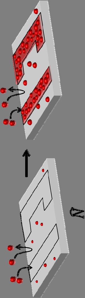
8 Inhibited Growth Nuclei form via deposition on Defects present on starting surface? Defects generated during deposition? Both? What are the defects? 8


9 Controlling Nucleation ALD Island Growth Models 2003 Alum & Green 2004 Puurunen & Vandervorst 2007 O. Nilsen et al. ALD Blocking Layers ZnO: Yan, Marks, Chang et al CVD Selectivity W, Si: Many authors Co: Yang et al Improve Understanding of Nucleation and Selectivity Metals Metals Dielectrics Dielectrics 9
.")
 2 + CH 4 B: Si O Al(CH 3 ) 2 + H 2 O Si O Al(OH) 2 + 2 CH 4 CH 4 purg ALD Nucleation:")
10 Island Growth Expected from Chemistry Steady State ALD: Brønsted Lowry acid/base reaction OH (acid) H + + CH 3 ligand (base). O : conjugate base; CH 4 is conjugate acid Surface maintains oxidation state A: Si OH + Al(CH 3 ) 3 Si O Al(CH 3 ) 2 + CH 4 B: Si O Al(CH 3 ) 2 + H 2 O Si O Al(OH) CH 4 CH 4 purg ALD Nucleation: on metal (Si) Surface changes oxidation state Si H + H 2 O Si OH (Si 0 Si +1 ) 10
11 Outline 1. Nucleation during ALD Inhibited, Island Growth 2. New model for Island Growth Use Growth Rate, Fit to starting defect density Definition of Selectivity Approach for Selective Deposition Comparison 3. Area Selective Deposition Motivation Methods to achieve selectivity Examples comparing selectivity data 4. Atomic Layer Etching 11
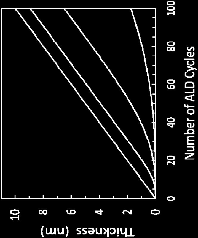
12 We can Fit Curve Using Island Growth Model Geometric Island Distribution: Puurunen and Vandervorst JAP (2004) Multi regional equation for surface coverage: 12

13 We can Fit Curve Using Island Growth Model Geometric Island Distribution: O. Nilsen et al. JAP (2007) Multi regional equation for thickness: 13


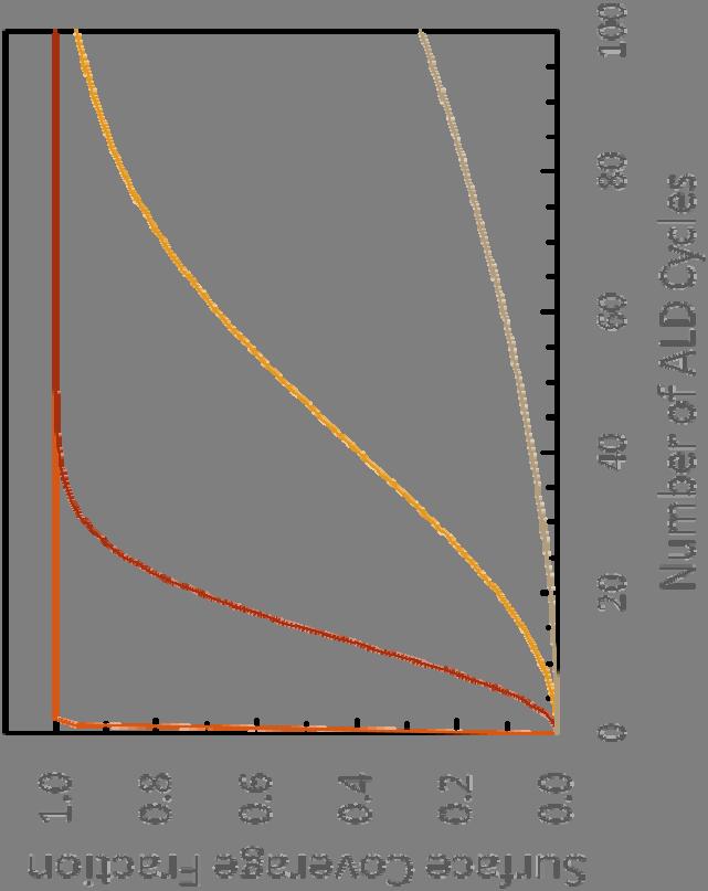
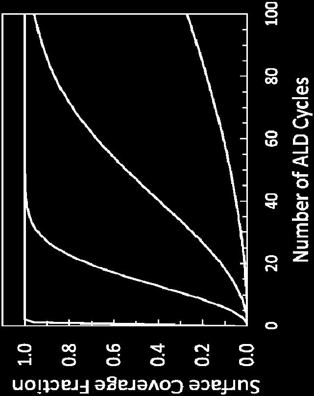
14 Random Model More Realistic than Geometric Geometric Distribution: Random Distribution: 14


15 Growth Defect Sites: Present and Created On starting surface or passivation layer Created during ALD Defects on starting surface: 0.0 Generated during ALD: 0 15


16 Shape of Curve Determined by Defect Density Fewer Defect Nucleation Sites (present or created) 16


17 Avrami Equation: Surface coverage vs time A extended = same size, no overlap > A film > A 0 (large t) easy to find vs t Growth Rate: ; and Starting Nuclei Density: During 0 : Avrami Equation: 1 17
18 Avrami Equation: Thickness vs time Surface Coverage 1 exp Film thickness vs time one equation: Need only: and to find Measure, fit 18


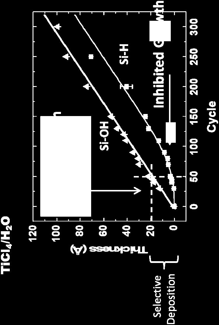
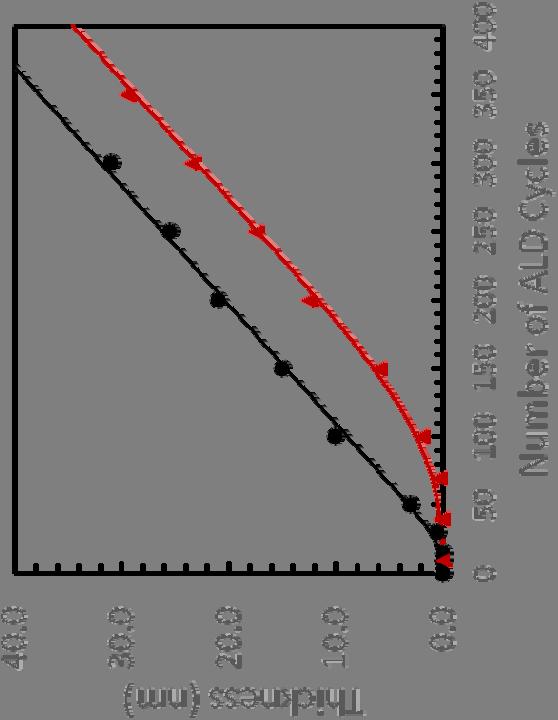
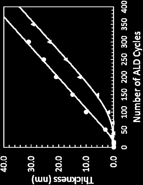
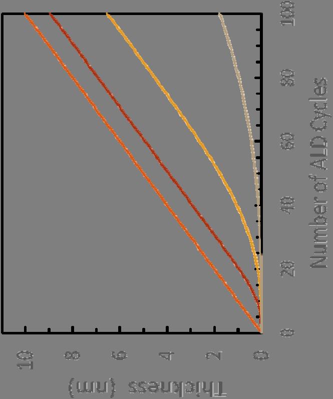
19 Measure, fit Data: HfO 2 ALD on SiO 2 and a C:H Stevens et al. Chem Mat (2018) 19


20 Avrami Model Fits Most Data Sets Green et al. JAP 2002 HfO 2 ALD: HfCl 4 /H 2 O on SiO 2 and Si H Ġ = nm/cycle N = 0.07 nm 2 R. Puurunen JAP 2004 HfO 2 ALD: HfCl 4 /H 2 O on SiO 2 and Si H Ġ = nm/cycle N = nm 2 20

21 Exception: Dynamic Coalescence Observed for Pt ALD Grillo et al. Chem Mat (2017) 21

 changes")
22 Selectivity in Chemical Reactions A Chemical Reaction: Definitions of Chemical Selectivity: Deposition Reaction: Desired Undesired Selectivity S = Thickness on 1 θ θ θ θ Selectivity S = 1 Thickness on 1 θ = Surface coverage Gladfelter, ChemMat (1993) changes with thickness 22


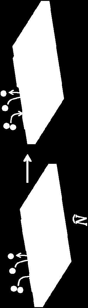
23 Definitions of Selectivity in Deposition 1. Thermodynamics: Selectivity, R G = ratio of driving force of the reaction on the desired surface to that on the undesired surface What is reaction with defects? 2. Elemental Counts: From the ratio of elemental counts, selectivity is 2000 to 1 : Depends on thickness 3. Film Thickness: Selectivity is 6 nm before substantial nucleation on nongrowth surface : Substantial? Selectivity is the amount of film we can grow in the desired region before nucleation in the non growth region sets on. Depends on measurement method 4. Film Growth Rate: These deposition rates indicate a selectivity of >185 : Depends on thickness Reinke et al. ACS AMI (2015) 23 Singh et al. Chem Mat (2018) Kalanyan et al. Chem Mat (2016) McDonnell et al. JPCC (2013) Carlsson & Boman JVSTA (1985)
24 Empirical Definition of Selectivity Gladfelter, Chem. Mat. 1993: Selectivity: θ θ θ θ S ranges from 0 to 1 θ S1, θ S2 : Coverage on growth and non growth surfaces θ s from SEM, TEM, AFM, STM, etc. Atomic %: from XPS, AES, RBS, etc. Problem: Selectivity value changes with thickness, growth time 24
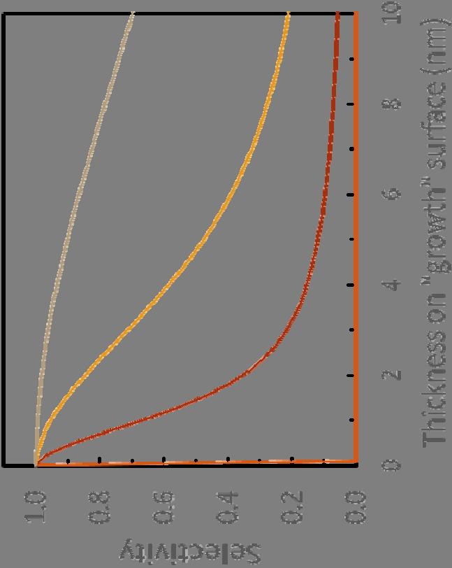
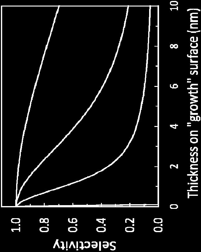
25 Nucleation Model and Definition of Selectivity Fewer nucleation sites Improved Selectivity θ θ θ θ 0.9;


26 Example: S = 0.9; t S=0.9 = 1.3 nm θ θ θ θ. Data from: Stevens et al. Chem Mat (2018) 26
27 Outline 1. Nucleation during ALD Inhibited, Island Growth 2. New model for Island Growth Use Growth Rate, Fit to starting defect density Definition of Selectivity Approach for Selective Deposition Comparison 3. Area Selective Deposition Motivation Methods to achieve selectivity Examples comparing selectivity data 4. Atomic Layer Etching 27
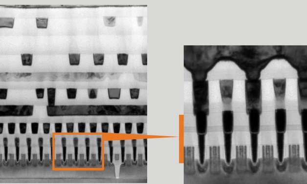
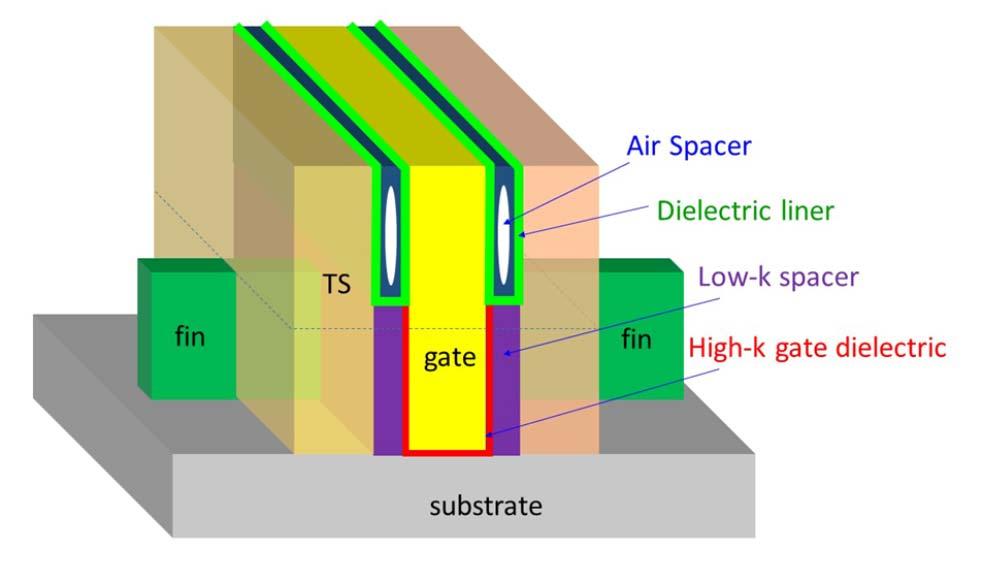
28 FIN FET Transistor


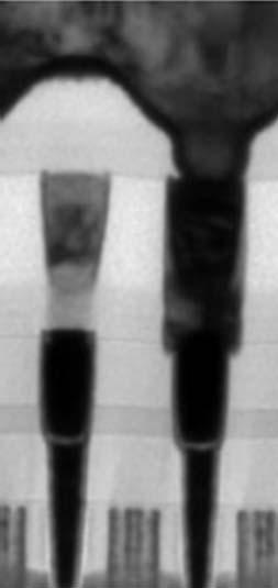
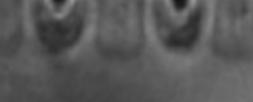
29 Self Aligned Via Used Now

30 Fully Aligned Via Needs Area Selective Deposition


31 Approaches to Area Selective Deposition Inherent Activated Passivated 31

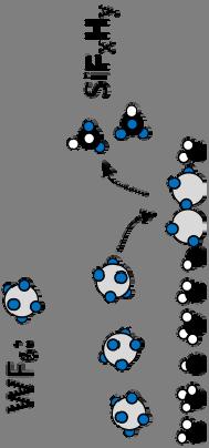
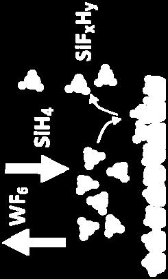
 W + SiF 4")


32 Inherent 1. Pattern Si/SiO 2 2. ALD W: WF 6 + Si (s) W + SiF 4 : G<<0 WF 6 + SiO 2 : G>> Kalanyan et al. Chem Mat (2016) 32


 0.04 0.")
33 Activated 1. Electron/ion beam + MeCpPtMe 3 P O2 = 2 mtorr 2. ALD Pt: MeCpPtMe 3 /O 2 at 300 C Mackus et al. JPPC (2013) P O2 = 800 mtorr 33

34 Activated 1. Pattern Pt 2. ALD Fe 2 O 3 : O 2 / t butyl ferrocene at 250 C 20 nm Singh et al. Chem Mat (2018) 34
35 Passivated Hydrophobic Hydrophilic Precursor Pulse No adsorption on SAM Argon Purge Reactant Pulse Argon Purge KJ Park et al. APL (2005) 35
 monolayer on")
hafnium Hf(N(CH 3 ) 2 ) 4 + H 2")
36 Passivated 1. Solution coating of octadecyl trichlorosilane (ODTS) monolayer on patterned SiO 2 2. HfO 2 ALD:Tetrakis(dimethyl amido)hafnium Hf(N(CH 3 ) 2 ) 4 + H 2 O Deposition only on Si H regions Auger No growth on oxide/odts regions R.Chen et al. APL (2005) 36


37 Renew surface and extend selectivity Etching, Removal, Cleaning add third step. Single step Multiple steps Deposition: Etch/Renew: Repeat 37
38 Passivation + Removal 1. Solution deposit octadecylphosphonic acid (ODPA) SAM on Copper 2. Al 2 O 3 ALD: TMA/H 2 O at 150C 3. Acetic acid wet etch removes SAM and nuclei After wet etch: Fit Quality? Hashemi et al. ACS Nano (2015) 38

39 Passivation + Regeneration SAM Vapor 1. Vapor deposit dodecanethiol (DDT) SAM on Copper 2. ZnO ALD: DEZ/H 2 O at 150C 3. Repeat Fit Quality? Hashemi et al. ACS AMI (2016) 39

40 In situ Cleaning 1. Pattern Cu/SiO 2 2. ZrO 2 ALD: ZyALD/Ethanol at 200C 3. Ethanol reduces CuO, inhibits ALD 2 3nm Selvaraj et al. JVST (2014) 40
 2 ] 2 ) & O 2 plasma 3. Repeat Mameli et al.")
41 In situ Gas Phase Inhibition 1. Expose Hacac (vapor inhibitor) to patterned SiO 2 /Al 2 O 3, adsorbs on SiO 2 2. One cycle of SiO 2 Plasma ALD: BDEAS (H 2 Si[N(C 2 H 5 ) 2 ] 2 ) & O 2 plasma 3. Repeat Mameli et al. ACS Nano (2017) 41


42 ALD + Etching 1. ~4 cycles Ta 2 O 5 Plasma ALD: TBTDET & O 2 on pattern TiN/SiO 2 surface 2. NF 3 plasma etch 3. Repeat Deposition Deposition + Etch Vallat et al. JVSTA (2017) 42


43 Tungsten ALD: W on Al 2 O 3 ALD Cycle Number 43
 + TiF 4(g) W, Ti volatile Al + W + O + F at Equilibrium: < 100C: WO 3(s) + AlF 3(s) 220C: WO 2 F")
 WO 3(s) WF 6(g) TiF 4(g) HSC Chemistry 7.")
44 WF 6 etches TiO 2 but not Al 2 O 3 Not Self limiting Ti + W + O + F at Equilibrium: < 100C: WO 3(s) + TiF 4(s) 220C: WO 2 F 2(g) + TiF 4(g) W, Ti volatile Al + W + O + F at Equilibrium: < 100C: WO 3(s) + AlF 3(s) 220C: WO 2 F 2(g) + AlF 3(s) Solid Equilibrium Concentration (mol) TiF 4(s) WO 3(s) WF 6(g) TiF 4(g) HSC Chemistry 7.1 WF 2 O 2(g) Equilibrium Thermo Calculation No Etching Etching 220C Temperature ( C) 44
45 Outline 1. Nucleation during ALD Inhibited, Island Growth 2. New model for Island Growth Use Growth Rate, Fit to starting defect density Definition of Selectivity Approach for Selective Deposition Comparison 3. Area Selective Deposition Motivation Methods to achieve selectivity Examples comparing selectivity data 4. Atomic Layer Etching 45

46 Self Limiting Plasma/Ion Atomic Layer Etching C.T. Carver et al. ECS J. Sol. St. Sci. and Tech. (2015) 46
47 Self Limiting Thermal Atomic Layer Etching Younghee Lee and S.M. George, ACS Nano (2015) 47


48 Self Limiting Thermal Atomic Layer Etching Younghee Lee, C. Huffman, S.M. George, Chem Mat (2016) 48

49 Self Limiting Thermal Atomic Layer Etching Younghee Lee, C. Huffman, S.M. George, Chem Mat (2016) 49
")
 BF 3(g) + WOCl 4(g) + TiCl")


50 Self Limiting ALE: TiO 2 + WF 6 /BCl 3 190C: WF 6 + TiO 2 WO 3(s) + TiF 4(s) BCl 3 + WO 3(s) + TiF 4(s) BF 3(g) + WOCl 4(g) + TiCl 4(g) + B 2 O 3(s) Quartz Crystal Microbalance 170C W species volatile HSC Chemistry 7.1 Atomic Layer Etching Lemaire & Parsons, Chem Mat (2017)

51 Selective Area CVD of Cobalt CVD chemistry currently ahead of ALD for selective deposition Selective Co CVD Up to 9 nm C. C.Yang et al. Microelectronic Engineering (2013) 51
52 Summary 1. Nucleation during ALD Inhibited, Island Growth 2. New model for Island Growth Use Growth Rate, Fit to starting defect density Definition of Selectivity Approach for Selective Deposition Comparison 3. Area Selective Deposition Motivation Methods to achieve selectivity Examples comparing selectivity data 4. Atomic Layer Etching 52
Reaction Mechanism of Area-Selective Atomic
 Supporting Information Reaction Mechanism of Area-Selective Atomic Layer Deposition for Al 2 O 3 Nanopatterns Seunggi Seo 1, Il-Kwon Oh 1, Byung Chul Yeo 1, 2, Sang Soo Han 2, Chang Mo Yoon 1, JOON YOUNG
ALD-enabled nanopatterning: area-selective ALD by area-activation
 ALD-enabled nanopatterning: area-selective ALD by area-activation Adrie Mackus, Ageeth Bol, and Erwin Kessels w.m.m.kessels@tue.nl www.tue.nl/pmp Outline Introduction & Area-selective deposition Area-selective
In situ Studies of ALD Processes & Reaction Mechanisms
 In situ Studies of ALD Processes & Reaction Mechanisms Erwin Kessels w.m.m.kessels@tue.nl www.tue.nl/pmp This tutorial presentation will give (1) an overview of methods for in situ studies of ALD processes
Selective Processes: Challenges and Opportunities in Semiconductor Scaling
 Selective Processes: Challenges and Opportunities in Semiconductor Scaling June 4, 2018 Kandabara Tapily TEL Technology Center, America, LLC IITC 2018 Selective Deposition Workshop K. Tapily/ IITC 2018
Step Coverage by ALD Films: Theory and Examples
 Step Coverage by ALD Films: Theory and Examples of Ideal and Non-Ideal Reactions Roy G. Gordon Cambridge, MA 1 L Step Coverage in Holes with High Aspect Ratio Step coverage = (b/a) x 100% a Aspect ratio
Hotwire-assisted Atomic Layer Deposition of Pure Metals and Metal Nitrides
 Hotwire-assisted Atomic Layer Deposition of Pure Metals and Metal Nitrides Alexey Kovalgin MESA+ Institute for Nanotechnology Semiconductor Components group a.y.kovalgin@utwente.nl 1 Motivation 1. Materials
Procédés de dépôt plasma avec injection pulsée de précurseurs (PECVD et PEALD) :
 :") Procédés de dépôt plasma avec injection pulsée de précurseurs (PECVD et PEALD) : Impact du réacteur et de la pression et développement de dépôts sélectifs C. Vallée 1,3, R. Gassilloud 2, R. Vallat 1,2,
Procédés de dépôt plasma avec injection pulsée de précurseurs (PECVD et PEALD) : Impact du réacteur et de la pression et développement de dépôts sélectifs C. Vallée 1,3, R. Gassilloud 2, R. Vallat 1,2,
Initial Stages of Growth of Organic Semiconductors on Graphene
 Initial Stages of Growth of Organic Semiconductors on Graphene Presented by: Manisha Chhikara Supervisor: Prof. Dr. Gvido Bratina University of Nova Gorica Outline Introduction to Graphene Fabrication
ABSTRACT. prohibitively expensive, requires innovations in process design and chemistry. Atomic layer
 ABSTRACT STEVENS, ERIC CHRISTOPHER. From Novel Processes to Industrially Relevant Applications: Atomic Layer Deposition of Metal, Metal Oxide, and Metal Carbide Thin Films. (Under the direction of Dr.
ABSTRACT. LEMAIRE, PAUL CHARLES. Atomic Layer Deposition and Controlling Film and Crystal Nucleation. (Under the direction of Gregory N. Parsons).
.") ABSTRACT LEMAIRE, PAUL CHARLES. Atomic Layer Deposition and Controlling Film and Crystal Nucleation. (Under the direction of Gregory N. Parsons). Typically, conformally coating fibers or high aspect ratio
ABSTRACT LEMAIRE, PAUL CHARLES. Atomic Layer Deposition and Controlling Film and Crystal Nucleation. (Under the direction of Gregory N. Parsons). Typically, conformally coating fibers or high aspect ratio
Simulating mechanism at the atomic-scale for atomically precise deposition and etching
 SEMICON TechArena session on Advanced Materials 14 November 2017 Simulating mechanism at the atomic-scale for atomically precise deposition and etching Simon D. Elliott & Ekaterina Filatova simon.elliott@tyndall.ie
Lecture 10 Thin Film Growth
 Lecture 10 Thin Film Growth 1/76 Announcements Homework: Homework Number 2 is returned today, please pick it up from me at the end of the class. Solutions are online. Homework 3 will be set Thursday (2
Atomic Layer Processing:
 Nano and Giga Challenges in Electronics, Photonics and Renewable Energy Tomsk, Russia, Sept. 18-22, 2017 Atomic Layer Processing: basics, materials, processes & applications Fred Roozeboom TU Eindhoven
Atomic Layer Deposition: An Overview
 Chem. Rev. 2010, 110, 111 131 111 Atomic Layer Deposition: An Overview Steven M. George* Department of Chemistry and Biochemistry and Department of Chemical and Biological Engineering, University of Colorado,
Short course on Atomic Layer Deposition
 Short course on Atomic Layer Deposition Erwin Kessels & Jan-Pieter van Delft w.m.m.kessels@tue.nl www.phys.tue.nl/pmp Vapor phase deposition technologies Physical Vapor Deposition (PVD) sputtering Chemical
TiO2/sapphire Beam Splitter for High-order Harmonics
 Technical Communication TiO2/sapphire Beam Splitter for High-order Harmonics Y. Sanjo*1, M. Murata*1, Y. Tanaka*1, H. Kumagai*1, and M. Chigane*2 *1 Graduate School of Engineering,Osaka City University,
Hydrogenation of Single Walled Carbon Nanotubes
 Hydrogenation of Single Walled Carbon Nanotubes Anders Nilsson Stanford Synchrotron Radiation Laboratory (SSRL) and Stockholm University Coworkers and Ackowledgement A. Nikitin 1), H. Ogasawara 1), D.
Ligand coated metal nanoparticles and quantum dots
 The Supramolecular Nano Materials Group Ligand coated metal nanoparticles and quantum dots Francesco Stellacci Department of Materials Science and Engineering frstella@mit.edu Outline Self-Assembled Monolayers
Molecular Dynamics on the Angstrom Scale
 Probing Interface Reactions by STM: Molecular Dynamics on the Angstrom Scale Zhisheng Li Prof. Richard Osgood Laboratory for Light-Surface Interactions, Columbia University Outline Motivation: Why do we
EE C245 ME C218 Introduction to MEMS Design Fall 2007
 EE C245 ME C218 Introduction to MEMS Design Fall 2007 Prof. Clark T.-C. Nguyen Dept. of Electrical Engineering & Computer Sciences University of California at Berkeley Berkeley, CA 94720 Lecture 4: Film
Kinetic Monte Carlo Simulation of Two-dimensional Semiconductor Quantum Dots Growth
 Kinetic Monte Carlo Simulation of Two-dimensional Semiconductor Quantum Dots Growth by Ernie Pan Richard Zhu Melissa Sun Peter Chung Computer Modeling and Simulation Group The University of Akron Outline
Déposition séléctive le rêve reviens
 Willkommen Welcome Bienvenue Déposition séléctive le rêve reviens Patrik Hoffmann Michael Reinke, Yury Kuzminykh Ivo Utke, Carlos Guerra-Nunez, Ali Dabirian, Xavier Multone, Tristan Bret, Estelle Halary-Wagner,
Fabrication at the nanoscale for nanophotonics
 Fabrication at the nanoscale for nanophotonics Ilya Sychugov, KTH Materials Physics, Kista silicon nanocrystal by electron beam induced deposition lithography Outline of basic nanofabrication methods Devices
Section 3: Etching. Jaeger Chapter 2 Reader
 Section 3: Etching Jaeger Chapter 2 Reader Etch rate Etch Process - Figures of Merit Etch rate uniformity Selectivity Anisotropy d m Bias and anisotropy etching mask h f substrate d f d m substrate d f
Agenda. 1. Atomic Layer Deposition Technology
 Agenda 1. Atomic Layer Deposition Technology 2. What is ALD? Atomic Layer Deposition is invented in 1977 by T. Suntola et al. - New Deposition Method for Electro-Luminescent Display (ZnS:Mn Thin Films)
Layer-modulated synthesis of uniform tungsten disulfide nanosheet using gas-phase precursors.
 Layer-modulated synthesis of uniform tungsten disulfide nanosheet using gas-phase precursors. Jusang Park * Hyungjun Kim School of Electrical and Electronics Engineering, Yonsei University, 262 Seongsanno,
Special Properties of Au Nanoparticles
 Special Properties of Au Nanoparticles Maryam Ebrahimi Chem 7500/750 March 28 th, 2007 1 Outline Introduction The importance of unexpected electronic, geometric, and chemical properties of nanoparticles
ALD & ALE Tutorial Speakers and Schedule
 ALD & ALE Tutorial Speakers and Schedule Sunday, July 29, 2018 1:00-1:05 Tutorial Welcome 1:05-1:50 1:50-2:35 2:35-3:20 Challenges of ALD Applications in Memory Semiconductor Devices, Choon Hwan Kim (SK
Complex Nanostructures by Atomic Layer Deposition. Kornelius Nielsch.
 Complex Nanostructures by Atomic Layer Deposition Kornelius Nielsch Institute of Applied Physics, University of Hamburg (Germany) knielsch@physnet.uni-hamburg.de Outline History and Principle Ferromagnetic
Real-Time Chemical Sensing for Advanced Process Control in ALD
 Real-Time Chemical Sensing for Advanced Process Control in ALD Gary W. Rubloff 1, Laurent Henn-Lecordier 2, and Wei Lei 3 University of Maryland 1 Director, Maryland Center for Integrated Nano Science
Competition between Al 2 O 3 Atomic Layer Etching and AlF 3 Atomic Layer Deposition Using Sequential Exposures of Trimethylaluminum and HF
 Revised J. Chem. Phys. Manuscript No. AMLP16.08.0222 December 5, 2016 Competition between Al 2 O 3 Atomic Layer Etching and AlF 3 Atomic Layer Deposition Using Sequential Exposures of Trimethylaluminum
Atomic Layer Deposition in Food Packaging and Barrier Coatings
 Atomic Layer Deposition in Food Packaging and Barrier Coatings Cost Workshop 16 th September2011, Espoo Dr. Pirjo Heikkilä VTT Technical Research Centre of Finland 2 Outline of the Presentation Food packaging
Vapor phase deposition and characterization of nanoporous films
 Vapor phase deposition and characterization of nanoporous films Cluster innovatieve coatings, March 23, 2018 Corda Campus Hasselt Rob Ameloot Center for Surface Chemistry and Catalysis KU Leuven University
EE143 Fall 2016 Microfabrication Technologies. Lecture 6: Thin Film Deposition Reading: Jaeger Chapter 6
 EE143 Fall 2016 Microfabrication Technologies Lecture 6: Thin Film Deposition Reading: Jaeger Chapter 6 Prof. Ming C. Wu wu@eecs.berkeley.edu 511 Sutardja Dai Hall (SDH) 1 Vacuum Basics Units 1 atmosphere
Supporting Information
 Supporting Information Yao et al. 10.1073/pnas.1416368111 Fig. S1. In situ LEEM imaging of graphene growth via chemical vapor deposition (CVD) on Pt(111). The growth of graphene on Pt(111) via a CVD process
Lecture 30: Kinetics of Epitaxial Growth: Surface Diffusion and
 Lecture 30: Kinetics of Epitaxial Growth: Surface Diffusion and Nucleation Today s topics Understanding the basics of epitaxial techniques used for surface growth of crystalline structures (films, or layers).
EE C245 ME C218 Introduction to MEMS Design Fall 2007
 EE C245 ME C218 Introduction to MEMS Design Fall 2007 Prof. Clark T.-C. Nguyen Dept. of Electrical Engineering & Computer Sciences University of California at Berkeley Berkeley, CA 94720 Lecture 5: ALD,
Reactive Ion Etching (RIE)
") Reactive Ion Etching (RIE) RF 13.56 ~ MHz plasma Parallel-Plate Reactor wafers Sputtering Plasma generates (1) Ions (2) Activated neutrals Enhance chemical reaction 1 2 Remote Plasma Reactors Plasma Sources
Reactive Ion Etching (RIE) RF 13.56 ~ MHz plasma Parallel-Plate Reactor wafers Sputtering Plasma generates (1) Ions (2) Activated neutrals Enhance chemical reaction 1 2 Remote Plasma Reactors Plasma Sources
CVD: General considerations.
 CVD: General considerations. PVD: Move material from bulk to thin film form. Limited primarily to metals or simple materials. Limited by thermal stability/vapor pressure considerations. Typically requires
On adsorption of aluminium and methyl groups on silica for TMA/H 2 O process in atomic layer deposition of aluminium oxide nano layers
 Bull. Mater. Sci., Vol. 33, No. 2, April 2010, pp. 97 102. Indian Academy of Sciences. On adsorption of aluminium and methyl groups on silica for TMA/H 2 O process in atomic layer deposition of aluminium
Selective-Area Atomic Layer Deposition of Copper Nanostructures for Direct Electro- Optical Solar Energy Conversion
 Selective-Area Atomic Layer Deposition of Copper Nanostructures for Direct Electro- Optical Solar Energy Conversion Brian Willis UCONN Cancun, MX 2014 Plasmonics Au, Ag, Cu Nanoparticles interact strongly
SEMICONDUCTOR GROWTH TECHNIQUES. Introduction to growth techniques (bulk, epitaxy) Basic concepts in epitaxy (MBE, MOCVD)
 Basic concepts in epitaxy (MBE, MOCVD)") SEMICONDUCTOR GROWTH TECHNIQUES Introduction to growth techniques (bulk, epitaxy) Basic concepts in epitaxy (MBE, MOCVD) Growth Processes Bulk techniques (massive semiconductors, wafers): Si, compounds
SEMICONDUCTOR GROWTH TECHNIQUES Introduction to growth techniques (bulk, epitaxy) Basic concepts in epitaxy (MBE, MOCVD) Growth Processes Bulk techniques (massive semiconductors, wafers): Si, compounds
DEPOSITION AND COMPOSITION OF POLYMER FILMS IN FLUOROCARBON PLASMAS*
 DEPOSITION AND COMPOSITION OF POLYMER FILMS IN FLUOROCARBON PLASMAS* Kapil Rajaraman and Mark J. Kushner 1406 W. Green St. Urbana, IL 61801 rajaramn@uiuc.edu mjk@uiuc.edu http://uigelz.ece.uiuc.edu November
Luigi Colombo. Texas Instruments Incorporated Dallas, TX, USA. Graphene Conference: From Research to Applications Oct 2012
 Luigi Colombo Texas Instruments Incorporated Dallas, TX, USA Graphene Conference: From Research to Applications 15-16 Oct 2012 NPL,UK UT Austin - Banerjee group UT Austin - Tutuc group UT Austin Ruoff
On the nucleation of Pt & Pd during atomic layer deposition & temperature programmed desorption for thin film analysis
 Eindhoven University of Technology MASTER On the nucleation of Pt & Pd during atomic layer deposition & temperature programmed desorption for thin film analysis Vervuurt, R.H.J. Award date: 2012 Link to
Wafer Scale Homogeneous Bilayer Graphene Films by. Chemical Vapor Deposition
 Supporting Information for Wafer Scale Homogeneous Bilayer Graphene Films by Chemical Vapor Deposition Seunghyun Lee, Kyunghoon Lee, Zhaohui Zhong Department of Electrical Engineering and Computer Science,
Prediction and accelerated laboratory discovery of heterogeneous catalysts
 Prediction and accelerated laboratory discovery of heterogeneous catalysts Kenneth R. Poeppelmeier Charles E. and Emma H. Morrison Professor of Chemistry Department of Chemistry 2145 Sheridan Road Evanston,
Effective Capacitance Enhancement Methods for 90-nm DRAM Capacitors
 Journal of the Korean Physical Society, Vol. 44, No. 1, January 2004, pp. 112 116 Effective Capacitance Enhancement Methods for 90-nm DRAM Capacitors Y. K. Park, Y. S. Ahn, S. B. Kim, K. H. Lee, C. H.
Supplementary Figure 1 Experimental setup for crystal growth. Schematic drawing of the experimental setup for C 8 -BTBT crystal growth.
 Supplementary Figure 1 Experimental setup for crystal growth. Schematic drawing of the experimental setup for C 8 -BTBT crystal growth. Supplementary Figure 2 AFM study of the C 8 -BTBT crystal growth
There's Plenty of Room at the Bottom
 There's Plenty of Room at the Bottom 12/29/1959 Feynman asked why not put the entire Encyclopedia Britannica (24 volumes) on a pin head (requires atomic scale recording). He proposed to use electron microscope
Hydrophilization of Fluoropolymers and Silicones
 2017 Adhesive and Sealant Council Spring Meeting Hydrophilization of Fluoropolymers and Silicones Aknowledgements: Wei Chen Mount Holyoke College NSF, NIH, Dreyfus, ACS-RF, MHC Bryony Coupe, Mamle Quarmyne,
Chemical Vapor Deposition (CVD)
") Chemical Vapor Deposition (CVD) source chemical reaction film substrate More conformal deposition vs. PVD t Shown here is 100% conformal deposition ( higher temp has higher surface diffusion) t step 1
Chemical Vapor Deposition (CVD) source chemical reaction film substrate More conformal deposition vs. PVD t Shown here is 100% conformal deposition ( higher temp has higher surface diffusion) t step 1
Multiscale Simulation of Atomic Layer Deposition in a Nanoporous Material
 The Institute for Systems Research Isr Technical Report 28-21 Multiscale Simulation of Atomic Layer Deposition in a Nanoporous Material Dwivedi, Vivek, and Adomaitis, Raymond ISR develops, applies and
Quantum confined materials
 Quantum confined materials Quantum Wells Quantum wells structures can be fabricated by seeral methods in semiconductors alloys. A quantum well is fabricated by depositing ery thin layers of different materials
3.46 PHOTONIC MATERIALS AND DEVICES Lecture 15: III-V Processing
 3.46 PHOTONIC MATERIALS AND DEVICES 15: III-V Processing Double Hetero structure laser (band structure engineering) AlGaAs GaAs AlGaAs e - E n hν P h + X n x I d < 1 μm 1. Large refractive index active
2.1 Template Method Microemulsion Nanostructured Polymer (Copolymer, DNA) Nanostructured Ceramics (AAO, Porous Silica, Zeolite)
 Nanostructured Ceramics (AAO, Porous Silica, Zeolite)") Chapter 1. Characteristics of Nanomaterials Chapter 2. Methodology of Nanomaterials 2.1 Template Method 2.1.1. Microemulsion 2.1.2. Nanostructured Polymer (Copolymer, DNA) 2.1.3. Nanostructured Ceramics
Chapter 1. Characteristics of Nanomaterials Chapter 2. Methodology of Nanomaterials 2.1 Template Method 2.1.1. Microemulsion 2.1.2. Nanostructured Polymer (Copolymer, DNA) 2.1.3. Nanostructured Ceramics
Surface Functionalization by Atomic Layer Deposition
 Surface Functionalization by Atomic Layer Deposition Christophe Detavernier SIM User Forum - Gent 27/10/2015 CoCooN Conformal Coating of Nanomaterials Atomic layer deposition (ALD) Gas-phase thin film
Fundamental insight into ALD processing by in-
 Fakultät Elektrotechnik und Informationstechnik Institut für Halbleiter- und Mikrosystemtechnik Fundamental insight into ALD processing by in- situ observation Johann W. Bartha M. Albert, M. Junige and
JOHN G. EKERDT RESEARCH FOCUS
 JOHN G. EKERDT RESEARCH FOCUS We study the surface, growth and materials chemistry of ultrathin metal and dielectric films. Our work seeks to: 1) develop and understand the reactions and chemistry that
SYNTHESIS OF INORGANIC MATERIALS AND NANOMATERIALS. Pr. Charles Kappenstein LACCO, Laboratoire de Catalyse en Chimie Organique, Poitiers, France
 SYNTHESIS OF INORGANIC MATERIALS AND NANOMATERIALS Pr. Charles Kappenstein LACCO, Laboratoire de Catalyse en Chimie Organique, Poitiers, France Outline IV - FORMATION OF SOLIDS FROM SOLUTIONS 1) Glass
Carbon Nanotubes for Interconnect Applications Franz Kreupl, Andrew P. Graham, Maik Liebau, Georg S. Duesberg, Robert Seidel, Eugen Unger
 Carbon Nanotubes for Interconnect Applications Franz Kreupl, Andrew P. Graham, Maik Liebau, Georg S. Duesberg, Robert Seidel, Eugen Unger Infineon Technologies Corporate Research Munich, Germany Outline
ABSTRACT. using atomic layer deposition (ALD) for the deposition of thin metal oxide films. Atomic
 for the deposition of thin metal oxide films. Atomic") ABSTRACT MCCLURE, CHRISTINA DEVINE. Atomic Layer Deposition for the Modification of Polymers and Carbon Nanotubes. (Under the direction of Gregory N. Parsons). Nanoscale materials such as polymer nanofibers
ABSTRACT MCCLURE, CHRISTINA DEVINE. Atomic Layer Deposition for the Modification of Polymers and Carbon Nanotubes. (Under the direction of Gregory N. Parsons). Nanoscale materials such as polymer nanofibers
High-density data storage: principle
 High-density data storage: principle Current approach High density 1 bit = many domains Information storage driven by domain wall shifts 1 bit = 1 magnetic nanoobject Single-domain needed Single easy axis
Document Version Publisher s PDF, also known as Version of Record (includes final page, issue and volume numbers)
") Plasma-assisted ALD for the conformal deposition of SiO2 : process, material and electronic properties Dingemans, G.; Helvoirt, van, C.A.A.; Pierreux, D.; Keuning, W.; Kessels, W.M.M. Published in: Journal
Plasma-assisted ALD for the conformal deposition of SiO2 : process, material and electronic properties Dingemans, G.; Helvoirt, van, C.A.A.; Pierreux, D.; Keuning, W.; Kessels, W.M.M. Published in: Journal
Supplementary Material for
 www.sciencemag.org/cgi/content/full/science.aac6368/dc1 Supplementary Material for Identification of active sites in CO oxidation and water-gas shift over supported Pt catalysts Kunlun Ding, Ahmet Gulec,
Supplementary Information
 Supplementary Information Supplementary Figure 1. fabrication. A schematic of the experimental setup used for graphene Supplementary Figure 2. Emission spectrum of the plasma: Negative peaks indicate an
Fabrication Technology, Part I
 EEL5225: Principles of MEMS Transducers (Fall 2004) Fabrication Technology, Part I Agenda: Microfabrication Overview Basic semiconductor devices Materials Key processes Oxidation Thin-film Deposition Reading:
MS482 Materials Characterization ( 재료분석 ) Lecture Note 12: Summary. Byungha Shin Dept. of MSE, KAIST
 Lecture Note 12: Summary. Byungha Shin Dept. of MSE, KAIST") 2015 Fall Semester MS482 Materials Characterization ( 재료분석 ) Lecture Note 12: Summary Byungha Shin Dept. of MSE, KAIST 1 Course Information Syllabus 1. Overview of various characterization techniques (1
2015 Fall Semester MS482 Materials Characterization ( 재료분석 ) Lecture Note 12: Summary Byungha Shin Dept. of MSE, KAIST 1 Course Information Syllabus 1. Overview of various characterization techniques (1
CHIMICA DELLE SUPERFICI ED INTERFASI
 CHIMICA DELLE SUPERFICI ED INTERFASI DOTT. GIULIA FIORAVANTI UNIVERSITÀ DEGLI STUDI DELL AQUILA LAUREA MAGISTRALE IN INGEGNERIA CHIMICA A.A. 2013-2014 OUTLINE SURFACE CHEMICAL GRADIENTS DROPLET MOVEMENT
X-ray absorption spectroscopy of indium nitride, indium oxide, and their alloys Jiraroj T-Thienprasert, Suranaree University of Technology
 TF_O3 TF_O4 TF_O5 TF_O6 TF_O7 TF_O8 TF_O9 TF_O10 TF_O11 X-ray absorption spectroscopy of indium nitride, indium oxide, and their alloys Jiraroj T-Thienprasert, Suranaree University of Technology Structural
A new method of growing graphene on Cu by hydrogen etching
 A new method of growing graphene on Cu by hydrogen etching Linjie zhan version 6, 2015.05.12--2015.05.24 CVD graphene Hydrogen etching Anisotropic Copper-catalyzed Highly anisotropic hydrogen etching method
Scaling up Chemical Vapor Deposition Graphene to 300 mm Si substrates
 Scaling up Chemical Vapor Deposition Graphene to 300 mm Si substrates Co- Authors Aixtron Alex Jouvray Simon Buttress Gavin Dodge Ken Teo The work shown here has received partial funding from the European
Removal of Cu Impurities on a Si Substrate by Using (H 2 O 2 +HF) and (UV/O 3 +HF)
 and (UV/O 3 +HF)") Journal of the Korean Physical Society, Vol. 33, No. 5, November 1998, pp. 579 583 Removal of Cu Impurities on a Si Substrate by Using (H 2 O 2 +HF) and (UV/O 3 +HF) Baikil Choi and Hyeongtag Jeon School
Journal of the Korean Physical Society, Vol. 33, No. 5, November 1998, pp. 579 583 Removal of Cu Impurities on a Si Substrate by Using (H 2 O 2 +HF) and (UV/O 3 +HF) Baikil Choi and Hyeongtag Jeon School
Focused Ion Beam Induced Local Tungsten Deposition
 Focused Ion Beam Induced Local Tungsten Deposition H. Langfischer, B. Basnar, E. Bertagnolli Institute for Solid State Electronics, Vienna University of Technology, Floragasse 7, 1040 ien, Austria H. Hutter
IV. Surface analysis for chemical state, chemical composition
 IV. Surface analysis for chemical state, chemical composition Probe beam Detect XPS Photon (X-ray) Photoelectron(core level electron) UPS Photon (UV) Photoelectron(valence level electron) AES electron
In-situ Monitoring of Thin-Film Formation Processes by Spectroscopic Ellipsometry
 In-situ Monitoring of Thin-Film Formation Processes by Spectroscopic Ellipsometry Alexey Kovalgin Chair of Semiconductor Components MESA+ Institute for Nanotechnology Motivation Advantages of in-situ over
Subnanometre platinum clusters as highly active and selective catalysts for the oxidative dehydrogenation of propane
 DOI: 10.1038/NMAT2384 Subnanometre platinum clusters as highly active and selective catalysts for the oxidative dehydrogenation of propane Stefan Vajda, Larry A. Curtiss, Peter Zapol et al. Center for
The goal of this project is to enhance the power density and lowtemperature efficiency of solid oxide fuel cells (SOFC) manufactured by atomic layer
 manufactured by atomic layer") Stanford University Michael Shandalov1, Shriram Ramanathan2, Changhyun Ko2 and Paul McIntyre1 1Department of Materials Science and Engineering, Stanford University 2Division of Engineering and Applied
Stanford University Michael Shandalov1, Shriram Ramanathan2, Changhyun Ko2 and Paul McIntyre1 1Department of Materials Science and Engineering, Stanford University 2Division of Engineering and Applied
Plasma-Surface Interactions in Patterning High-k k Dielectric Materials
 Plasma-Surface Interactions in Patterning High-k k Dielectric Materials October 11, 4 Feature Level Compensation and Control Seminar Jane P. Chang Department of Chemical Engineering University of California,
Surface atoms/molecules of a material act as an interface to its surrounding environment;
 1 Chapter 1 Thesis Overview Surface atoms/molecules of a material act as an interface to its surrounding environment; their properties are often complicated by external adsorbates/species on the surface
Thin-Film Deposition of Silicon Nitrides and Oxides from Trihydridosilanes. Albany, NY 12203, USA
 Thin-Film Deposition of Silicon Nitrides and Oxides from Trihydridosilanes B. Arkles a, Y. Pan a and A. E. Kaloyeros b a Gelest Inc., 11 East Steel d. Morrisville, PA 19067, USA b College of Nanoscale
Wafer-Scale Single-Domain-Like Graphene by. Defect-Selective Atomic Layer Deposition of
 Electronic Supplementary Material (ESI) for Nanoscale. This journal is The Royal Society of Chemistry 2015 Wafer-Scale Single-Domain-Like Graphene by Defect-Selective Atomic Layer Deposition of Hexagonal
Supporting Information
 Supporting Information Robust Co-Catalytic Performance of Nanodiamonds Loaded on WO 3 for the Decomposition of Volatile Organic Compounds under Visible Light Hyoung il Kim, a Hee-na Kim, a Seunghyun Weon,
Identification of droplet-flow-induced electric energy on electrolyte-insulator-semiconductor structure
 Supporting Information for Identification of droplet-flow-induced electric energy on electrolyte-insulator-semiconductor structure Junwoo Park, Suhwan Song, YoungJun Yang, Soon-Hyung Kwon,, Eunji Sim,
The Pennsylvania State University. Kurt J. Lesker Company. North Carolina State University. Taiwan Semiconductor Manufacturing Company 1
 Enhancement Mode Strained (1.3%) Germanium Quantum Well FinFET (W fin =20nm) with High Mobility (μ Hole =700 cm 2 /Vs), Low EOT (~0.7nm) on Bulk Silicon Substrate A. Agrawal 1, M. Barth 1, G. B. Rayner
Modern Methods in Heterogeneous Catalysis Research: Preparation of Model Systems by Physical Methods
 Modern Methods in Heterogeneous Catalysis Research: Preparation of Model Systems by Physical Methods Methods for catalyst preparation Methods discussed in this lecture Physical vapour deposition - PLD
Lecture 15 Etching. Chapters 15 & 16 Wolf and Tauber. ECE611 / CHE611 Electronic Materials Processing Fall John Labram 1/76
 Lecture 15 Etching Chapters 15 & 16 Wolf and Tauber 1/76 Announcements Term Paper: You are expected to produce a 4-5 page term paper on a selected topic (from a list). Term paper contributes 25% of course
Highly stable and flexible Li-ion battery anodes based on TiO 2 coated
 Electronic Supplementary Material (ESI) for Journal of Materials Chemistry A. This journal is The Royal Society of Chemistry 2015 Supporting Information for Highly stable and flexible Li-ion battery anodes
Towards Graphene-based heterojunction devices for microelectronic applications
 Towards Graphene-based heterojunction devices for microelectronic applications IHP GmbH Leibniz (Innovations for High Performance Microelectronics) TU-Dresden/IHM (Institute of Semiconductors and Microsystems)
Epitaxial Growth of Mn on Si(111)
") 105 Chapter 7 Epitaxial Growth of Mn on Si(111) 7.1 Introduction There are a few reports and experiments concerning the adsoption of Mn on Si(111), where film growth with and without a Bi surfactant layer
105 Chapter 7 Epitaxial Growth of Mn on Si(111) 7.1 Introduction There are a few reports and experiments concerning the adsoption of Mn on Si(111), where film growth with and without a Bi surfactant layer
Area selective atomic layer deposition of titanium dioxide: Effect of precursor chemistry
 Area selective atomic layer deposition of titanium dioxide: Effect of precursor chemistry Ashwini Sinha, Dennis W. Hess, and Clifford L. Henderson Citation: J. Vac. Sci. Technol. B 24, 2523 (2006); doi:
Supporting Information for: Sustained sub-60 mv/decade switching via the negative capacitance effect in MoS 2 transistors
 Supporting Information for: Sustained sub-60 mv/decade switching via the negative capacitance effect in MoS 2 transistors Felicia A. McGuire 1, Yuh-Chen Lin 1, Katherine Price 1, G. Bruce Rayner 2, Sourabh
Atomic Force Microscopy Characterization of Room- Temperature Adlayers of Small Organic Molecules through Graphene Templating
 Atomic Force icroscopy Characterization of Room- Temperature Adlayers of Small Organic olecules through Graphene Templating Peigen Cao, Ke Xu,2, Joseph O. Varghese, and James R. Heath *. Kavli Nanoscience
Harvesting Heat through Seebeck Spin Tunneling Effect
 Harvesting Heat through Seebeck Spin Tunneling Effect Costel Constantin James Madison University Science Enabled by Photon Source, May 2012 Outline 1. Spintronics vs. Spin Caloritronics. 2. Novel Spin
Techniken der Oberflächenphysik (Techniques of Surface Physics)
") Techniken der Oberflächenphysik (Techniques of Surface Physics) Prof. Yong Lei & Dr. Yang Xu (& Liying Liang) Fachgebiet 3D-Nanostrukturierung, Institut für Physik Contact: yong.lei@tu-ilmenau.de; yang.xu@tu-ilmenau.de;
Techniken der Oberflächenphysik (Techniques of Surface Physics) Prof. Yong Lei & Dr. Yang Xu (& Liying Liang) Fachgebiet 3D-Nanostrukturierung, Institut für Physik Contact: yong.lei@tu-ilmenau.de; yang.xu@tu-ilmenau.de;
Vacuum Technology and film growth. Diffusion Resistor
 Vacuum Technology and film growth Poly Gate pmos Polycrystaline Silicon Source Gate p-channel Metal-Oxide-Semiconductor (MOSFET) Drain polysilicon n-si ion-implanted Diffusion Resistor Poly Si Resistor
Low Power Phase Change Memory via Block Copolymer Self-assembly Technology
 Low Power Phase Change Memory via Block Copolymer Self-assembly Technology Beom Ho Mun 1, Woon Ik Park 1, You Yin 2, Byoung Kuk You 1, Jae Jin Yun 1, Kung Ho Kim 1, Yeon Sik Jung 1*, and Keon Jae Lee 1*
Film Deposition Part 1
 1 Film Deposition Part 1 Chapter 11 : Semiconductor Manufacturing Technology by M. Quirk & J. Serda Spring Semester 2013 Saroj Kumar Patra Semidonductor Manufacturing Technology, Norwegian University of
Supporting Data. The University of Texas at Dallas, 800 West Campbell Road, Richardson, Texas 75080, United
 Supporting Data MoS 2 Functionalization for Ultra-thin Atomic Layer Deposited Dielectrics Angelica Azcatl, 1 Stephen McDonnell, 1 Santosh KC, 1 Xing Peng, 1 Hong Dong, 1 Xiaoye Qin, 1 Rafik Addou, 1 Greg
Effect of HF and Plasma Treated Glass Surface on Vapor Phase-Polymerized Poly(3,4-ethylenedioxythiophene) Thin Film : Part II
 Thin Film : Part II") J. Chosun Natural Sci. Vol. 6, No. 4 (2013) pp. 215 219 http://dx.doi.org/10.13160/ricns.2013.6.4.215 Effect of HF and Plasma Treated Glass Surface on Vapor Phase-Polymerized Poly(3,4-ethylenedioxythiophene)
J. Chosun Natural Sci. Vol. 6, No. 4 (2013) pp. 215 219 http://dx.doi.org/10.13160/ricns.2013.6.4.215 Effect of HF and Plasma Treated Glass Surface on Vapor Phase-Polymerized Poly(3,4-ethylenedioxythiophene)