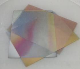
Déposition séléctive le rêve reviens
|
|
|
- Maximillian Barrett
- 5 years ago
- Views:
Transcription

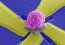
1 Willkommen Welcome Bienvenue Déposition séléctive le rêve reviens Patrik Hoffmann Michael Reinke, Yury Kuzminykh Ivo Utke, Carlos Guerra-Nunez, Ali Dabirian, Xavier Multone, Tristan Bret, Estelle Halary-Wagner, Giacomo Benvenuti,
2 Historical
3 What s new in ALD Top notch at Empa Si Si Precursor TTIP 1 Purge & Pump Precursor H 2 O 2 Purge & Pump t


4 Low Dimensional Materials Group Synthesis via charged particle beams, ALD, PVD Modelling e-beam induced Additive Manufacturing CNT Low-T ALD development ZnO / Al2O3 TiO 2 TiO2 / Y2O3 /SiO2 / Cu / MgF n m 5 1 / n m 5 n m Novel precursors for Ag and Ru 3D deposition (photonics) ALD Nucleation control on MW-CNTs [101] [011] 1 0 n m Oxide ALD multilayers on flexible polymers Hall sensors Telecom Laser Gratings AFM in SEM GIS in SEM PVD of model materials Combinatorial PVD & ALD


2)4 + 2H2O")
5 Atomic Layer Deposition of TiO2 TTIP Pulse Purge Ti(OCH(CH3)2)4 Self-limiting TiO2 60 C H H2O Pulse 1 cycle TiO2 Linear Growth Purge Ti(OCH(CH3)2)4 + 2H2O TiO2 + 4CH(CH3)2OH


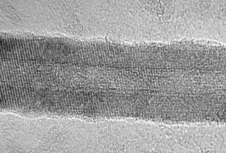
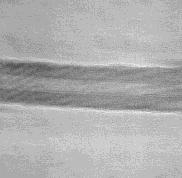
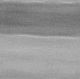
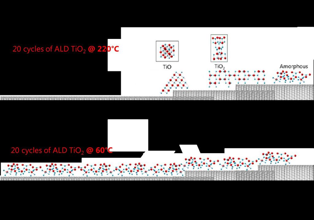
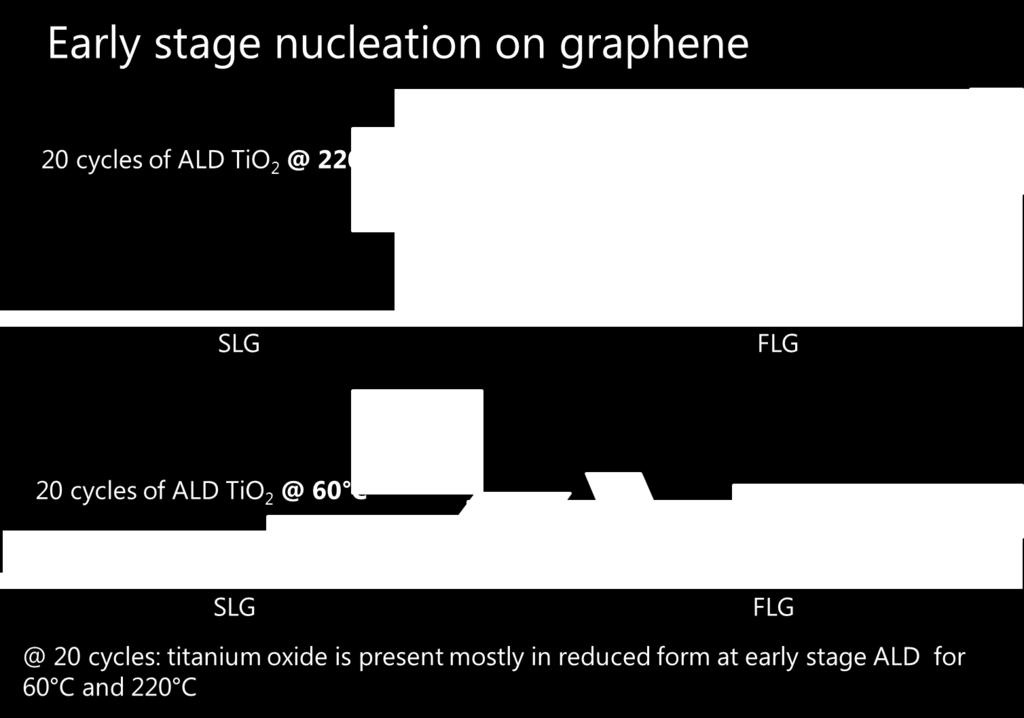
6 Early stage nucleation on SLG/FLG STEM at 80 kv Pristine sample 20 cycles of ALD TiO 2 SLG TiO2 60 C ALD TiO2 220 C ALD Areas of few 100 nm 2 of SLG FLG and a:c residues Fully covered by amorphous TiO2 -Anatase crystals 2 nm size the fewlayer graphene and contamination regions -Clean SLG pristine region largely free of nucleation. Y. Zhang, C. Guerra-Nunez et al. (2017): Atomic Layer Deposition of Titanium Oxide on Single Layer Graphene: an Atomic Scale Study towards Understanding Nucleation and Growth, Chemistry of Materials, DOI: /acs.chemmater.6b05143
7
8 A typical ALD process with two precursors Si Si Precursor TTIP 1 Purge & Pump Precursor H 2 O 2 Purge & Pump t growth process is driven by surface reactions no gas phase interactions
9 What happens if we change a bit? Si TTIP + H 2 O Pump, Pump, Pump growth process is driven by surface reactions no gas phase interactions
10 T T I P H 2 O Liquid N 2 Trap High Vacuum Chemical Vapor Deposition (HV-CVD) 10-6 mbar 4 inch substrate Inductive heater Liquid N 2 Trap No precursor interaction during precursor transport to the substrate Predictable (and controllable) precursor impinging rates Ring system with effusion sources Thermalyzed Precursor reservoir(s) Kuzminykh, et al., Surface and Coatings Technology, 2013,


11 Deposition of electro-optic thin films Team involved: Michael Reinke, Muriel Blum, Yury Kuzminykh, Patrik Hoffmann BaTiO 3 is a promising material for active electro-optic switches for integrated photonic circuits HV-CVD was used to deposit epitaxial barium titanate on buffered silicon at 400 C compatible with todays CMOS technology deposit substrate The electro-optic coefficient is currently optimized, highest values so far ~150pm/V Comparable to values of films grown by MBE at 600 C
 no film growth normal film growth we observe an initial incubation")
12 Film growth starts after an incubation period Analogue to conventional ALD, (almost) no film growth normal film growth we observe an initial incubation period
13 How to achieve selectivity? untreated Si treated Si TTIP + H 2 O Pump, Pump, Pump surface deactivation by pre-patterned self assembled monolayer

 Water contact angle on")

14 PTFS Patterning changes the surface chemistry OH OH OH OH OH OH CF 3 CF 3 CF 3 CF 3 CF 3 CF 3 CF 3 untreated Si treated Si 109 ± 2 PFTS (Perfluorodecyltrichlorosilane) Water contact angle on treated surface After PFTS treatment the surface is rendered hydrophobic e.g. the sticking coefficient for the precursors is decreased
15 Incubation Time Difference is Measured by Reflectometry Reflectometry Setup 1 Reflectometry Setup 2 untreated treated Incubation time on treated and untreated surfaces are measured simultaneously

16 Incubation Time Difference is Measured by Reflectometry selectivity window Reflectometry Setup 1 Reflectometry Setup 2 untreated treated Substrate: 225 C TTIP exposure: cm -2 s -1 H 2 O exposure: cm -2 s -1
17 The Incubation Time depends on the Precursor Dosage for the given TTIP dosage, the incubation time strongly depends on the H 2 O dosage
18 Selectivity depends on Incubation Time and Growth Rate The best selectivity is reached at high H 2 O and low TTIP dosages


 TiO 2")

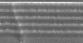
19 TiO 2 Growth is Surpressed on the Treated Surface Regions design of the pattern selective area deposition µm chessboard 2µm lines 2µm field spacing size 5µm TiO 2 nucleation sites as consequence of Overexposure during deposition Non perfect SAM layer Si (substrate) TiO 2 Substrate: 225 C TTIP exposure: cm -2 s -1 H 2 O exposure: cm -2 s -1 2 mm


20 Smaller Features are obtained by E-Beam Lithography chessboard 800nm chessboard 400nm chessboard 200nm 200nm patterning demonstrated, Grain size of the deposit determines the sidewall sharpness


 relevant for CVD and ALD")
21 Surface Kinetics Analysis of CVD and ALD Team involved: Michael Reinke, Evgeniy Ponomarev, Yury Kuzminykh, Patrik Hoffmann no. of added precursor molecules Analysis of surface kinetics is very challenging in conventional CVD and ALD techniques no. of incorporated precursor molecules Reaction probabilities HV-CVD allows precise control of precursor flux to the substrate; subsequent analysis reveals reaction probabilities CVD? Surface Kinetic parameters (activation energies) relevant for CVD and ALD can be extracted using a mathematical model to describe the deposition process ALD
22 Conclusions Selective growth is back! SAM s are rediscovered 0 nucleation sites remains a challenge No particle, no adatom, no defect allowed!!
TMT4320 Nanomaterials November 10 th, Thin films by physical/chemical methods (From chapter 24 and 25)
") 1 TMT4320 Nanomaterials November 10 th, 2015 Thin films by physical/chemical methods (From chapter 24 and 25) 2 Thin films by physical/chemical methods Vapor-phase growth (compared to liquid-phase growth)
1 TMT4320 Nanomaterials November 10 th, 2015 Thin films by physical/chemical methods (From chapter 24 and 25) 2 Thin films by physical/chemical methods Vapor-phase growth (compared to liquid-phase growth)
Graphene films on silicon carbide (SiC) wafers supplied by Nitride Crystals, Inc.
 wafers supplied by Nitride Crystals, Inc.") 9702 Gayton Road, Suite 320, Richmond, VA 23238, USA Phone: +1 (804) 709-6696 info@nitride-crystals.com www.nitride-crystals.com Graphene films on silicon carbide (SiC) wafers supplied by Nitride Crystals,
9702 Gayton Road, Suite 320, Richmond, VA 23238, USA Phone: +1 (804) 709-6696 info@nitride-crystals.com www.nitride-crystals.com Graphene films on silicon carbide (SiC) wafers supplied by Nitride Crystals,
Initial Stages of Growth of Organic Semiconductors on Graphene
 Initial Stages of Growth of Organic Semiconductors on Graphene Presented by: Manisha Chhikara Supervisor: Prof. Dr. Gvido Bratina University of Nova Gorica Outline Introduction to Graphene Fabrication
TiO2/sapphire Beam Splitter for High-order Harmonics
 Technical Communication TiO2/sapphire Beam Splitter for High-order Harmonics Y. Sanjo*1, M. Murata*1, Y. Tanaka*1, H. Kumagai*1, and M. Chigane*2 *1 Graduate School of Engineering,Osaka City University,
Harvesting Heat through Seebeck Spin Tunneling Effect
 Harvesting Heat through Seebeck Spin Tunneling Effect Costel Constantin James Madison University Science Enabled by Photon Source, May 2012 Outline 1. Spintronics vs. Spin Caloritronics. 2. Novel Spin
A. Optimizing the growth conditions of large-scale graphene films
 1 A. Optimizing the growth conditions of large-scale graphene films Figure S1. Optical microscope images of graphene films transferred on 300 nm SiO 2 /Si substrates. a, Images of the graphene films grown
Real-Time Chemical Sensing for Advanced Process Control in ALD
 Real-Time Chemical Sensing for Advanced Process Control in ALD Gary W. Rubloff 1, Laurent Henn-Lecordier 2, and Wei Lei 3 University of Maryland 1 Director, Maryland Center for Integrated Nano Science
Soft X-ray multilayer mirrors by ion assisted sputter deposition
 Soft X-ray multilayer mirrors by ion assisted sputter deposition Valentino Rigato INFN Laboratori Nazionali di Legnaro Bologna, September 21, 2010 Source: INFN-LNL-2009 V. RIGATO 1 SIF- Bologna September
Nanostructure. Materials Growth Characterization Fabrication. More see Waser, chapter 2
 Nanostructure Materials Growth Characterization Fabrication More see Waser, chapter 2 Materials growth - deposition deposition gas solid Physical Vapor Deposition Chemical Vapor Deposition Physical Vapor
Scaling up Chemical Vapor Deposition Graphene to 300 mm Si substrates
 Scaling up Chemical Vapor Deposition Graphene to 300 mm Si substrates Co- Authors Aixtron Alex Jouvray Simon Buttress Gavin Dodge Ken Teo The work shown here has received partial funding from the European
Subnanometre platinum clusters as highly active and selective catalysts for the oxidative dehydrogenation of propane
 DOI: 10.1038/NMAT2384 Subnanometre platinum clusters as highly active and selective catalysts for the oxidative dehydrogenation of propane Stefan Vajda, Larry A. Curtiss, Peter Zapol et al. Center for
Thin Film Bi-based Perovskites for High Energy Density Capacitor Applications
 ..SKELETON.. Thin Film Bi-based Perovskites for High Energy Density Capacitor Applications Colin Shear Advisor: Dr. Brady Gibbons 2010 Table of Contents Chapter 1 Introduction... 1 1.1 Motivation and Objective...
SUPPLEMENTARY INFORMATION
 SUPPLEMENTARY INFORMATION Facile Synthesis of High Quality Graphene Nanoribbons Liying Jiao, Xinran Wang, Georgi Diankov, Hailiang Wang & Hongjie Dai* Supplementary Information 1. Photograph of graphene
Film Deposition Part 1
 1 Film Deposition Part 1 Chapter 11 : Semiconductor Manufacturing Technology by M. Quirk & J. Serda Spring Semester 2013 Saroj Kumar Patra Semidonductor Manufacturing Technology, Norwegian University of
Supplementary Information Our InGaN/GaN multiple quantum wells (MQWs) based one-dimensional (1D) grating structures
 based one-dimensional (1D) grating structures") Polarized white light from hybrid organic/iii-nitrides grating structures M. Athanasiou, R. M. Smith, S. Ghataora and T. Wang* Department of Electronic and Electrical Engineering, University of Sheffield,
Polarized white light from hybrid organic/iii-nitrides grating structures M. Athanasiou, R. M. Smith, S. Ghataora and T. Wang* Department of Electronic and Electrical Engineering, University of Sheffield,
ESH Benign Processes for he Integration of Quantum Dots (QDs)
") ESH Benign Processes for he Integration of Quantum Dots (QDs) PIs: Karen K. Gleason, Department of Chemical Engineering, MIT Graduate Students: Chia-Hua Lee: PhD Candidate, Department of Material Science
ESH Benign Processes for he Integration of Quantum Dots (QDs) PIs: Karen K. Gleason, Department of Chemical Engineering, MIT Graduate Students: Chia-Hua Lee: PhD Candidate, Department of Material Science
In-situ Monitoring of Thin-Film Formation Processes by Spectroscopic Ellipsometry
 In-situ Monitoring of Thin-Film Formation Processes by Spectroscopic Ellipsometry Alexey Kovalgin Chair of Semiconductor Components MESA+ Institute for Nanotechnology Motivation Advantages of in-situ over
EE C245 ME C218 Introduction to MEMS Design Fall 2007
 EE C245 ME C218 Introduction to MEMS Design Fall 2007 Prof. Clark T.-C. Nguyen Dept. of Electrical Engineering & Computer Sciences University of California at Berkeley Berkeley, CA 94720 Lecture 4: Film
CURRENT STATUS OF NANOIMPRINT LITHOGRAPHY DEVELOPMENT IN CNMM
 U.S. -KOREA Forums on Nanotechnology 1 CURRENT STATUS OF NANOIMPRINT LITHOGRAPHY DEVELOPMENT IN CNMM February 17 th 2005 Eung-Sug Lee,Jun-Ho Jeong Korea Institute of Machinery & Materials U.S. -KOREA Forums
Carbon nanotubes synthesis. Ing. Eva Košťáková KNT, FT, TUL
 Carbon nanotubes synthesis Ing. Eva Košťáková KNT, FT, TUL Basic parameters: -Temperature (500, 1000 C ) -Pressure (normal, vacuum ) -Gas (ambient, inert atmosphere nitrogen, argon ) -Time (duration, time
Self-study problems and questions Processing and Device Technology, FFF110/FYSD13
 Self-study problems and questions Processing and Device Technology, FFF110/FYSD13 Version 2016_01 In addition to the problems discussed at the seminars and at the lectures, you can use this set of problems
High-density data storage: principle
 High-density data storage: principle Current approach High density 1 bit = many domains Information storage driven by domain wall shifts 1 bit = 1 magnetic nanoobject Single-domain needed Single easy axis
Supplementary Information. Atomic Layer Deposition of Platinum Catalysts on Nanowire Surfaces for Photoelectrochemical Water Reduction
 Supplementary Information Atomic Layer Deposition of Platinum Catalysts on Nanowire Surfaces for Photoelectrochemical Water Reduction Neil P. Dasgupta 1 ǂ, Chong Liu 1,2 ǂ, Sean Andrews 1,2, Fritz B. Prinz
Two-Dimensional (C 4 H 9 NH 3 ) 2 PbBr 4 Perovskite Crystals for. High-Performance Photodetector. Supporting Information for
 2 PbBr 4 Perovskite Crystals for. High-Performance Photodetector. Supporting Information for") Supporting Information for Two-Dimensional (C 4 H 9 NH 3 ) 2 PbBr 4 Perovskite Crystals for High-Performance Photodetector Zhenjun Tan,,ǁ, Yue Wu,ǁ, Hao Hong, Jianbo Yin, Jincan Zhang,, Li Lin, Mingzhan
Supporting Information for Two-Dimensional (C 4 H 9 NH 3 ) 2 PbBr 4 Perovskite Crystals for High-Performance Photodetector Zhenjun Tan,,ǁ, Yue Wu,ǁ, Hao Hong, Jianbo Yin, Jincan Zhang,, Li Lin, Mingzhan
Preparation of Nanostructures(Příprava Nanostruktur)
") Preparation of Nanostructures (Příprava Nanostruktur) jaroslav.hamrle@vsb.cz September 23, 2013 Outline 1 Introduction 2 Bulk crystal growth 3 Thin film preparation 4 Lateral structures 5 Surface plasma
Preparation of Nanostructures (Příprava Nanostruktur) jaroslav.hamrle@vsb.cz September 23, 2013 Outline 1 Introduction 2 Bulk crystal growth 3 Thin film preparation 4 Lateral structures 5 Surface plasma
Layer-modulated synthesis of uniform tungsten disulfide nanosheet using gas-phase precursors.
 Layer-modulated synthesis of uniform tungsten disulfide nanosheet using gas-phase precursors. Jusang Park * Hyungjun Kim School of Electrical and Electronics Engineering, Yonsei University, 262 Seongsanno,
Transparent Electrode Applications
 Transparent Electrode Applications LCD Solar Cells Touch Screen Indium Tin Oxide (ITO) Zinc Oxide (ZnO) - High conductivity - High transparency - Resistant to environmental effects - Rare material (Indium)
MSN551 LITHOGRAPHY II
 MSN551 Introduction to Micro and Nano Fabrication LITHOGRAPHY II E-Beam, Focused Ion Beam and Soft Lithography Why need electron beam lithography? Smaller features are required By electronics industry:
Engineered Flexible Conductive Barrier Films for Advanced Energy Devices
 The 13 th Korea-U.S. Forum on Nanotechnology Engineered Flexible Conductive Barrier Films for Advanced Energy Devices Jinsung Kwak 1, Yongsu Jo 1, Soon-Dong Park 2, Na Yeon Kim 1, Se-Yang Kim 1, Zonghoon
Atomic layer deposition of titanium nitride
 Atomic layer deposition of titanium nitride Jue Yue,version4, 04/26/2015 Introduction Titanium nitride is a hard and metallic material which has found many applications, e.g.as a wear resistant coating[1],
Repetition: Ion Plating
 Repetition: Ion Plating Substrate HV (bis ca. 1kV) Optional ionization system Source Ionized filling gas Source material, ionized or neutral Repetition: Ion Plating Ion Species Separated ion source Ions
Chemical Vapor Deposition (CVD)
") Chemical Vapor Deposition (CVD) source chemical reaction film substrate More conformal deposition vs. PVD t Shown here is 100% conformal deposition ( higher temp has higher surface diffusion) t step 1
Chemical Vapor Deposition (CVD) source chemical reaction film substrate More conformal deposition vs. PVD t Shown here is 100% conformal deposition ( higher temp has higher surface diffusion) t step 1
Chapter 2 Synthesis, Structure, and Properties of Graphene and Graphene Oxide
 Chapter 2 Synthesis, Structure, and Properties of Graphene and Graphene Oxide 2.1 Introduction To develop large-area graphene-based TCFs, one of the foremost challenges is to produce sufficient amounts
Plasma Deposition (Overview) Lecture 1
 Lecture 1") Plasma Deposition (Overview) Lecture 1 Material Processes Plasma Processing Plasma-assisted Deposition Implantation Surface Modification Development of Plasma-based processing Microelectronics needs (fabrication
Plasma Deposition (Overview) Lecture 1 Material Processes Plasma Processing Plasma-assisted Deposition Implantation Surface Modification Development of Plasma-based processing Microelectronics needs (fabrication
Investigation of graphene layer application to RF-grade copper surfaces
 Investigation of graphene layer application to RF-grade copper surfaces Alex Murokh RadiaBeam Technologies, LLC. SLAC National Accelerator Laboratory, February 10, 2011 Motivation High gradient research
Fundamental insight into ALD processing by in-
 Fakultät Elektrotechnik und Informationstechnik Institut für Halbleiter- und Mikrosystemtechnik Fundamental insight into ALD processing by in- situ observation Johann W. Bartha M. Albert, M. Junige and
Complex Nanostructures by Atomic Layer Deposition. Kornelius Nielsch.
 Complex Nanostructures by Atomic Layer Deposition Kornelius Nielsch Institute of Applied Physics, University of Hamburg (Germany) knielsch@physnet.uni-hamburg.de Outline History and Principle Ferromagnetic
Modern Methods in Heterogeneous Catalysis Research: Preparation of Model Systems by Physical Methods
 Modern Methods in Heterogeneous Catalysis Research: Preparation of Model Systems by Physical Methods Methods for catalyst preparation Methods discussed in this lecture Physical vapour deposition - PLD
Supplementary Figure 1 Experimental setup for crystal growth. Schematic drawing of the experimental setup for C 8 -BTBT crystal growth.
 Supplementary Figure 1 Experimental setup for crystal growth. Schematic drawing of the experimental setup for C 8 -BTBT crystal growth. Supplementary Figure 2 AFM study of the C 8 -BTBT crystal growth
EE C245 ME C218 Introduction to MEMS Design Fall 2007
 EE C245 ME C218 Introduction to MEMS Design Fall 2007 Prof. Clark T.-C. Nguyen Dept. of Electrical Engineering & Computer Sciences University of California at Berkeley Berkeley, CA 94720 Lecture 5: ALD,
High-resolution Characterization of Organic Ultrathin Films Using Atomic Force Microscopy
 High-resolution Characterization of Organic Ultrathin Films Using Atomic Force Microscopy Jing-jiang Yu Nanotechnology Measurements Division Agilent Technologies, Inc. Atomic Force Microscopy High-Resolution
Wafer-scale fabrication of graphene
 Wafer-scale fabrication of graphene Sten Vollebregt, MSc Delft University of Technology, Delft Institute of Mircosystems and Nanotechnology Delft University of Technology Challenge the future Delft University
OPTI510R: Photonics. Khanh Kieu College of Optical Sciences, University of Arizona Meinel building R.626
 OPTI510R: Photonics Khanh Kieu College of Optical Sciences, University of Arizona kkieu@optics.arizona.edu Meinel building R.626 Announcements HW#3 is assigned due Feb. 20 st Mid-term exam Feb 27, 2PM
Supplementary Information
 Electronic Supplementary Material (ESI) for Physical Chemistry Chemical Physics. This journal is the Owner Societies 2015 Supplementary Information Vertical Heterostructures of MoS2 and Graphene Nanoribbons
Supporting Information
 Supporting Information Repeated Growth Etching Regrowth for Large-Area Defect-Free Single-Crystal Graphene by Chemical Vapor Deposition Teng Ma, 1 Wencai Ren, 1 * Zhibo Liu, 1 Le Huang, 2 Lai-Peng Ma,
ALD & ALE Tutorial Speakers and Schedule
 ALD & ALE Tutorial Speakers and Schedule Sunday, July 29, 2018 1:00-1:05 Tutorial Welcome 1:05-1:50 1:50-2:35 2:35-3:20 Challenges of ALD Applications in Memory Semiconductor Devices, Choon Hwan Kim (SK
The goal of this project is to enhance the power density and lowtemperature efficiency of solid oxide fuel cells (SOFC) manufactured by atomic layer
 manufactured by atomic layer") Stanford University Michael Shandalov1, Shriram Ramanathan2, Changhyun Ko2 and Paul McIntyre1 1Department of Materials Science and Engineering, Stanford University 2Division of Engineering and Applied
Stanford University Michael Shandalov1, Shriram Ramanathan2, Changhyun Ko2 and Paul McIntyre1 1Department of Materials Science and Engineering, Stanford University 2Division of Engineering and Applied
Fiducial Marks for EUV mask blanks. Jan-Peter Urbach, James Folta, Cindy Larson, P.A. Kearney, and Thomas White
 Fiducial Marks for EUV mask blanks Jan-Peter Urbach, James Folta, Cindy Larson, P.A. Kearney, and Thomas White Fiducial marks are laser scribed on 200 mm wafers to enable defect registration on metrology
EE143 Fall 2016 Microfabrication Technologies. Lecture 6: Thin Film Deposition Reading: Jaeger Chapter 6
 EE143 Fall 2016 Microfabrication Technologies Lecture 6: Thin Film Deposition Reading: Jaeger Chapter 6 Prof. Ming C. Wu wu@eecs.berkeley.edu 511 Sutardja Dai Hall (SDH) 1 Vacuum Basics Units 1 atmosphere
Supporting Information. Fast Synthesis of High-Performance Graphene by Rapid Thermal Chemical Vapor Deposition
 1 Supporting Information Fast Synthesis of High-Performance Graphene by Rapid Thermal Chemical Vapor Deposition Jaechul Ryu, 1,2, Youngsoo Kim, 4, Dongkwan Won, 1 Nayoung Kim, 1 Jin Sung Park, 1 Eun-Kyu
Lecture 30: Kinetics of Epitaxial Growth: Surface Diffusion and
 Lecture 30: Kinetics of Epitaxial Growth: Surface Diffusion and Nucleation Today s topics Understanding the basics of epitaxial techniques used for surface growth of crystalline structures (films, or layers).
JOHN G. EKERDT RESEARCH FOCUS
 JOHN G. EKERDT RESEARCH FOCUS We study the surface, growth and materials chemistry of ultrathin metal and dielectric films. Our work seeks to: 1) develop and understand the reactions and chemistry that
VACUUM TECHNOLOGIES NEEDED FOR 3D DEVICE PROCESSING
 VACUUM TECHNOLOGIES NEEDED FOR 3D DEVICE PROCESSING Future ICs will use more 3D device structures such as finfets and gate-all-around (GAA) transistors, and so vacuum deposition processes are needed that
Nova 600 NanoLab Dual beam Focused Ion Beam IITKanpur
 Nova 600 NanoLab Dual beam Focused Ion Beam system @ IITKanpur Dual Beam Nova 600 Nano Lab From FEI company (Dual Beam = SEM + FIB) SEM: The Electron Beam for SEM Field Emission Electron Gun Energy : 500
Surface and Interface Characterization of Polymer Films
 Surface and Interface Characterization of Polymer Films Jeff Shallenberger, Evans Analytical Group 104 Windsor Center Dr., East Windsor NJ Copyright 2013 Evans Analytical Group Outline Introduction to
Repetition: Practical Aspects
 Repetition: Practical Aspects Reduction of the Cathode Dark Space! E x 0 Geometric limit of the extension of a sputter plant. Lowest distance between target and substrate V Cathode (Target/Source) - +
Deposition of polymeric thin films by PVD process. Hachet Dorian 09/03/2016
 Deposition of polymeric thin films by PVD process Hachet Dorian 09/03/2016 Polymeric Thin Films nowadays The evaporation of polymers Ionization-Assisted Method Vacuum deposition 0,055eV/molecule at 1000
Supplementary Information for. Origin of New Broad Raman D and G Peaks in Annealed Graphene
 Supplementary Information for Origin of New Broad Raman D and G Peaks in Annealed Graphene Jinpyo Hong, Min Kyu Park, Eun Jung Lee, DaeEung Lee, Dong Seok Hwang and Sunmin Ryu* Department of Applied Chemistry,
DEPOSITION OF THIN TiO 2 FILMS BY DC MAGNETRON SPUTTERING METHOD
 Chapter 4 DEPOSITION OF THIN TiO 2 FILMS BY DC MAGNETRON SPUTTERING METHOD 4.1 INTRODUCTION Sputter deposition process is another old technique being used in modern semiconductor industries. Sputtering
Nanoparticle Devices. S. A. Campbell, ECE C. B. Carter, CEMS H. Jacobs, ECE J. Kakalios, Phys. U. Kortshagen, ME. Institute of Technology
 Nanoparticle Devices S. A. Campbell, ECE C. B. Carter, CEMS H. Jacobs, ECE J. Kakalios, Phys. U. Kortshagen, ME Applications of nanoparticles Flash Memory Tiwari et al., Appl. Phys. Lett. 68, 1377, 1996.
Alternative deposition solution for cost reduction of TSV integration
 Alternative deposition solution for cost reduction of TSV integration J. Vitiello, F. Piallat, L. Bonnet KOBUS 611 rue Aristide Bergès, Z.A. de Pré Millet, Montbonnot-Saint-Martin, 38330 France Ph: +33
The design of an integrated XPS/Raman spectroscopy instrument for co-incident analysis
 The design of an integrated XPS/Raman spectroscopy instrument for co-incident analysis Tim Nunney The world leader in serving science 2 XPS Surface Analysis XPS +... UV Photoelectron Spectroscopy UPS He(I)
Figure 1: Graphene release, transfer and stacking processes. The graphene stacking began with CVD
 Supplementary figure 1 Graphene Growth and Transfer Graphene PMMA FeCl 3 DI water Copper foil CVD growth Back side etch PMMA coating Copper etch in 0.25M FeCl 3 DI water rinse 1 st transfer DI water 1:10
High speed vacuum deposition of organic TFTs in a roll-to-roll facility
 High speed vacuum deposition of organic TFTs in a roll-to-roll facility Dr Hazel Assender University of Oxford 1 Prof Martin Taylor Eifion Patchett, Aled Williams Prof Long Lin Prof Steve Yeates Dr John
Agenda. 1. Atomic Layer Deposition Technology
 Agenda 1. Atomic Layer Deposition Technology 2. What is ALD? Atomic Layer Deposition is invented in 1977 by T. Suntola et al. - New Deposition Method for Electro-Luminescent Display (ZnS:Mn Thin Films)
Low Voltage Field Emission SEM (LV FE-SEM): A Promising Imaging Approach for Graphene Samples
: A Promising Imaging Approach for Graphene Samples") Low Voltage Field Emission SEM (LV FE-SEM): A Promising Imaging Approach for Graphene Samples Jining Xie Agilent Technologies May 23 rd, 2012 www.agilent.com/find/nano Outline 1. Introduction 2. Agilent
Low Voltage Field Emission SEM (LV FE-SEM): A Promising Imaging Approach for Graphene Samples Jining Xie Agilent Technologies May 23 rd, 2012 www.agilent.com/find/nano Outline 1. Introduction 2. Agilent
GRAPHENE ON THE Si-FACE OF SILICON CARBIDE USER MANUAL
 GRAPHENE ON THE Si-FACE OF SILICON CARBIDE USER MANUAL 1. INTRODUCTION Silicon Carbide (SiC) is a wide band gap semiconductor that exists in different polytypes. The substrate used for the fabrication
An account of our efforts towards air quality monitoring in epitaxial graphene on SiC
 European Network on New Sensing Technologies for Air Pollution Control and Environmental Sustainability - EuNetAir COST Action TD1105 2 nd International Workshop EuNetAir on New Sensing Technologies for
UNIVERSITY OF CALIFORNIA College of Engineering Department of Electrical Engineering and Computer Sciences. Fall Exam 1
 UNIVERSITY OF CALIFORNIA College of Engineering Department of Electrical Engineering and Computer Sciences EECS 143 Fall 2008 Exam 1 Professor Ali Javey Answer Key Name: SID: 1337 Closed book. One sheet
Top down and bottom up fabrication
 Lecture 24 Top down and bottom up fabrication Lithography ( lithos stone / graphein to write) City of words lithograph h (Vito Acconci, 1999) 1930 s lithography press Photolithography d 2( NA) NA=numerical
Low temperature atomic layer deposition of cobalt oxide as an effective catalyst for photoelectrochemical water splitting devices
 Low temperature atomic layer deposition of cobalt oxide as an effective catalyst for photoelectrochemical water splitting devices Jiyeon Kim, a Tomi Iivonen, b Jani Hämäläinen, b Marianna Kemell, b Kristoffer
SUPPLEMENTARY INFORMATION
 Direct Visualization of Large-Area Graphene Domains and Boundaries by Optical Birefringency Dae Woo Kim 1,*, Yun Ho Kim 1,2,*, Hyeon Su Jeong 1, Hee-Tae Jung 1 * These authors contributed equally to this
Supporting Information
 Supporting Information Improved Stability of Atomic Layer Deposited Amorphous TiO 2 Photoelectrode Coatings by Thermally Induced Oxygen Defects Markku Hannula, Harri Ali-Löytty, Kimmo Lahtonen, Essi Sarlin,
Etching: Basic Terminology
 Lecture 7 Etching Etching: Basic Terminology Introduction : Etching of thin films and sometimes the silicon substrate are very common process steps. Usually selectivity, and directionality are the first
Regents of the University of California
 Deep Reactive-Ion Etching (DRIE) DRIE Issues: Etch Rate Variance The Bosch process: Inductively-coupled plasma Etch Rate: 1.5-4 μm/min Two main cycles in the etch: Etch cycle (5-15 s): SF 6 (SF x+ ) etches
Step Coverage by ALD Films: Theory and Examples
 Step Coverage by ALD Films: Theory and Examples of Ideal and Non-Ideal Reactions Roy G. Gordon Cambridge, MA 1 L Step Coverage in Holes with High Aspect Ratio Step coverage = (b/a) x 100% a Aspect ratio
Vapor-Phase Cutting of Carbon Nanotubes Using a Nanomanipulator Platform
 Vapor-Phase Cutting of Carbon Nanotubes Using a Nanomanipulator Platform MS&T 10, October 18, 2010 Vladimir Mancevski, President and CTO, Xidex Corporation Philip D. Rack, Professor, The University of
Supplementary Materials
 Atomic layer-deposited tunnel oxide stabilizes silicon photoanodes for water oxidation Yi Wei Chen 1, Jonathan D. Prange 2, Simon Dühnen 2, Yohan Park 1, Marika Gunji 1, Christopher E. D. Chidsey 2, and
Vacuum Technology and film growth. Diffusion Resistor
 Vacuum Technology and film growth Poly Gate pmos Polycrystaline Silicon Source Gate p-channel Metal-Oxide-Semiconductor (MOSFET) Drain polysilicon n-si ion-implanted Diffusion Resistor Poly Si Resistor
Graphene Fundamentals and Emergent Applications
 Graphene Fundamentals and Emergent Applications Jamie H. Warner Department of Materials University of Oxford Oxford, UK Franziska Schaffel Department of Materials University of Oxford Oxford, UK Alicja
Supplementary Figure 1 XRD pattern of a defective TiO 2 thin film deposited on an FTO/glass substrate, along with an XRD pattern of bare FTO/glass
 Supplementary Figure 1 XRD pattern of a defective TiO 2 thin film deposited on an FTO/glass substrate, along with an XRD pattern of bare FTO/glass and a reference pattern of anatase TiO 2 (JSPDS No.: 21-1272).
What are Carbon Nanotubes? What are they good for? Why are we interested in them?
 Growth and Properties of Multiwalled Carbon Nanotubes What are Carbon Nanotubes? What are they good for? Why are we interested in them? - Interconnects of the future? - our vision Where do we stand - our
Nanocarbon Technology for Development of Innovative Devices
 Nanocarbon Technology for Development of Innovative Devices Shintaro Sato Daiyu Kondo Shinichi Hirose Junichi Yamaguchi Graphene, a one-atom-thick honeycomb lattice made of carbon, and a carbon nanotube,
Graphene: Plane and Simple Electrical Metrology?
 Graphene: Plane and Simple Electrical Metrology? R. E. Elmquist, F. L. Hernandez-Marquez, M. Real, T. Shen, D. B. Newell, C. J. Jacob, and G. R. Jones, Jr. National Institute of Standards and Technology,
One-Step Combustion Synthesis of Carbon-Coated Nanoparticles using Multiple-Diffusion Flames
 Paper # 070HE-0031 Topic: Heterogeneous Combustion, Sprays & Droplets 8 th U. S. National Combustion Meeting Organized by the Western States Section of the Combustion Institute and hosted by the University
LOW-TEMPERATURE Si (111) HOMOEPITAXY AND DOPING MEDIATED BY A MONOLAYER OF Pb
 HOMOEPITAXY AND DOPING MEDIATED BY A MONOLAYER OF Pb") LOW-TEMPERATURE Si (111) HOMOEPITAXY AND DOPING MEDIATED BY A MONOLAYER OF Pb O.D. DUBON, P.G. EVANS, J.F. CHERVINSKY, F. SPAEPEN, M.J. AZIZ, and J.A. GOLOVCHENKO Division of Engineering and Applied Sciences,
LOW-TEMPERATURE Si (111) HOMOEPITAXY AND DOPING MEDIATED BY A MONOLAYER OF Pb O.D. DUBON, P.G. EVANS, J.F. CHERVINSKY, F. SPAEPEN, M.J. AZIZ, and J.A. GOLOVCHENKO Division of Engineering and Applied Sciences,
Introducing the RoVaCBE Flagship project: Roll-to-roll Vacuum-processed Carbon Based Electronics. Dr Hazel Assender, University of Oxford
 Introducing the RoVaCBE Flagship project: Roll-to-roll Vacuum-processed Carbon Based Electronics Dr Hazel Assender, University of Oxford DALMATIAN TECHNOLOGY 21 st Sept 2010 1 Organic electronics Opportunity
ULTRA-SHORT OPTICAL PULSE GENERATION WITH SINGLE-LAYER GRAPHENE
 Journal of Nonlinear Optical Physics & Materials Vol. 19, No. 4 (2010) 767 771 c World Scientific Publishing Company DOI: 10.1142/S021886351000573X ULTRA-SHORT OPTICAL PULSE GENERATION WITH SINGLE-LAYER
ALD Nucleation and Area-Selective Deposition
 ALD Nucleation and Area-Selective Deposition Prof Gregory N. Parsons Department of Chemical and Biomolecular Engineering North Carolina State University Raleigh North Carolina USA 1 Outline 1. Nucleation
Novel Tooling for Scaling of High Quality CVD Graphene Production. Karlheinz Strobl, Mathieu Monville, Riju Singhal and Samuel Wright
 Novel Tooling for Scaling of High Quality CVD Graphene Production Karlheinz Strobl, Mathieu Monville, Riju Singhal and Samuel Wright 1 Commercialization of Nano Materials Commercialization Volume production
Toward Clean Suspended CVD Graphene
 Electronic Supplementary Material (ESI) for RSC Advances. This journal is The Royal Society of Chemistry 2016 Supplemental information for Toward Clean Suspended CVD Graphene Alexander Yulaev 1,2,3, Guangjun
TRANSVERSE SPIN TRANSPORT IN GRAPHENE
 International Journal of Modern Physics B Vol. 23, Nos. 12 & 13 (2009) 2641 2646 World Scientific Publishing Company TRANSVERSE SPIN TRANSPORT IN GRAPHENE TARIQ M. G. MOHIUDDIN, A. A. ZHUKOV, D. C. ELIAS,
Fabrication at the nanoscale for nanophotonics
 Fabrication at the nanoscale for nanophotonics Ilya Sychugov, KTH Materials Physics, Kista silicon nanocrystal by electron beam induced deposition lithography Outline of basic nanofabrication methods Devices
Atmospheric pressure Plasma Enhanced CVD for large area deposition of TiO 2-x electron transport layers for PV. Heather M. Yates
 Atmospheric pressure Plasma Enhanced CVD for large area deposition of TiO 2-x electron transport layers for PV Heather M. Yates Why the interest? Perovskite solar cells have shown considerable promise
Raman spectroscopy study of rotated double-layer graphene: misorientation angle dependence of electronic structure
 Supplementary Material for Raman spectroscopy study of rotated double-layer graphene: misorientation angle dependence of electronic structure Kwanpyo Kim 1,2,3, Sinisa Coh 1,3, Liang Z. Tan 1,3, William
Plasmonic sensing of heat transport and phase change near solid-liquid interfaces
 Plasmonic sensing of heat transport and phase change near solid-liquid interfaces David G. Cahill and Jonglo Park Department of Materials Science and Engineering University of Illinois at Urbana-Champaign
CVD: General considerations.
 CVD: General considerations. PVD: Move material from bulk to thin film form. Limited primarily to metals or simple materials. Limited by thermal stability/vapor pressure considerations. Typically requires
There's Plenty of Room at the Bottom
 There's Plenty of Room at the Bottom 12/29/1959 Feynman asked why not put the entire Encyclopedia Britannica (24 volumes) on a pin head (requires atomic scale recording). He proposed to use electron microscope
File name: Supplementary Information Description: Supplementary Figures, Supplementary Notes, Supplementary Tables, Supplementary References
 File name: Supplementary Information Description: Supplementary Figures, Supplementary Notes, Supplementary Tables, Supplementary References Supplementary Figure 1 Illustration of the reaction chamber
Fabrication of ordered array at a nanoscopic level: context
 Fabrication of ordered array at a nanoscopic level: context Top-down method Bottom-up method Classical lithography techniques Fast processes Size limitations it ti E-beam techniques Small sizes Slow processes