Chemical Vapor Deposition (CVD)
|
|
|
- Albert Stevens
- 6 years ago
- Views:
Transcription
1 Chemical Vapor Deposition (CVD) source chemical reaction film substrate More conformal deposition vs. PVD t Shown here is 100% conformal deposition ( higher temp has higher surface diffusion) t step 1
2 (a)sio2 gas solid LPCVD Examples SiH 4 O2 SiO2 2 H 2 gas 350oC-500oC (b)psg : phospho silicate glass. P2O5 SiO2 4 PH 3 5O2 2 P2O5 6 H 2 SiH 4 O2 SiO2 2 H 2 350oC-500oC (c)teos :tetraethylene orthosilicate. Si OC2 H 5 4 SiO2 C X H Y OZ 2
3 ( d ) Si 3 N 3 SiH 4 ( e ) Poly 4 NH 3 Si 3 N 4 12 H 2 Si 600 o C SiH 4 Si 2 H 2 ( f )W WF 6 3 H 2 W 6 HF 3

4 CVD Reactors 4
5 CVD Mechanisms reactant surface diffusion 3 stagnant gas layer 4 substrate 1 = Diffusion of reactant to surface 2 = Absorption of reactant to surface 3 = Chemical reaction 4 = Desorption of gas by-products 5 = Outdiffusion of by-product gas 5
6 Example: Poly-Si Deposition 6
7 CVD Growth Rate Model Flux across boundary F1 h G (CG CS ) Flux used in reaction F2 k S CS Normalize to total pressure Y CGAS CALL _ SPECIES F Thickness growth velocity v N PGAS PGAS _ 1 PGAS _ 2... N = atomic density of film 7
8 Diffusion Constant in Gas T3 / 2 D Do P n1 v n2 v v dn Proof: F = 4-4 = 4 ( dx) where = mean free path of gas collision. v dn F=D D= dx 2 kt Since and v T P D T3/2/P
9 Mathematical Model for CVD (Cont.) Transport parameter hg = D/ D = gas diffusion constant = Do T 3/2 / Pressure Surface reaction parameter ks = koexp (-Ea/kT) Balancing F1=F2 Growth velocity CALL _ SPECIES F 1 v Y N (1 / k S 1 / hg ) N CALL_SPECIES = concentration at top of boundary layer N =atomic density of deposited material Limiting cases ks << hg Surface Reaction limited hg << ks Mass Transport limited 9
10 Deposition Rate versus Temp [log scale] Rate 3 2 Mass transport limited R T surface-reaction limited R e EA / kt 1/ T 0 high T low T 10
11 11
12 Boundary Layer Thickness vs. Distance x U S ( x) 1 2 = viscosity, = density, U = velocity *See handout on CVD Kinetics for derivation 12
13 Average Boundary Layer thickness < > 1 L 2 ( x) dx L 0 3 UL Re L UL is called the Reynold Number of the reactor. When Re is small ( < 2000), gas flow is viscous. When Re is large (>2000), gas flow is turbulent which is undesirable. If deposition rate is mass transfer limited, 1 R hg U 13
14 Growth Rate Dependence on Flow Velocity Fixed temp T CALL _ SPECIES F 1 v Y N (1 / k S 1 / hg ) N 14
 15")
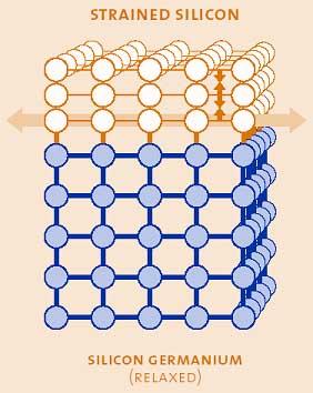
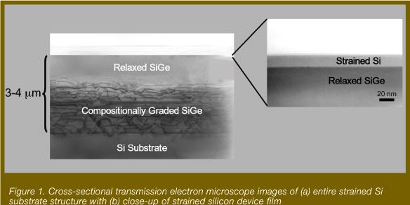
15 LPCVD Reactors (next page) 15
16 LPCVD: Low Pressure and high gas velocity due to pumping hg Example calculation: P reduces ~1000X from 1 atmosphere to ~1 Torr Velocity of gas flow U increases ~100X due to pumping D 1 P From 760Torr 1Torr D 1000X U 1000 ~ 3X = 100 velocity of gas flow 100X Gas density P hg D X 3 Therefore, LPCVD is more likely to be surface reaction limited 16
17 LPCVD Features (1) R, since hg (2) More conformal deposition, if T is uniform Wafer topography (3) Inter-wafer and intra-wafer thickness uniformity less sensitive to gas flow patterns. (i.e. wafer placement). 17
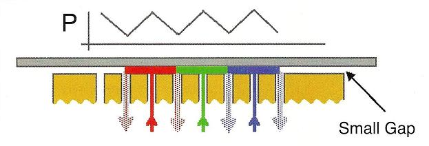
18 Gas Flow Issues (1) depends on gas flow pattern Furnace tube wafers (2) Mass depletion problem in more less out 18
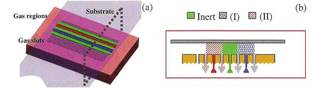
19 Solutions for mass depletion problem (1) Temperature Ramping along reactor length For reaction - limited regime: R(x) = A exp[-ea/kt] C(x) [where C(x) = SiH4 Conc.] Creating a temperature gradient of C along the tube will give better uniformity. (2) Distributed Feed Reactors 19

20 PECVD Reactors 20
21 Plasma Enhanced CVD Ionized chemical species allows a lower process temperature to be used. Film properties (e.g. mechanical stress) can be tailored by controllable ion bombardment with substrate bias voltage. 21
22 Epitaxial Growth Processing Temperature oC Requires an ultra-clean Si surface prior to epi growth. Requires deposition of Si at very high temperature for perfect crystallinity. 22

23 Strained Si Growth by Heteroepitaxy 23

24 Principle of Atomic Layer Deposition Self-limiting surface reactions of suitable precursor compounds A and B, which form the desired product S in a binary reaction cycle consisting of two sequential half-reactions. For an extensive list of precursors, see Ritala and Leskela, Handook of Thin Film Materials, Vol.1, Chap 2 (2002) 24

25 Timing Sequence : CVD vs ALD 25


26 Spatial ALD Reaction Chamber A Reaction Chamber B The reactor has separate zones exposing the precursors one by one to a substrate that moves underneath the reactor. Gas bearings between the zones eliminate cross-diffusion and therefore the need for purge steps. Half-reaction timescales are ~10 msec, enabling ultrahigh deposition rates while maintaining ALD film quality. Source: PV Society,

27 Possible Spatial ALD Configuration 27

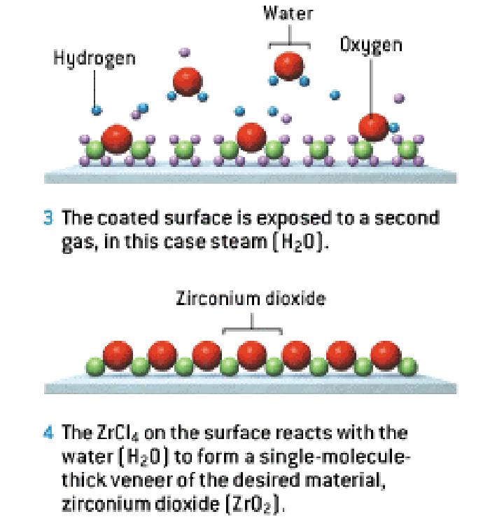
28 Example: ZrO2 ALD 28

29 Step Coverage (Al2O3) 29
30 SUMMARY OF THIN FILM MODULE Vacuum Basics Mean Free Path and Impingement Rate Plasma Basics - A plasma sheath above electrode surface which maintains a voltage drop ( -10 to V) for ion bombardment PVD and CVD Evaporation Vapor Pressure Sputtering Deposition- Sputtering Yield, Co-sputtering PVD Issues thickness uniformity across wafer, Step Coverage ( geometric shadowing, Self Shadowing) CVD Deposition Rate ( hg versus ks effects) CVD Issues Conformal coverage, Mass depletion Plasma Enhanced CVD (PECVD) - qualitative Epitaxial Growth - qualitative Atomic Layer Deposition (ALD) - qualitative 30
EE143 Fall 2016 Microfabrication Technologies. Lecture 6: Thin Film Deposition Reading: Jaeger Chapter 6
 EE143 Fall 2016 Microfabrication Technologies Lecture 6: Thin Film Deposition Reading: Jaeger Chapter 6 Prof. Ming C. Wu wu@eecs.berkeley.edu 511 Sutardja Dai Hall (SDH) 1 Vacuum Basics Units 1 atmosphere
Section 5: Thin Film Deposition part 1 : sputtering and evaporation. Jaeger Chapter 6. EE143 Ali Javey
 Section 5: Thin Film Deposition part 1 : sputtering and evaporation Jaeger Chapter 6 Vacuum Basics 1. Units 1 atmosphere = 760 torr = 1.013x10 5 Pa 1 bar = 10 5 Pa = 750 torr 1 torr = 1 mm Hg 1 mtorr =
EE C245 ME C218 Introduction to MEMS Design Fall 2007
 EE C245 ME C218 Introduction to MEMS Design Fall 2007 Prof. Clark T.-C. Nguyen Dept. of Electrical Engineering & Computer Sciences University of California at Berkeley Berkeley, CA 94720 Lecture 4: Film
Thin Film Deposition. Reading Assignments: Plummer, Chap 9.1~9.4
 Thin Film Deposition Reading Assignments: Plummer, Chap 9.1~9.4 Thermally grown Deposition Thin Film Formation Thermally grown SiO 2 Deposition SiO 2 Oxygen is from gas phase Silicon from substrate Oxide
Film Deposition Part 1
 1 Film Deposition Part 1 Chapter 11 : Semiconductor Manufacturing Technology by M. Quirk & J. Serda Spring Semester 2013 Saroj Kumar Patra Semidonductor Manufacturing Technology, Norwegian University of
Modern Methods in Heterogeneous Catalysis Research: Preparation of Model Systems by Physical Methods
 Modern Methods in Heterogeneous Catalysis Research: Preparation of Model Systems by Physical Methods Methods for catalyst preparation Methods discussed in this lecture Physical vapour deposition - PLD
UNIVERSITY OF CALIFORNIA. College of Engineering. Department of Electrical Engineering and Computer Sciences. Professor Ali Javey.
 UNIVERSITY OF CALIFORNIA College of Engineering Department of Electrical Engineering and Computer Sciences EE 143 Professor Ali Javey Spring 2009 Exam 2 Name: SID: Closed book. One sheet of notes is allowed.
CVD: General considerations.
 CVD: General considerations. PVD: Move material from bulk to thin film form. Limited primarily to metals or simple materials. Limited by thermal stability/vapor pressure considerations. Typically requires
Semiconductor Technology
 Semiconductor Technology from A to Z Deposition www.halbleiter.org Contents Contents List of Figures II 1 Deposition 1 1.1 Plasma, the fourth aggregation state of a material............. 1 1.1.1 Plasma
Vacuum Technology and film growth. Diffusion Resistor
 Vacuum Technology and film growth Poly Gate pmos Polycrystaline Silicon Source Gate p-channel Metal-Oxide-Semiconductor (MOSFET) Drain polysilicon n-si ion-implanted Diffusion Resistor Poly Si Resistor
Introduction to Thin Film Processing
 Introduction to Thin Film Processing Deposition Methods Many diverse techniques available Typically based on three different methods for providing a flux of atomic or molecular material Evaporation Sputtering
TMT4320 Nanomaterials November 10 th, Thin films by physical/chemical methods (From chapter 24 and 25)
") 1 TMT4320 Nanomaterials November 10 th, 2015 Thin films by physical/chemical methods (From chapter 24 and 25) 2 Thin films by physical/chemical methods Vapor-phase growth (compared to liquid-phase growth)
1 TMT4320 Nanomaterials November 10 th, 2015 Thin films by physical/chemical methods (From chapter 24 and 25) 2 Thin films by physical/chemical methods Vapor-phase growth (compared to liquid-phase growth)
Repetition: Practical Aspects
 Repetition: Practical Aspects Reduction of the Cathode Dark Space! E x 0 Geometric limit of the extension of a sputter plant. Lowest distance between target and substrate V Cathode (Target/Source) - +
Agenda. 1. Atomic Layer Deposition Technology
 Agenda 1. Atomic Layer Deposition Technology 2. What is ALD? Atomic Layer Deposition is invented in 1977 by T. Suntola et al. - New Deposition Method for Electro-Luminescent Display (ZnS:Mn Thin Films)
Fabrication Technology, Part I
 EEL5225: Principles of MEMS Transducers (Fall 2004) Fabrication Technology, Part I Agenda: Microfabrication Overview Basic semiconductor devices Materials Key processes Oxidation Thin-film Deposition Reading:
Reactive Ion Etching (RIE)
") Reactive Ion Etching (RIE) RF 13.56 ~ MHz plasma Parallel-Plate Reactor wafers Sputtering Plasma generates (1) Ions (2) Activated neutrals Enhance chemical reaction 1 2 Remote Plasma Reactors Plasma Sources
Reactive Ion Etching (RIE) RF 13.56 ~ MHz plasma Parallel-Plate Reactor wafers Sputtering Plasma generates (1) Ions (2) Activated neutrals Enhance chemical reaction 1 2 Remote Plasma Reactors Plasma Sources
Dynamic Equipment and Process Simulation for Atomic Layer Deposition Technology
 Dynamic Equipment and Process Simulation for Atomic Layer Deposition Technology Wei Lei, Yuhong Cai, Laurent Henn-Lecordier and Gary W. Rubloff Department of Materials Science and Engineering and Institute
PHYSICAL VAPOR DEPOSITION OF THIN FILMS
 PHYSICAL VAPOR DEPOSITION OF THIN FILMS JOHN E. MAHAN Colorado State University A Wiley-Interscience Publication JOHN WILEY & SONS, INC. New York Chichester Weinheim Brisbane Singapore Toronto CONTENTS
DEPOSITION OF THIN TiO 2 FILMS BY DC MAGNETRON SPUTTERING METHOD
 Chapter 4 DEPOSITION OF THIN TiO 2 FILMS BY DC MAGNETRON SPUTTERING METHOD 4.1 INTRODUCTION Sputter deposition process is another old technique being used in modern semiconductor industries. Sputtering
Plasma Deposition (Overview) Lecture 1
 Lecture 1") Plasma Deposition (Overview) Lecture 1 Material Processes Plasma Processing Plasma-assisted Deposition Implantation Surface Modification Development of Plasma-based processing Microelectronics needs (fabrication
Plasma Deposition (Overview) Lecture 1 Material Processes Plasma Processing Plasma-assisted Deposition Implantation Surface Modification Development of Plasma-based processing Microelectronics needs (fabrication
Nanostructure. Materials Growth Characterization Fabrication. More see Waser, chapter 2
 Nanostructure Materials Growth Characterization Fabrication More see Waser, chapter 2 Materials growth - deposition deposition gas solid Physical Vapor Deposition Chemical Vapor Deposition Physical Vapor
Chemical Vapor Deposition *
 OpenStax-CNX module: m25495 1 Chemical Vapor Deposition * Andrew R. Barron This work is produced by OpenStax-CNX and licensed under the Creative Commons Attribution License 3.0 note: This module was developed
LECTURE 5 SUMMARY OF KEY IDEAS
 LECTURE 5 SUMMARY OF KEY IDEAS Etching is a processing step following lithography: it transfers a circuit image from the photoresist to materials form which devices are made or to hard masking or sacrificial
Wet and Dry Etching. Theory
 Wet and Dry Etching Theory 1. Introduction Etching techniques are commonly used in the fabrication processes of semiconductor devices to remove selected layers for the purposes of pattern transfer, wafer
Section 3: Etching. Jaeger Chapter 2 Reader
 Section 3: Etching Jaeger Chapter 2 Reader Etch rate Etch Process - Figures of Merit Etch rate uniformity Selectivity Anisotropy d m Bias and anisotropy etching mask h f substrate d f d m substrate d f
Lecture 1: Vapour Growth Techniques
 PH3EC2 Vapour Growth and Epitaxial Growth Lecturer: Dr. Shinoj V K Lecture 1: Vapour Growth Techniques 1.1 Vapour growth The growth of single crystal materials from the vapour phase. Deposition from the
Chapter 7 Plasma Basic
 Chapter 7 Plasma Basic Hong Xiao, Ph. D. hxiao89@hotmail.com www2.austin.cc.tx.us/hongxiao/book.htm Hong Xiao, Ph. D. www2.austin.cc.tx.us/hongxiao/book.htm 1 Objectives List at least three IC processes
Real-Time Chemical Sensing for Advanced Process Control in ALD
 Real-Time Chemical Sensing for Advanced Process Control in ALD Gary W. Rubloff 1, Laurent Henn-Lecordier 2, and Wei Lei 3 University of Maryland 1 Director, Maryland Center for Integrated Nano Science
Solutions for Assignment-6
 Solutions for Assignment-6 Q1. What is the aim of thin film deposition? [1] (a) To maintain surface uniformity (b) To reduce the amount (or mass) of light absorbing materials (c) To decrease the weight
Technology for Micro- and Nanostructures Micro- and Nanotechnology
 Lecture 10: Deposition Technology for Micro- and Nanostructures Micro- and Nanotechnology Peter Unger mailto: peter.unger @ uni-ulm.de Institute of Optoelectronics University of Ulm http://www.uni-ulm.de/opto
EE C245 ME C218 Introduction to MEMS Design Fall 2007
 EE C245 ME C218 Introduction to MEMS Design Fall 2007 Prof. Clark T.-C. Nguyen Dept. of Electrical Engineering & Computer Sciences University of California at Berkeley Berkeley, CA 94720 Lecture 5: ALD,
Chapter 7. Plasma Basics
 Chapter 7 Plasma Basics 2006/4/12 1 Objectives List at least three IC processes using plasma Name three important collisions in plasma Describe mean free path Explain how plasma enhance etch and CVD processes
Photovoltaic cell and module physics and technology
 Photovoltaic cell and module physics and technology Vitezslav Benda, Prof Czech Technical University in Prague benda@fel.cvut.cz www.fel.cvut.cz 6/21/2012 1 Outlines Photovoltaic Effect Photovoltaic cell
MICROCHIP MANUFACTURING by S. Wolf
 by S. Wolf Chapter 15 ALUMINUM THIN-FILMS and SPUTTER-DEPOSITION 2004 by LATTICE PRESS CHAPTER 15 - CONTENTS Aluminum Thin-Films Sputter-Deposition Process Steps Physics of Sputter-Deposition Magnetron-Sputtering
3.155J/6.152J Microelectronic Processing Technology Fall Term, 2004
 3.155J/6.152J Microelectronic Processing Technology Fall Term, 2004 Bob O'Handley Martin Schmidt Quiz Nov. 17, 2004 Ion implantation, diffusion [15] 1. a) Two identical p-type Si wafers (N a = 10 17 cm
Lecture 6 Plasmas. Chapters 10 &16 Wolf and Tauber. ECE611 / CHE611 Electronic Materials Processing Fall John Labram 1/68
 Lecture 6 Plasmas Chapters 10 &16 Wolf and Tauber 1/68 Announcements Homework: Homework will be returned to you on Thursday (12 th October). Solutions will be also posted online on Thursday (12 th October)
ETCHING Chapter 10. Mask. Photoresist
 ETCHING Chapter 10 Mask Light Deposited Substrate Photoresist Etch mask deposition Photoresist application Exposure Development Etching Resist removal Etching of thin films and sometimes the silicon substrate
K n. III. Gas flow. 1. The nature of the gas : Knudsen s number. 2. Relative flow : Reynold s number R = ( dimensionless )
") III. Gas flow. The nature of the gas : Knudsen s number K n λ d 2. Relative flow : U ρ d η U : stream velocity ρ : mass density Reynold s number R ( dimensionless ) 3. Flow regions - turbulent : R > 2200
III. Gas flow. The nature of the gas : Knudsen s number K n λ d 2. Relative flow : U ρ d η U : stream velocity ρ : mass density Reynold s number R ( dimensionless ) 3. Flow regions - turbulent : R > 2200
Metal Deposition. Filament Evaporation E-beam Evaporation Sputter Deposition
 Metal Deposition Filament Evaporation E-beam Evaporation Sputter Deposition 1 Filament evaporation metals are raised to their melting point by resistive heating under vacuum metal pellets are placed on
Ajay Kumar Gautam Asst. Prof. Electronics & Communication Engineering Dev Bhoomi Institute of Technology & Engineering Dehradun UNIT II
 Ajay Kumar Gautam Asst. Prof. Electronics & Communication Engineering Dev Bhoomi Institute of Technology & Engineering Dehradun UNIT II Syllabus EPITAXIAL PROCESS: Epitaxy and its concept, Growth kinetics
Physical Vapor Deposition
 Physical Vapor Deposition EVAPORATION SPUTTERING Typically used for metallization of semiconductors. Both Evaporation & Sputtering are done in vacuum environments. Typically: y Evaporation Pressures are
Chemical Sensing and Sensor-based Metrology Using Mass Spectrometry in Multi-Component Reaction Systems
 Oct 25-29, 1999, AVS National Symposium, Seattle Chemical Sensing and Sensor-based Metrology Using Mass Spectrometry in Multi-Component Reaction Systems Y. Xu, T. Gougousi, N. Gupta, J. N. Kidder, Jr.,
A New Approach to Spatially Controllable CVD
 A New Approach to Spatially Controllable CVD Raymond A. Adomaitis and Jae-Ouk Choo Department of Chemical Engineering and Institute for Systems Research Gary W. Rubloff, Laurent Henn-Lecordier, and Joann
CHAPTER 6: Etching. Chapter 6 1
 Chapter 6 1 CHAPTER 6: Etching Different etching processes are selected depending upon the particular material to be removed. As shown in Figure 6.1, wet chemical processes result in isotropic etching
In-situ Monitoring of Thin-Film Formation Processes by Spectroscopic Ellipsometry
 In-situ Monitoring of Thin-Film Formation Processes by Spectroscopic Ellipsometry Alexey Kovalgin Chair of Semiconductor Components MESA+ Institute for Nanotechnology Motivation Advantages of in-situ over
Lecture 10. Vacuum Technology and Plasmas Reading: Chapter 10. ECE Dr. Alan Doolittle
 Lecture 10 Vacuum Technology and Plasmas Reading: Chapter 10 Vacuum Science and Plasmas In order to understand deposition techniques such as evaporation, sputtering,, plasma processing, chemical vapor
Vacuum Pumps. Two general classes exist: Gas transfer physical removal of matter. Mechanical, diffusion, turbomolecular
 Vacuum Technology Vacuum Pumps Two general classes exist: Gas transfer physical removal of matter Mechanical, diffusion, turbomolecular Adsorption entrapment of matter Cryo, sublimation, ion Mechanical
Etching Issues - Anisotropy. Dry Etching. Dry Etching Overview. Etching Issues - Selectivity
 Etching Issues - Anisotropy Dry Etching Dr. Bruce K. Gale Fundamentals of Micromachining BIOEN 6421 EL EN 5221 and 6221 ME EN 5960 and 6960 Isotropic etchants etch at the same rate in every direction mask
( KS A ) (1) , vapour, vapor (USA) , saturation vapour pressure. , standard reference conditions for gases. , degree of saturation
 (1) , vapour, vapor (USA) , saturation vapour pressure. , standard reference conditions for gases. , degree of saturation") ( KS A 3014-91 ) (1), standard reference conditions for gases 0, 101325 Pa (1 =760mmHg ), vacuum, low ( rough ) vacuum 100Pa, medium vacuum 100 01 Pa, high vacuum 01 10 5 Pa, ultra high vacuum ( UHV )
( KS A 3014-91 ) (1), standard reference conditions for gases 0, 101325 Pa (1 =760mmHg ), vacuum, low ( rough ) vacuum 100Pa, medium vacuum 100 01 Pa, high vacuum 01 10 5 Pa, ultra high vacuum ( UHV )
Alternative deposition solution for cost reduction of TSV integration
 Alternative deposition solution for cost reduction of TSV integration J. Vitiello, F. Piallat, L. Bonnet KOBUS 611 rue Aristide Bergès, Z.A. de Pré Millet, Montbonnot-Saint-Martin, 38330 France Ph: +33
UNIT 3. By: Ajay Kumar Gautam Asst. Prof. Dev Bhoomi Institute of Technology & Engineering, Dehradun
 UNIT 3 By: Ajay Kumar Gautam Asst. Prof. Dev Bhoomi Institute of Technology & Engineering, Dehradun 1 Syllabus Lithography: photolithography and pattern transfer, Optical and non optical lithography, electron,
High-density data storage: principle
 High-density data storage: principle Current approach High density 1 bit = many domains Information storage driven by domain wall shifts 1 bit = 1 magnetic nanoobject Single-domain needed Single easy axis
Photovoltaic cell and module physics and technology. Vitezslav Benda, Prof Czech Technical University in Prague
 Photovoltaic cell and module physics and technology Vitezslav Benda, Prof Czech Technical University in Prague benda@fel.cvut.cz www.fel.cvut.cz 1 Outlines Photovoltaic Effect Photovoltaic cell structure
SEMICONDUCTOR GROWTH TECHNIQUES. Introduction to growth techniques (bulk, epitaxy) Basic concepts in epitaxy (MBE, MOCVD)
 Basic concepts in epitaxy (MBE, MOCVD)") SEMICONDUCTOR GROWTH TECHNIQUES Introduction to growth techniques (bulk, epitaxy) Basic concepts in epitaxy (MBE, MOCVD) Growth Processes Bulk techniques (massive semiconductors, wafers): Si, compounds
SEMICONDUCTOR GROWTH TECHNIQUES Introduction to growth techniques (bulk, epitaxy) Basic concepts in epitaxy (MBE, MOCVD) Growth Processes Bulk techniques (massive semiconductors, wafers): Si, compounds
EE143 LAB. Professor N Cheung, U.C. Berkeley
 EE143 LAB 1 1 EE143 Equipment in Cory 218 2 Guidelines for Process Integration * A sequence of Additive and Subtractive steps with lateral patterning Processing Steps Si wafer Watch out for materials compatibility
CHAPTER 3: Epitaxy. City University of Hong Kong
 1 CHAPTER 3: Epitaxy Epitaxy (epi means "upon" and taxis means "ordered") is a term applied to processes used to grow a thin crystalline layer on a crystalline substrate. The seed crystal in epitaxial
Device Fabrication: Etch
 Device Fabrication: Etch 1 Objectives Upon finishing this course, you should able to: Familiar with etch terminology Compare wet and dry etch processes processing and list the main dry etch etchants Become
CHEMICAL VAPOR DEPOSITION (CVD)
") CHEMICAL VAPOR DEPOSITION (CVD) A process of formation of a non-volatile solid film on a substrate from the reaction of vapor phase chemical reactants containing the right proportion of constituents. ELEMETRY
CHEMICAL VAPOR DEPOSITION (CVD) A process of formation of a non-volatile solid film on a substrate from the reaction of vapor phase chemical reactants containing the right proportion of constituents. ELEMETRY
Clean-Room microfabrication techniques. Francesco Rizzi Italian Institute of Technology
 Clean-Room microfabrication techniques Francesco Rizzi Italian Institute of Technology Miniaturization The first transistor Miniaturization The first transistor Miniaturization The first transistor Miniaturization
Self-study problems and questions Processing and Device Technology, FFF110/FYSD13
 Self-study problems and questions Processing and Device Technology, FFF110/FYSD13 Version 2016_01 In addition to the problems discussed at the seminars and at the lectures, you can use this set of problems
UNIVERSITY OF CALIFORNIA College of Engineering Department of Electrical Engineering and Computer Sciences. Professor Chenming Hu.
 UNIVERSITY OF CALIFORNIA College of Engineering Department of Electrical Engineering and Computer Sciences EECS 130 Spring 2009 Professor Chenming Hu Midterm I Name: Closed book. One sheet of notes is
Atmospheric pressure Plasma Enhanced CVD for large area deposition of TiO 2-x electron transport layers for PV. Heather M. Yates
 Atmospheric pressure Plasma Enhanced CVD for large area deposition of TiO 2-x electron transport layers for PV Heather M. Yates Why the interest? Perovskite solar cells have shown considerable promise
Procédés de dépôt plasma avec injection pulsée de précurseurs (PECVD et PEALD) :
 :") Procédés de dépôt plasma avec injection pulsée de précurseurs (PECVD et PEALD) : Impact du réacteur et de la pression et développement de dépôts sélectifs C. Vallée 1,3, R. Gassilloud 2, R. Vallat 1,2,
Procédés de dépôt plasma avec injection pulsée de précurseurs (PECVD et PEALD) : Impact du réacteur et de la pression et développement de dépôts sélectifs C. Vallée 1,3, R. Gassilloud 2, R. Vallat 1,2,
Micro Chemical Vapor Deposition System: Design and Verification
 Micro Chemical Vapor Deposition System: Design and Verification Q. Zhou and L. Lin Berkeley Sensor and Actuator Center, Department of Mechanical Engineering, University of California, Berkeley 2009 IEEE
Lecture 11. Etching Techniques Reading: Chapter 11. ECE Dr. Alan Doolittle
 Lecture 11 Etching Techniques Reading: Chapter 11 Etching Techniques Characterized by: 1.) Etch rate (A/minute) 2.) Selectivity: S=etch rate material 1 / etch rate material 2 is said to have a selectivity
Photoresist Profile. Undercut: negative slope, common for negative resist; oxygen diffusion prohibits cross-linking; good for lift-off.
 Photoresist Profile 4-15 Undercut: negative slope, common for negative resist; oxygen diffusion prohibits cross-linking; good for lift-off undercut overcut Overcut: positive slope, common to positive resist,
Step Coverage by ALD Films: Theory and Examples
 Step Coverage by ALD Films: Theory and Examples of Ideal and Non-Ideal Reactions Roy G. Gordon Cambridge, MA 1 L Step Coverage in Holes with High Aspect Ratio Step coverage = (b/a) x 100% a Aspect ratio
Plasma Etching: Atomic Scale Surface Fidelity and 2D Materials
 1 Plasma Etching: Atomic Scale Surface Fidelity and 2D Materials Thorsten Lill, Keren J. Kanarik, Samantha Tan, Meihua Shen, Alex Yoon, Eric Hudson, Yang Pan, Jeffrey Marks, Vahid Vahedi, Richard A. Gottscho
EE 143 Microfabrication Technology Fall 2014
 EE 143 Microfabrication Technology Fall 2014 Prof. Clark T.-C. Nguyen Dept. of Electrical Engineering & Computer Sciences University of California at Berkeley Berkeley, CA 94720 EE 143: Microfabrication
Integrated model for chemically enhanced physical vapor deposition of tantalum nitride-based films
 Integrated model for chemically enhanced physical vapor deposition of tantalum nitride-based films Ning Li, P. W. Brenner, a and D. N. Ruzic b Plasma Materials Interactions Group, University of Illinois
EE 527 MICROFABRICATION. Lecture 24 Tai-Chang Chen University of Washington
 EE 527 MICROFABRICATION Lecture 24 Tai-Chang Chen University of Washington EDP ETCHING OF SILICON - 1 Ethylene Diamine Pyrocatechol Anisotropy: (100):(111) ~ 35:1 EDP is very corrosive, very carcinogenic,
Numerical Simulation: Effects of Gas Flow and Rf Current Direction on Plasma Uniformity in an ICP Dry Etcher
 Appl. Sci. Converg. Technol. 26(6): 189-194 (2017) http://dx.doi.org/10.5757/asct.2017.26.6.189 Research Paper Numerical Simulation: Effects of Gas Flow and Rf Current Direction on Plasma Uniformity in
2.1 Template Method Microemulsion Nanostructured Polymer (Copolymer, DNA) Nanostructured Ceramics (AAO, Porous Silica, Zeolite)
 Nanostructured Ceramics (AAO, Porous Silica, Zeolite)") Chapter 1. Characteristics of Nanomaterials Chapter 2. Methodology of Nanomaterials 2.1 Template Method 2.1.1. Microemulsion 2.1.2. Nanostructured Polymer (Copolymer, DNA) 2.1.3. Nanostructured Ceramics
Chapter 1. Characteristics of Nanomaterials Chapter 2. Methodology of Nanomaterials 2.1 Template Method 2.1.1. Microemulsion 2.1.2. Nanostructured Polymer (Copolymer, DNA) 2.1.3. Nanostructured Ceramics
Document Version Publisher s PDF, also known as Version of Record (includes final page, issue and volume numbers)
") The effect of ion-surface and ion-bulk interactions during hydrogenated amorphous silicon deposition Smets, A.H.M.; Kessels, W.M.M.; van de Sanden, M.C.M. Published in: Journal of Applied Physics DOI:
The effect of ion-surface and ion-bulk interactions during hydrogenated amorphous silicon deposition Smets, A.H.M.; Kessels, W.M.M.; van de Sanden, M.C.M. Published in: Journal of Applied Physics DOI:
Plasma etching. Bibliography
 Plasma etching Bibliography 1. B. Chapman, Glow discharge processes, (Wiley, New York, 1980). - Classical plasma processing of etching and sputtering 2. D. M. Manos and D. L. Flamm, Plasma etching; An
Thin Film Deposition
 Thin Film Deposition Physical processes Evaporation: Thermal, E-beam, Laser, Ion-plating. Sputtering: DC, RF, Magnetron, Reactive. Spray: Flame, Plasma. Chemical processes Chemical Vapor Deposition (CVD):
Thermal Oxidation of Si
 Thermal Oxidation of General Properties of O 2 Applications of thermal O 2 Deal-Grove Model of Oxidation Thermal O 2 is amorphous. Weight Density = 2.20 gm/cm 3 Molecular Density = 2.3E22 molecules/cm
EE C245 ME C218 Introduction to MEMS Design
 EE C245 ME C218 Introduction to MEMS Design Fall 2008 Prof. Clark T.-C. Nguyen Dept. of Electrical Engineering & Computer Sciences University of California at Berkeley Berkeley, CA 94720 Lecture 6: Process
Copyright Warning & Restrictions
 Copyright Warning & Restrictions The copyright law of the United States (Title 17, United States Code) governs the making of photocopies or other reproductions of copyrighted material. Under certain conditions
I. INTRODUCTION. 127 J. Vac. Sci. Technol. B 15(1), Jan/Feb X/97/15(1)/127/6/$ American Vacuum Society 127
, Jan/Feb X/97/15(1)/127/6/$ American Vacuum Society 127") Real-time process sensing and metrology in amorphous and selective area silicon plasma enhanced chemical vapor deposition using in situ mass spectrometry Ashfaqul I. Chowdhury, a) Walter W. Read, a) Gary
Real-time process sensing and metrology in amorphous and selective area silicon plasma enhanced chemical vapor deposition using in situ mass spectrometry Ashfaqul I. Chowdhury, a) Walter W. Read, a) Gary
Supporting Information
 Electronic Supplementary Material (ESI) for Journal of Materials Chemistry A. This journal is The Royal Society of Chemistry 2014 Supporting Information Sustainable photocatalytic production of hydrogen
Deposition of polymeric thin films by PVD process. Hachet Dorian 09/03/2016
 Deposition of polymeric thin films by PVD process Hachet Dorian 09/03/2016 Polymeric Thin Films nowadays The evaporation of polymers Ionization-Assisted Method Vacuum deposition 0,055eV/molecule at 1000
Lecture 10 Thin Film Growth
 Lecture 10 Thin Film Growth 1/76 Announcements Homework: Homework Number 2 is returned today, please pick it up from me at the end of the class. Solutions are online. Homework 3 will be set Thursday (2
4FNJDPOEVDUPS 'BCSJDBUJPO &UDI
 2010.5.4 1 Major Fabrication Steps in CMOS Process Flow UV light oxygen Silicon dioxide Silicon substrate Oxidation (Field oxide) photoresist Photoresist Coating Mask exposed photoresist Mask-Wafer Exposed
EE C245 ME C218 Introduction to MEMS Design Fall 2007
 EE C245 ME C218 Introduction to MEMS Design Fall 2007 Prof. Clark T.-C. Nguyen Dept. of Electrical Engineering & Computer Sciences University of California at Berkeley Berkeley, CA 94720 Lecture 12: Mechanics
Lecture 150 Basic IC Processes (10/10/01) Page ECE Analog Integrated Circuits and Systems P.E. Allen
 Page ECE Analog Integrated Circuits and Systems P.E. Allen") Lecture 150 Basic IC Processes (10/10/01) Page 1501 LECTURE 150 BASIC IC PROCESSES (READING: TextSec. 2.2) INTRODUCTION Objective The objective of this presentation is: 1.) Introduce the fabrication of
Lecture 150 Basic IC Processes (10/10/01) Page 1501 LECTURE 150 BASIC IC PROCESSES (READING: TextSec. 2.2) INTRODUCTION Objective The objective of this presentation is: 1.) Introduce the fabrication of
EE C245 ME C218 Introduction to MEMS Design
 EE C245 ME C218 Introduction to MEMS Desin Fall 2008 Prof. Clark T.-C. Nuyen Dept. of Electrical Enineerin & Computer Sciences University of California at Berkeley Berkeley, CA 94720 Lecture 5: Process
Layer-modulated synthesis of uniform tungsten disulfide nanosheet using gas-phase precursors.
 Layer-modulated synthesis of uniform tungsten disulfide nanosheet using gas-phase precursors. Jusang Park * Hyungjun Kim School of Electrical and Electronics Engineering, Yonsei University, 262 Seongsanno,
EE-612: Lecture 22: CMOS Process Steps
 EE-612: Lecture 22: CMOS Process Steps Mark Lundstrom Electrical and Computer Engineering Purdue University West Lafayette, IN USA Fall 2006 NCN www.nanohub.org Lundstrom EE-612 F06 1 outline 1) Unit Process
Step coverage modeling of thin films in atomic layer deposition
 JOURNAL OF APPLIED PHYSICS 101, 073502 2007 Step coverage modeling of thin films in atomic layer deposition Ja-Yong Kim, a Ji-Hoon Ahn, and Sang-Won Kang b Department of Materials Science and Engineering,
VACUUM TECHNOLOGIES NEEDED FOR 3D DEVICE PROCESSING
 VACUUM TECHNOLOGIES NEEDED FOR 3D DEVICE PROCESSING Future ICs will use more 3D device structures such as finfets and gate-all-around (GAA) transistors, and so vacuum deposition processes are needed that
Taurus-Topography. Topography Modeling for IC Technology
 SYSTEMS PRODUCTS LOGICAL PRODUCTS PHYSICAL IMPLEMENTATION SIMULATION AND ANALYSIS LIBRARIES TCAD Aurora DFM WorkBench Davinci Medici Raphael Raphael-NES Silicon Early Access TSUPREM-4 Taurus-Device Taurus-Lithography
Wafer Scale Homogeneous Bilayer Graphene Films by. Chemical Vapor Deposition
 Supporting Information for Wafer Scale Homogeneous Bilayer Graphene Films by Chemical Vapor Deposition Seunghyun Lee, Kyunghoon Lee, Zhaohui Zhong Department of Electrical Engineering and Computer Science,
Extrel Application Note
 Extrel Application Note Real-Time Plasma Monitoring and Detection of Trace H 2 O and HF Species in an Argon Based Plasma Jian Wei, 575 Epsilon Drive, Pittsburgh, PA 15238. (Presented at the 191st Electrochemical
Application of Rarefied Flow & Plasma Simulation Software
 2016/5/18 Application of Rarefied Flow & Plasma Simulation Software Yokohama City in Japan Profile of Wave Front Co., Ltd. Name : Wave Front Co., Ltd. Incorporation : March 1990 Head Office : Yokohama
DO NOT WRITE YOUR NAME OR KAUST ID NUMBER ON THIS PAGE OR ANY OTHER PAGE PUT YOUR EXAM ID NUMBER ON THIS PAGE AND EVERY OTHER PAGE YOU SUBMIT
 DO NOT WRITE YOUR NAME OR KAUST ID NUMBER ON THIS PAGE OR ANY OTHER PAGE PUT YOUR EXAM ID NUMBER ON THIS PAGE AND EVERY OTHER PAGE YOU SUBMIT WRITE YOUR SOLUTIONS ON ONLY ONE SIDE OF EMPTY SOLUTION SHEETS
Hong Young Chang Department of Physics, Korea Advanced Institute of Science and Technology (KAIST), Republic of Korea
, Republic of Korea") Hong Young Chang Department of Physics, Korea Advanced Institute of Science and Technology (KAIST), Republic of Korea Index 1. Introduction 2. Some plasma sources 3. Related issues 4. Summary -2 Why is
Hong Young Chang Department of Physics, Korea Advanced Institute of Science and Technology (KAIST), Republic of Korea Index 1. Introduction 2. Some plasma sources 3. Related issues 4. Summary -2 Why is
INVESTIGATION of Si and SiO 2 ETCH MECHANISMS USING an INTEGRATED SURFACE KINETICS MODEL
 46 th AVS International Symposium Oct. 25-29, 1999 Seattle, WA INVESTIGATION of Si and SiO 2 ETCH MECHANISMS USING an INTEGRATED SURFACE KINETICS MODEL Da Zhang* and Mark J. Kushner** *Department of Materials
Thin Film Transistors (TFT)
") Thin Film Transistors (TFT) a-si TFT - α-si:h (Hydrogenated amorphous Si) deposited with a PECVD system (low temp. process) replaces the single crystal Si substrate. - Inverted staggered structure with
Thin Film Transistors (TFT) a-si TFT - α-si:h (Hydrogenated amorphous Si) deposited with a PECVD system (low temp. process) replaces the single crystal Si substrate. - Inverted staggered structure with
Chapter 7. Solar Cell
 Chapter 7 Solar Cell 7.0 Introduction Solar cells are useful for both space and terrestrial application. Solar cells furnish the long duration power supply for satellites. It converts sunlight directly