Selective-Area Atomic Layer Deposition of Copper Nanostructures for Direct Electro- Optical Solar Energy Conversion
|
|
|
- Amie Ellis
- 6 years ago
- Views:
Transcription

1 Selective-Area Atomic Layer Deposition of Copper Nanostructures for Direct Electro- Optical Solar Energy Conversion Brian Willis UCONN Cancun, MX 2014
 ε m ε(ω) + 2ε m Resonance at Re [ε(ω)] = -2ε m plasmons=collective modes that strongly concentrate light at the nanoscale.")
2 Plasmonics Au, Ag, Cu Nanoparticles interact strongly with visible/ near IR radiation, tunable by size/shape. Van Duyne, Nat. Mater E Quasi-Static Approximation α = 4πa 3 ε(ω) ε m ε(ω) + 2ε m Resonance at Re [ε(ω)] = -2ε m plasmons=collective modes that strongly concentrate light at the nanoscale. Plasmonic nanoparticles have applications for localized heating, SERS, nanophotonics, catalysis, sensors and more

3 Plasmonic Dimers hot spots are created by plasmonic dimers Nordlander, Science 2014 Geometric effect concentrates electric fields at nano-gaps leading to large field enhancements. EM field induces a voltage drop across the nanoelectrodes.

4 Plasmonic Enhancement Geometric Asymmetry Mayer, J. Phys. Conds. Mater nm radius tip Ag tip lightning rod effect <i+>/<i-> is rectification ratio Theoretical studies predict large enhancements in rectification ratios for plasmonic resonances. Lightning rod effect concentrates field at tip = asymmetry.
5 Optical Rectification Antenna Diode DC Filter Load I I( V ) I Concept: direct conversion of EM radiation (solar) into DC power by antenna coupled high speed diodes to rectify optical frequency charge waves. Potential Advantages: low cost fabrication, tunable absorbance including IR (waste heat), and device integration. DC photo I( V DC ) 1 V 4 2 photo 2 I V No band-gap limitations! 2
 Ward et al have demonstrated optical rectification in an electromigration junction.")
6 Literature Data Ward, Nat. Nano. v. 5, 732 (2010) Ward et al have demonstrated optical rectification in an electromigration junction. - not tuned for plasmonic resonance - not scalable - no control of geometry - isolated nanostructures
7 Rectenna Concept Electrically connected Sized for plasmon resonance in visible Asymmetric geometry Nanoscale tunnel gap Not commercially available!
8 Rectenna Challenges Nanoscale antenna tuned to visible/near-ir Geometric asymmetry, diode response at low voltage Electrically contacted, tunneling devices RC time constant, impedance matching Extremely fast diodes, Hz Diode is most critical need!
9 Rectenna Concept Electrically connected Asymmetric geometry Sized for plasmon resonance in visible Nanoscale tunnel gap ALD used to make tunnel diodes
10 ALD Metals Review Year Reactants GPC T window (nm) ( C) type 1998 Cu(II)thd 2 // H thermal 2003 bis(n,n -diisopropylacetamidinato)dicu(i) // H thermal 1,3-Diisopropyl-imidazolin-2-ylidene Cu(I) hexamethyldisilazide 2013 // H radicals plasma 2014 Cu(II)(OCHMeCH 2 NMe 3 ) 2 // BH 3 (NHMe 2 ) thermal 2007 (2,2-dimethylpropionato) Ag(I)triethylphosphine // H radicals plasma 2010 (hfac)ag(i)(1,5-cod) // propanol thermal 2011 Ag(I)(fod)(PEt 3 ) // H radicals plasma 2014 (hfac)ag(i)(pet 3 ) // HCHO thermal Au?? Choices for ALD Cu, Ag, and Au are limited, non-ideal. Cu(II)thd 2 /H 2 process is well-behaved for selective growth.

11 Selective Area Growth metal seed oxide/nitride Growth No growth Selective area ALD enables deposition on seeded regions and eliminates the need for etching. SA-ALD enables nanostructures.


12 Plasmonic Structures Pd nanostructures 10x10 Rectangular Dipole Rectenna Array, 550 nm x 800 nm spacing 10x10 Large Triangle Rectenna Array 500 nm x 500 nm spacing Electrically isolated structures are used to investigate tuning of plasmonic response by selective area ALD.
13 Resonance Tuning Gap size dependence Nanostructure size dependence bar size: 150 x 50 x 35 nm bar-shape structures FDTD simulations predict that resonance red-shifts for decreasing gap size and for increasing nanostructure size.

14 Tuning Plasmonics with ALD lightening rod effect further intensifies electric fields FDTD simulations Plasmonic dimers have strong electric field enhancement >10 3, with fields > 5x10 8 V/m 1. 1 Ward et al., Nature Nano v. 5 p. 732 (2010)

15 Optical measurements Focus spot is 3-7 um; sized to the test array.
16 Optical Response Red-shift & increased extinction Spectroscopy data show red-shift after ALD.
17 Red-Shifts Red-shift magnitude tracks ALD thickness/cycles. In-situ measurements would provide feedback on nanogap.

18 Nanoscale Tunnel Junctions by ALD geometric asymmetry SiO2 Device arrays with 1000 s of tips converge to tunneling similarly to suspended structures. Geometric asymmetry contributes to desired diode IV character.


 1 10-8 adsorption 0")
 Trapping and IETS")
19 Current (A) d 2 I/dV 2 Intensity ALD Grown Tunnel Junctions IETS Volts (V) adsorption Time (seconds) Trapping and IETS detection of Acetic Acid molecules in nanojunctions


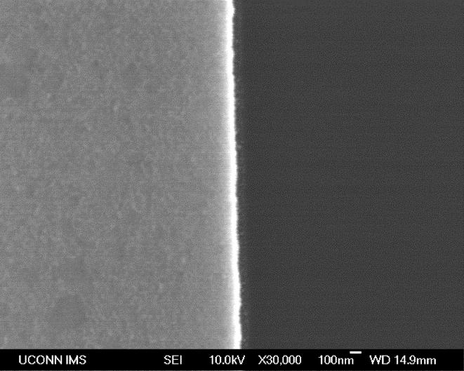
20 HIM Images Hang Dong, Rutgers < 9 nm < 7 nm HIM provides some estimates for gap size.


21 Nano-Nucleation Challenges Without UVO With UVO Growth is sensitive to surface pre-treatment, growth inhibition is observed without UVO. ALD metal films are not layer-by-layer, Nanograins form with inherent surface roughness. How smooth can we achieve? Could be shape dependence, crystal structure effects.
22 UV/Ozone Sample Pre-treatment XPS acetate-like planar films ALD Cu roughness values are similar to other reports 2, scales with thickness. UVO enhances/enables growth, removes most C 1s, but residual C remains even after long time (60 min). 2 Winter et al. Chem. Mater. v. 26, p (2014)


23 Selectivity High T growth, 230 C Annealed in He at 600 C prior to growth at 220 C Selectivity is lost at higher temperatures, inverted selectivity? Selectivity was a mystery; how does Cu grow on oxide?
24 ALD Fundamentals with in-situ SE note O content of precursor Cu(thd) 2 is a solid source precursor. H 2 is coreactant. In-situ, real time SE provides saturation curves.
25 SE Growth Trajectory ~15/466 = 0.03 delta/cycle in-situ SE provides growth finger-print, sensitive to substrate preparation and growth conditions. extracted GPC ~ 0.04 nm/cycle matches SEM data.
26 Original Mechanism Martensson s mechanism Cu(thd) 2 adsorbs to saturation during precursor dose. Martensson et al, JES, v. 145, p (1998)
27 SE Growth Signature Cu ALD SrO ALD SrO ALD shows characteristic signature for stable precursors adsorption. Cu ALD has opposite signature with reversible adsorption.
28 Original mechanism is NOT consistent with Cu I CVD by disproportionation at C, and can t explain observed GPC. Martensson et al, JES, v. 145, p (1998) Original Mechanism Martensson s mechanism Selectivity follows from H 2 dissociation requirement.

29 New Mechanism New mechanism explains SE signature and is consistent with reversible adsorption. Also explains high GPC. Roll of Pd-H 2 is now more complex, strong chemisorption.
30 SE Growth vs. Temperature Real-time SE vs. Temp Coverage Simulations CuL 2 + 2* CuL* + L* Mechanism not sensitive to temperature. H* must be stable. Dissociative reversible adsorption is consistent with thermodynamics if H ads ~ 34 kcal/mol.
 is consistent with RTSE data, GPC ~")
31 QCM Studies QCM measures mass and thermal effects. Reaction signal (at 150 C) is consistent with RTSE data, GPC ~ 0.04 nm/cycle.


32 Role of Pd XRD XPS Temperature and time dependence of Cu XRD and XPS signals indicate extensive Cu/Pd mixing. Lower temperatures = higher Cu/Pd ratios. ARXPS shows evidence for Pd enrichment at surface. Pd explains H chemisorption. What happens if the Pd runs out? Pd segregation


33 Cu/Pd vs. Cu/Pt Both Pt & Pd act as seed layers, but Pd mixes more extensively with Cu.

34 GPC on Pd/H* Cu ALD on Pd 150C GPC decreases as Cu/Pd becomes more Cu rich. Cu/Pd ratio measured as 45:1 for this sample.
35 Selectivity No adsorption/ desorption cycles for SiO 2, Si 3 N 4 Martensson et al, JES, v. 145, p (1998) Selectivity is evident from in-situ SE data, but how to explain non-selective growth on SiO 2?


36 Non-Selective Growth Mechanism? C 1s Growth on SiO 2 at 205 C O1s Cu 2p C 1s signal is removed by sputtering, but O 1s signal remains. Cu 2p signal could be Cu 0 or Cu I. Cu/O ratios are ~1.3. AES peaks indicates Cu I. CuO/Cu 2 O growth explains non-selective growth mechanism. Mechanism requires self-decomposition. H 2 not required, but may affect thickness. For thick Cu films, self-decomposition may contribute to growth.

 H 2 pressure plays a")
37 ph2 (Torr) H 2 effect on Non-selective Growth C 1.5 Torr Excellent Good Poor 160 C 3 Torr Temperature (C) H 2 pressure plays a significant role for non-selective growth. Why?

38 H 2 effect on Non-Selective Growth 180 C 180 C 1.5 torr H2 3 torr H C 0.5 torr H2
39 GPC(nm/cycle) H 2 Effect on Selective Growth Cu ALD on Pd Seed Layers C 160C H 2 partial pressure (torr) GPC Measured by QCM in selective window shows no effect of H 2 partial pressure. No growth without H 2.
40 Summary ALD Cu is useful for tuning the optical response of plasmonic materials. ALD of Ag, Au would be nice. Selective Area Cu ALD works well and is useful for tunnel junctions with many potential applications. Cu ALD mechanism is partially understood, Pd, H effects are important.
41 Acknowledgements Co-Pi s (Physics, Penn State): Darin Zimmerman, Gary Weisel, James Chen Students: X. Jiang & J. Qi (UCONN) R. Wamboldt (Penn State) Funding: NSF-EECS
The goal of this project is to enhance the power density and lowtemperature efficiency of solid oxide fuel cells (SOFC) manufactured by atomic layer
 manufactured by atomic layer") Stanford University Michael Shandalov1, Shriram Ramanathan2, Changhyun Ko2 and Paul McIntyre1 1Department of Materials Science and Engineering, Stanford University 2Division of Engineering and Applied
Stanford University Michael Shandalov1, Shriram Ramanathan2, Changhyun Ko2 and Paul McIntyre1 1Department of Materials Science and Engineering, Stanford University 2Division of Engineering and Applied
Shell-isolated nanoparticle-enhanced Raman spectroscopy
 Shell-isolated nanoparticle-enhanced Raman spectroscopy Jian Feng Li, Yi Fan Huang, Yong Ding, Zhi Lin Yang, Song Bo Li, Xiao Shun Zhou, Feng Ru Fan, Wei Zhang, Zhi You Zhou, De Yin Wu, Bin Ren, Zhong
Fabrication at the nanoscale for nanophotonics
 Fabrication at the nanoscale for nanophotonics Ilya Sychugov, KTH Materials Physics, Kista silicon nanocrystal by electron beam induced deposition lithography Outline of basic nanofabrication methods Devices
Nano Optics Based on Coupled Metal Nanoparticles
 Nano Optics Based on Coupled Metal Nanoparticles Shangjr Gwo ( 果尚志 ) Department of Physics National Tsing-Hua University, Hsinchu 30013, Taiwan E-mail: gwo@phys.nthu.edu.tw NDHU-Phys (2010/03/01) Background
Supplementary Figure 1 Experimental setup for crystal growth. Schematic drawing of the experimental setup for C 8 -BTBT crystal growth.
 Supplementary Figure 1 Experimental setup for crystal growth. Schematic drawing of the experimental setup for C 8 -BTBT crystal growth. Supplementary Figure 2 AFM study of the C 8 -BTBT crystal growth
Hydrogenation of Single Walled Carbon Nanotubes
 Hydrogenation of Single Walled Carbon Nanotubes Anders Nilsson Stanford Synchrotron Radiation Laboratory (SSRL) and Stockholm University Coworkers and Ackowledgement A. Nikitin 1), H. Ogasawara 1), D.
Modern Methods in Heterogeneous Catalysis Research: Preparation of Model Systems by Physical Methods
 Modern Methods in Heterogeneous Catalysis Research: Preparation of Model Systems by Physical Methods Methods for catalyst preparation Methods discussed in this lecture Physical vapour deposition - PLD
ALD-enabled nanopatterning: area-selective ALD by area-activation
 ALD-enabled nanopatterning: area-selective ALD by area-activation Adrie Mackus, Ageeth Bol, and Erwin Kessels w.m.m.kessels@tue.nl www.tue.nl/pmp Outline Introduction & Area-selective deposition Area-selective
Photovoltaic Enhancement Due to Surface-Plasmon Assisted Visible-Light. Absorption at the Inartificial Surface of Lead Zirconate-Titanate Film
 Photovoltaic Enhancement Due to Surface-Plasmon Assisted Visible-Light Absorption at the Inartificial Surface of Lead Zirconate-Titanate Film Fengang Zheng, a,b, * Peng Zhang, a Xiaofeng Wang, a Wen Huang,
B.-Y. Lin et al., Opt. Express 17, (2009).
.") !!!! The Ag nanoparticle array can be considered Ag nanorods arranged in hexagonal pattern with an inter-nanorod gap (W). The rod diameter (D) is 25 nm and the rod length (L) is 100 nm. A series of curved
!!!! The Ag nanoparticle array can be considered Ag nanorods arranged in hexagonal pattern with an inter-nanorod gap (W). The rod diameter (D) is 25 nm and the rod length (L) is 100 nm. A series of curved
Selective Manipulation of Molecules by Electrostatic Force and Detection of Single Molecules in Aqueous Solution
 Supporting Information Selective Manipulation of Molecules by Electrostatic Force and Detection of Single Molecules in Aqueous Solution Zhongbo Yan, Ming Xia, Pei Zhang, and Ya-Hong Xie* Department of
Simulated Study of Plasmonic Coupling in Noble Bimetallic Alloy Nanosphere Arrays
 CHAPTER 4 Simulated Study of Plasmonic Coupling in Noble Bimetallic Alloy Nanosphere Arrays 4.1 Introduction In Chapter 3, the noble bimetallic alloy nanosphere (BANS) of Ag 1-x Cu x at a particular composition
Supplementary material for High responsivity mid-infrared graphene detectors with antenna-enhanced photo-carrier generation and collection
 Supplementary material for High responsivity mid-infrared graphene detectors with antenna-enhanced photo-carrier generation and collection Yu Yao 1, Raji Shankar 1, Patrick Rauter 1, Yi Song 2, Jing Kong
Supplementary Figure S1. AFM images of GraNRs grown with standard growth process. Each of these pictures show GraNRs prepared independently,
 Supplementary Figure S1. AFM images of GraNRs grown with standard growth process. Each of these pictures show GraNRs prepared independently, suggesting that the results is reproducible. Supplementary Figure
Flexible, Transparent and Highly Sensitive SERS. Substrates with Cross-nanoporous Structures for
 Electronic Supplementary Material (ESI) for Nanoscale. This journal is The Royal Society of Chemistry 2018 supplementary information Flexible, Transparent and Highly Sensitive SERS Substrates with Cross-nanoporous
Understanding Nanoplasmonics. Greg Sun University of Massachusetts Boston
 Understanding Nanoplasmonics Greg Sun University of Massachusetts Boston Nanoplasmonics Space 100pm 1nm 10nm 100nm 1μm 10μm 100μm 1ns 100ps 10ps Photonics 1ps 100fs 10fs 1fs Time Surface Plasmons Surface
Planar Organic Photovoltaic Device. Saiful I. Khondaker
 Planar Organic Photovoltaic Device Saiful I. Khondaker Nanoscience Technology Center and Department of Physics University of Central Florida http://www.physics.ucf.edu/~khondaker W Metal 1 L ch Metal 2
A. Optimizing the growth conditions of large-scale graphene films
 1 A. Optimizing the growth conditions of large-scale graphene films Figure S1. Optical microscope images of graphene films transferred on 300 nm SiO 2 /Si substrates. a, Images of the graphene films grown
Supporting Information
 Supporting Information Yao et al. 10.1073/pnas.1416368111 Fig. S1. In situ LEEM imaging of graphene growth via chemical vapor deposition (CVD) on Pt(111). The growth of graphene on Pt(111) via a CVD process
Supplementary Figure 1: Power dependence of hot-electrons reduction of 4-NTP to 4-ATP. a) SERS spectra of the hot-electron reduction reaction using
 SERS spectra of the hot-electron reduction reaction using") Supplementary Figure 1: Power dependence of hot-electrons reduction of 4-NTP to 4-ATP. a) SERS spectra of the hot-electron reduction reaction using 633 nm laser excitation at different powers and b) the
Supplementary Figure 1: Power dependence of hot-electrons reduction of 4-NTP to 4-ATP. a) SERS spectra of the hot-electron reduction reaction using 633 nm laser excitation at different powers and b) the
Instrumentation and Operation
 Instrumentation and Operation 1 STM Instrumentation COMPONENTS sharp metal tip scanning system and control electronics feedback electronics (keeps tunneling current constant) image processing system data
Nova 600 NanoLab Dual beam Focused Ion Beam IITKanpur
 Nova 600 NanoLab Dual beam Focused Ion Beam system @ IITKanpur Dual Beam Nova 600 Nano Lab From FEI company (Dual Beam = SEM + FIB) SEM: The Electron Beam for SEM Field Emission Electron Gun Energy : 500
Electrochemically Synthesized Multi-block
 Electrochemically Synthesized Multi-block Nanorods Sungho Park SungKyunKwan University, Department of Chemistry & SKKU Advanced Institute of Nanotechnology (SAINT) J. Am. Chem. Soc. 2003, 125, 2282-2290
Fabrication Technology, Part I
 EEL5225: Principles of MEMS Transducers (Fall 2004) Fabrication Technology, Part I Agenda: Microfabrication Overview Basic semiconductor devices Materials Key processes Oxidation Thin-film Deposition Reading:
Wafer-scale fabrication of graphene
 Wafer-scale fabrication of graphene Sten Vollebregt, MSc Delft University of Technology, Delft Institute of Mircosystems and Nanotechnology Delft University of Technology Challenge the future Delft University
Spectroscopy at nanometer scale
 Spectroscopy at nanometer scale 1. Physics of the spectroscopies 2. Spectroscopies for the bulk materials 3. Experimental setups for the spectroscopies 4. Physics and Chemistry of nanomaterials Various
NTEGRA for EC PRESENTATION
 NTEGRA for EC PRESENTATION Application Purpose: In-situ control/modification of the surface morphology of single crystal and polycrystal electrodes (samples) during electrochemical process (in situ) in
A Plasmonic Photocatalyst Consisting of Silver Nanoparticles Embedded in Titanium Dioxide. Ryan Huschka LANP Seminar February 19, 2008
 A Plasmonic Photocatalyst Consisting of Silver Nanoparticles Embedded in Titanium Dioxide Ryan Huschka LANP Seminar February 19, 2008 TiO 2 Applications White Pigment Photocatalyst Previous methods to
Plasma Deposition (Overview) Lecture 1
 Lecture 1") Plasma Deposition (Overview) Lecture 1 Material Processes Plasma Processing Plasma-assisted Deposition Implantation Surface Modification Development of Plasma-based processing Microelectronics needs (fabrication
Plasma Deposition (Overview) Lecture 1 Material Processes Plasma Processing Plasma-assisted Deposition Implantation Surface Modification Development of Plasma-based processing Microelectronics needs (fabrication
High-density data storage: principle
 High-density data storage: principle Current approach High density 1 bit = many domains Information storage driven by domain wall shifts 1 bit = 1 magnetic nanoobject Single-domain needed Single easy axis
Supporting Information
 Supporting Information Superstructural Raman Nanosensors with Integrated Dual Functions for Ultrasensitive Detection and Tunable Release of Molecules Jing Liu #, Jianhe Guo #, Guowen Meng and Donglei Fan*
Supplementary information for
 Supplementary information for Transverse electric field dragging of DNA in a nanochannel Makusu Tsutsui, Yuhui He, Masayuki Furuhashi, Rahong Sakon, Masateru Taniguchi & Tomoji Kawai The Supplementary
Microscopical and Microanalytical Methods (NANO3)
") Microscopical and Microanalytical Methods (NANO3) 06.11.15 10:15-12:00 Introduction - SPM methods 13.11.15 10:15-12:00 STM 20.11.15 10:15-12:00 STS Erik Zupanič erik.zupanic@ijs.si stm.ijs.si 27.11.15
Microscopical and Microanalytical Methods (NANO3) 06.11.15 10:15-12:00 Introduction - SPM methods 13.11.15 10:15-12:00 STM 20.11.15 10:15-12:00 STS Erik Zupanič erik.zupanic@ijs.si stm.ijs.si 27.11.15
In situ Studies of ALD Processes & Reaction Mechanisms
 In situ Studies of ALD Processes & Reaction Mechanisms Erwin Kessels w.m.m.kessels@tue.nl www.tue.nl/pmp This tutorial presentation will give (1) an overview of methods for in situ studies of ALD processes
Energy transport in metal nanoparticle plasmon waveguides
 Energy transport in metal nanoparticle plasmon waveguides Stefan A. Maier, Pieter G. Kik, and Harry A. Atwater California Institute of Technology Thomas J. Watson Laboratory of Applied Physics, Pasadena,
Supporting Information
 Supporting Information Molecular Orbital Gating Surface-Enhanced Raman Scattering Chenyang Guo, 1, Xing Chen, 2, Song-Yuan Ding, 3, Dirk Mayer, 4 Qingling Wang, 1 Zhikai Zhao, 1,5 Lifa Ni, 1,6 Haitao Liu,
Nanomaterials for Plasmonic Devices. Lih J. Chen
 Nanomaterials for Plasmonic Devices Lih J. Chen Department of Materials Science and Engineering, National Tsing Hua University, Hsinchu, Taiwan Papers on Plasmon: 75,000 (6/25/2018) Papers on Plasmonics:
Size-dependent Metal-insulator Transition Random Materials Crystalline & Amorphous Purely Electronic Switching
 Nanometallic RRAM I-Wei Chen Department of Materials Science and Engineering University of Pennsylvania Philadelphia, PA 19104 Nature Nano, 6, 237 (2011) Adv Mater,, 23, 3847 (2011) Adv Func Mater,, 22,
2D Materials for Gas Sensing
 2D Materials for Gas Sensing S. Guo, A. Rani, and M.E. Zaghloul Department of Electrical and Computer Engineering The George Washington University, Washington DC 20052 Outline Background Structures of
Title of file for HTML: Supplementary Information Description: Supplementary Figures and Supplementary References
 Title of file for HTML: Supplementary Information Description: Supplementary Figures and Supplementary References Supplementary Figure 1. SEM images of perovskite single-crystal patterned thin film with
Supplementary Figure 1. Extinction spectra of rhodium nanocubes. UV-vis spectra of the Rh nanocubes in ethanol solution (black) and on a porous Al2O3
 and on a porous Al2O3") Supplementary Figure 1. Extinction spectra of rhodium nanocubes. UV-vis spectra of the Rh nanocubes in ethanol solution (black) and on a porous Al2O3 support (blue). The Rh nanocubes in ethanol solution
Supplementary Figure 1. Extinction spectra of rhodium nanocubes. UV-vis spectra of the Rh nanocubes in ethanol solution (black) and on a porous Al2O3 support (blue). The Rh nanocubes in ethanol solution
Secondaryionmassspectrometry
 Secondaryionmassspectrometry (SIMS) 1 Incident Ion Techniques for Surface Composition Analysis Mass spectrometric technique 1. Ionization -Electron ionization (EI) -Chemical ionization (CI) -Field ionization
NanoEngineering of Hybrid Carbon Nanotube Metal Composite Materials for Hydrogen Storage Anders Nilsson
 NanoEngineering of Hybrid Carbon Nanotube Metal Composite Materials for Hydrogen Storage Anders Nilsson Stanford Synchrotron Radiation Laboratory (SSRL) and Stockholm University Coworkers and Ackowledgement
Polarization control with plasmonic antenna-tips: A universal approach for optical nano-crystallography and vector-field imaging
 Supporting Information: Polarization control with plasmonic antenna-tips: A universal approach for optical nano-crystallography and vector-field imaging Kyoung-Duck Park 1,2 and Markus B. Raschke *1,2
In-situ Monitoring of Thin-Film Formation Processes by Spectroscopic Ellipsometry
 In-situ Monitoring of Thin-Film Formation Processes by Spectroscopic Ellipsometry Alexey Kovalgin Chair of Semiconductor Components MESA+ Institute for Nanotechnology Motivation Advantages of in-situ over
Plasma Chemistry Study in an Inductively Coupled Dielectric Etcher
 Plasma Chemistry Study in an Inductively Coupled Dielectric Etcher Chunshi Cui, John Trow, Ken Collins, Betty Tang, Luke Zhang, Steve Shannon, and Yan Ye Applied Materials, Inc. October 26, 2000 10/28/2008
Supporting Information
 Supporting Information Scalable Binder-Free Supersonic Cold Spraying of Nanotextured Cupric Oxide (CuO) Films as Efficient Photocathodes Jong Gun Lee, a,, Do-Yeon Kim, a,, Jong-Hyuk Lee, a, Min-woo Kim
Step Coverage by ALD Films: Theory and Examples
 Step Coverage by ALD Films: Theory and Examples of Ideal and Non-Ideal Reactions Roy G. Gordon Cambridge, MA 1 L Step Coverage in Holes with High Aspect Ratio Step coverage = (b/a) x 100% a Aspect ratio
Initial Stages of Growth of Organic Semiconductors on Graphene
 Initial Stages of Growth of Organic Semiconductors on Graphene Presented by: Manisha Chhikara Supervisor: Prof. Dr. Gvido Bratina University of Nova Gorica Outline Introduction to Graphene Fabrication
ALD Nucleation and Area-Selective Deposition
 ALD Nucleation and Area-Selective Deposition Prof Gregory N. Parsons Department of Chemical and Biomolecular Engineering North Carolina State University Raleigh North Carolina USA 1 Outline 1. Nucleation
Study of Surface Plasmon Excitation on Different Structures of Gold and Silver
 Nanoscience and Nanotechnology 2015, 5(4): 71-81 DOI: 10.5923/j.nn.20150504.01 Study of Surface Plasmon Excitation on Different Structures of Gold and Silver Anchu Ashok 1,*, Arya Arackal 1, George Jacob
TiO2/sapphire Beam Splitter for High-order Harmonics
 Technical Communication TiO2/sapphire Beam Splitter for High-order Harmonics Y. Sanjo*1, M. Murata*1, Y. Tanaka*1, H. Kumagai*1, and M. Chigane*2 *1 Graduate School of Engineering,Osaka City University,
Surface Chemistry and Reaction Dynamics of Electron Beam Induced Deposition Processes
 Surface Chemistry and Reaction Dynamics of Electron Beam Induced Deposition Processes e -? 2 nd FEBIP Workshop Thun, Switzerland 2008 Howard Fairbrother Johns Hopkins University Baltimore, MD, USA Outline
A Novel Electroless Method for the Deposition of Single-Crystalline Platinum Nanoparticle Films On
 Supplementary Information A Novel Electroless Method for the Deposition of Single-Crystalline Platinum Nanoparticle Films On an Organic Solid Matrix in the Presence of Gold Single Crystals Khaleda Banu,,,*
"Surface-Enhanced Raman Scattering
 SMR: 1643/11 WINTER COLLEGE ON OPTICS ON OPTICS AND PHOTONICS IN NANOSCIENCE AND NANOTECHNOLOGY ( 7-18 February 2005) "Surface-Enhanced Raman Scattering presented by: Martin Moskovits University of California,
Review of Nature Communications, NCOMMS In situ tracking of heterogeneous nanocatalytic processes. Reviewers' comments:
 Reviewers' comments: Reviewer #1 (Remarks to the Author): This manuscript describes measurement of surface enhanced Raman spectra (SERS) during CO oxidation catalysis on metal catalysts (E.g, Pt, FePt,
Theodore E. Madey. Department of Physics and Astronomy, and Laboratory for Surface Modification
 The Science of Catalysis at the Nanometer Scale Theodore E. Madey Department of Physics and Astronomy, and Laboratory for Surface Modification http://www.physics.rutgers.edu/lsm/ Rutgers, The State University
Supporting Information
 Supporting Information Direct Chemical Vapor Deposition-Derived Graphene Glasses Targeting Wide Ranged Applications Jingyu Sun, Yubin Chen, Manish Kr. Priydarshi, Zhang Chen, Alicja Bachmatiuk,, Zhiyu
Seminars in Nanosystems - I
 Seminars in Nanosystems - I Winter Semester 2011/2012 Dr. Emanuela Margapoti Emanuela.Margapoti@wsi.tum.de Dr. Gregor Koblmüller Gregor.Koblmueller@wsi.tum.de Seminar Room at ZNN 1 floor Topics of the
SEIRA effects. Annemarie Pucci
 SEIRA effects Annemarie Pucci Kirchhoff Institute of Physics, Heidelberg University 1. Introduction 2. SEIRA with metal-island films 3. SEIRA with metal dots 4. Dynamic charge transfer 5. Effect of nanoantenna
Large-Area and Uniform Surface-Enhanced Raman. Saturation
 Supporting Information Large-Area and Uniform Surface-Enhanced Raman Spectroscopy Substrate Optimized by Enhancement Saturation Daejong Yang 1, Hyunjun Cho 2, Sukmo Koo 1, Sagar R. Vaidyanathan 2, Kelly
Layer-modulated synthesis of uniform tungsten disulfide nanosheet using gas-phase precursors.
 Layer-modulated synthesis of uniform tungsten disulfide nanosheet using gas-phase precursors. Jusang Park * Hyungjun Kim School of Electrical and Electronics Engineering, Yonsei University, 262 Seongsanno,
Spring 2009 EE 710: Nanoscience and Engineering
 Spring 009 EE 710: Nanoscience and Engineering Part 10: Surface Plasmons in Metals Images and figures supplied from Hornyak, Dutta, Tibbals, and Rao, Introduction to Nanoscience, CRC Press Boca Raton,
Adjoint-Based Photonic Design: Optimization for Applications from Super-Scattering to Enhanced Light Extraction
 Adjoint-Based Photonic Design: Optimization for Applications from Super-Scattering to Enhanced Light Extraction Owen Miller Post-doc, MIT Applied Math PI: Steven Johnson Collaborators: Homer Reid (Math),
U-Shaped Nano-Apertures for Enhanced Optical Transmission and Resolution
 U-Shaped Nano-Apertures for Enhanced Optical Transmission and Resolution Mustafa Turkmen 1,2,3, Serap Aksu 3,4, A. Engin Çetin 2,3, Ahmet A. Yanik 2,3, Alp Artar 2,3, Hatice Altug 2,3,4, * 1 Electrical
(Co-PIs-Mark Brongersma, Yi Cui, Shanhui Fan) Stanford University. GCEP Research Symposium 2013 Stanford, CA October 9, 2013
 Stanford University. GCEP Research Symposium 2013 Stanford, CA October 9, 2013") High-efficiency thin film nano-structured multi-junction solar James S. cells Harris (PI) (Co-PIs-Mark Brongersma, Yi Cui, Shanhui Fan) Stanford University GCEP Research Symposium 2013 Stanford, CA October
High-efficiency thin film nano-structured multi-junction solar James S. cells Harris (PI) (Co-PIs-Mark Brongersma, Yi Cui, Shanhui Fan) Stanford University GCEP Research Symposium 2013 Stanford, CA October
Hotwire-assisted Atomic Layer Deposition of Pure Metals and Metal Nitrides
 Hotwire-assisted Atomic Layer Deposition of Pure Metals and Metal Nitrides Alexey Kovalgin MESA+ Institute for Nanotechnology Semiconductor Components group a.y.kovalgin@utwente.nl 1 Motivation 1. Materials
Supplementary Information
 Electronic Supplementary Material (ESI) for Nanoscale. This journal is The Royal Society of Chemistry 2014 Supplementary Information Large-scale lithography-free metasurface with spectrally tunable super
Cover Page. The handle holds various files of this Leiden University dissertation
 Cover Page The handle http://hdl.handle.net/1887/24306 holds various files of this Leiden University dissertation Author: Verhagen, T.G.A. Title: Magnetism and magnetization dynamics in thin film ferromagnets
J. Price, 1,2 Y. Q. An, 1 M. C. Downer 1 1 The university of Texas at Austin, Department of Physics, Austin, TX
 Understanding process-dependent oxygen vacancies in thin HfO 2 /SiO 2 stacked-films on Si (100) via competing electron-hole injection dynamic contributions to second harmonic generation. J. Price, 1,2
Plasma Etching: Atomic Scale Surface Fidelity and 2D Materials
 1 Plasma Etching: Atomic Scale Surface Fidelity and 2D Materials Thorsten Lill, Keren J. Kanarik, Samantha Tan, Meihua Shen, Alex Yoon, Eric Hudson, Yang Pan, Jeffrey Marks, Vahid Vahedi, Richard A. Gottscho
Shell-isolated nanoparticleenhanced Raman spectroscopy: Insight from COMSOL simulations
 Shell-isolated nanoparticleenhanced Raman spectroscopy: Insight from COMSOL simulations Song-Yuan Ding, Jun Yi, En-Ming You, and Zhong-Qun Tian 2016-11-03, Shanghai Excerpt from the Proceedings of the
Supporting Information for: Photo-induced force mapping of plasmonic. nanostructures
 Supporting Information for: Photo-induced force mapping of plasmonic nanostructures Thejaswi U. Tumkur,* # Xiao Yang,* # Benjamin Cerjan, Naomi J. Halas,*,,,, Peter Nordlander,*, Isabell Thomann*,,,, Corresponding
Supplementary Figures Supplementary Figure 1
 Supplementary Figures Supplementary Figure 1 Optical images of graphene grains on Cu after Cu oxidation treatment at 200 for 1m 30s. Each sample was synthesized with different H 2 annealing time for (a)
Lecture 11. Etching Techniques Reading: Chapter 11. ECE Dr. Alan Doolittle
 Lecture 11 Etching Techniques Reading: Chapter 11 Etching Techniques Characterized by: 1.) Etch rate (A/minute) 2.) Selectivity: S=etch rate material 1 / etch rate material 2 is said to have a selectivity
Characterisation of vibrational modes of adsorbed species
 17.7.5 Characterisation of vibrational modes of adsorbed species Infrared spectroscopy (IR) See Ch.10. Infrared vibrational spectra originate in transitions between discrete vibrational energy levels of
Surface Transfer Doping of Diamond by Organic Molecules
 Surface Transfer Doping of Diamond by Organic Molecules Qi Dongchen Department of Physics National University of Singapore Supervisor: Prof. Andrew T. S. Wee Dr. Gao Xingyu Scope of presentation Overview
Alternative deposition solution for cost reduction of TSV integration
 Alternative deposition solution for cost reduction of TSV integration J. Vitiello, F. Piallat, L. Bonnet KOBUS 611 rue Aristide Bergès, Z.A. de Pré Millet, Montbonnot-Saint-Martin, 38330 France Ph: +33
Film Deposition Part 1
 1 Film Deposition Part 1 Chapter 11 : Semiconductor Manufacturing Technology by M. Quirk & J. Serda Spring Semester 2013 Saroj Kumar Patra Semidonductor Manufacturing Technology, Norwegian University of
Energy fluxes in plasmas for fabrication of nanostructured materials
 Energy fluxes in plasmas for fabrication of nanostructured materials IEAP, Universität Kiel 2nd Graduate Summer Institute "Complex Plasmas" August 5-13, 2010 in Greifswald (Germany) AG 1 Outline Motivation
Photocatalysis: semiconductor physics
 Photocatalysis: semiconductor physics Carlos J. Tavares Center of Physics, University of Minho, Portugal ctavares@fisica.uminho.pt www.fisica.uminho.pt 1 Guimarães Where do I come from? 3 Guimarães 4 Introduction>>
Dry Plasma Reduction to Supported Platinum Nanoparticles for Flexible Dye-sensitized. Solar Cells. Yuseong-Gu, Daejeon , Korea
 Dry Plasma Reduction to Supported Platinum Nanoparticles for Flexible Dye-sensitized Solar Cells Van-Duong Dao a, Chinh Quoc Tran a, Seung-Hyeon Ko b, Ho-Suk Choi a * a Department of Chemical Engineering,
OPTICAL PROPERTIES AND SPECTROSCOPY OF NANOAAATERIALS. Jin Zhong Zhang. World Scientific TECHNISCHE INFORMATIONSBIBLIOTHEK
 OPTICAL PROPERTIES AND SPECTROSCOPY OF NANOAAATERIALS Jin Zhong Zhang University of California, Santa Cruz, USA TECHNISCHE INFORMATIONSBIBLIOTHEK Y World Scientific NEW JERSEY. t'on.don SINGAPORE «'BEIJING
The use of diagrams is good and the enhancement factors seen are reasonable but not in the league of gold or silver nanoparticles.
 Reviewers' comments: Reviewer #1 (Remarks to the Author): This is a very interesting article and should be published. The authors demonstrate a method to produce metallic MoO2 nano-dumbbells as SERS substrate
Surface plasmon waveguides
 Surface plasmon waveguides Introduction Size Mismatch between Scaled CMOS Electronics and Planar Photonics Photonic integrated system with subwavelength scale components CMOS transistor: Medium-sized molecule
A Novel Approach to the Layer Number-Controlled and Grain Size- Controlled Growth of High Quality Graphene for Nanoelectronics
 Supporting Information A Novel Approach to the Layer Number-Controlled and Grain Size- Controlled Growth of High Quality Graphene for Nanoelectronics Tej B. Limbu 1,2, Jean C. Hernández 3, Frank Mendoza
Special Properties of Au Nanoparticles
 Special Properties of Au Nanoparticles Maryam Ebrahimi Chem 7500/750 March 28 th, 2007 1 Outline Introduction The importance of unexpected electronic, geometric, and chemical properties of nanoparticles
From manipulation of the charge state to imaging of individual molecular orbitals and bond formation
 Scanning Probe Microscopy of Adsorbates on Insulating Films: From manipulation of the charge state to imaging of individual molecular orbitals and bond formation Gerhard Meyer, Jascha Repp, Peter Liljeroth
Supplementary Figure 1 Detailed illustration on the fabrication process of templatestripped
 Supplementary Figure 1 Detailed illustration on the fabrication process of templatestripped gold substrate. (a) Spin coating of hydrogen silsesquioxane (HSQ) resist onto the silicon substrate with a thickness
There's Plenty of Room at the Bottom
 There's Plenty of Room at the Bottom 12/29/1959 Feynman asked why not put the entire Encyclopedia Britannica (24 volumes) on a pin head (requires atomic scale recording). He proposed to use electron microscope
A Photonic Crystal Laser from Solution Based. Organo-Lead Iodide Perovskite Thin Films
 SUPPORTING INFORMATION A Photonic Crystal Laser from Solution Based Organo-Lead Iodide Perovskite Thin Films Songtao Chen 1, Kwangdong Roh 2, Joonhee Lee 1, Wee Kiang Chong 3,4, Yao Lu 5, Nripan Mathews
Surface Plasmon Resonance in Metallic Nanoparticles and Nanostructures
 Surface Plasmon Resonance in Metallic Nanoparticles and Nanostructures Zhi-Yuan Li Optical Physics Laboratory, Institute of Physics, CAS Beijing 18, China January 5-9, 7, Fudan University, Shanghai Challenges
Supplementary Information. Characterization of nanoscale temperature fields during electromigration of nanowires
 Supplementary Information Characterization of nanoscale temperature fields during electromigration of nanowires Wonho Jeong,, Kyeongtae Kim,, *, Youngsang Kim,, Woochul Lee,, *, Pramod Reddy Department
High-resolution Characterization of Organic Ultrathin Films Using Atomic Force Microscopy
 High-resolution Characterization of Organic Ultrathin Films Using Atomic Force Microscopy Jing-jiang Yu Nanotechnology Measurements Division Agilent Technologies, Inc. Atomic Force Microscopy High-Resolution
SUPPLEMENTARY INFORMATION
 doi:.38/nature09979 I. Graphene material growth and transistor fabrication Top-gated graphene RF transistors were fabricated based on chemical vapor deposition (CVD) grown graphene on copper (Cu). Cu foil
Supplementary Figure 1 Scheme image of GIXD set-up. The scheme image of slot die
 Supplementary Figure 1 Scheme image of GIXD set-up. The scheme image of slot die printing system combined with grazing incidence X-ray diffraction (GIXD) set-up. 1 Supplementary Figure 2 2D GIXD images
Supporting Information
 Supporting Information Under-Oil Switchable Superhydrophobicity to Superhydrophilicity Transition on TiO 2 Nanotube Arrays Hongjun Kang, Yuyan Liu, Hua Lai, Xiaoyan Yu, Zhongjun Cheng, and Lei Jiang MIIT
Supplementary Information. Atomic Layer Deposition of Platinum Catalysts on Nanowire Surfaces for Photoelectrochemical Water Reduction
 Supplementary Information Atomic Layer Deposition of Platinum Catalysts on Nanowire Surfaces for Photoelectrochemical Water Reduction Neil P. Dasgupta 1 ǂ, Chong Liu 1,2 ǂ, Sean Andrews 1,2, Fritz B. Prinz
Transparent Electrode Applications
 Transparent Electrode Applications LCD Solar Cells Touch Screen Indium Tin Oxide (ITO) Zinc Oxide (ZnO) - High conductivity - High transparency - Resistant to environmental effects - Rare material (Indium)
SUPPLEMENTARY INFORMATION
 Supplementary Information: Photocurrent generation in semiconducting and metallic carbon nanotubes Maria Barkelid 1*, Val Zwiller 1 1 Kavli Institute of Nanoscience, Delft University of Technology, Delft,