Procédés de dépôt plasma avec injection pulsée de précurseurs (PECVD et PEALD) :
|
|
|
- Ruby Jennings
- 5 years ago
- Views:
Transcription
 : Impact du réacteur et de la pression et")


1 Procédés de dépôt plasma avec injection pulsée de précurseurs (PECVD et PEALD) : Impact du réacteur et de la pression et développement de dépôts sélectifs C. Vallée 1,3, R. Gassilloud 2, R. Vallat 1,2, V. Pesce 1,2, S. Belahcen 1, A. Chaker 1, O. Salicio 1, N. Posseme 2, P. Gonon 1, M. Bonvalot 1, and A. Bsiesy 1 1 Univ. Grenoble Alpes, Lab. LTM (CEA-LETI/MINATEC) - Grenoble France 2 CEA-LETI / MINATEC Grenoble France 3 University of Tsukuba, Faculty of Pure and Applied Physics Tsukuba Japan
 - HDP-CVD process for gap filling is using a low pressure plasma discharge with inductive source PECVD TEOS HDP CVD silane D.R.")
2 PECVD parameters PECVD in microelectronics - Mainly capacitive discharges working at high pressure (> Torr) - Plasma damage, no need for ions - High throughput manufacturing - Uniformity (2% from center to edge) - HDP-CVD process for gap filling is using a low pressure plasma discharge with inductive source PECVD TEOS HDP CVD silane D.R. Cote et al, IBM Journal of Research and Development, Plasma processing, 43 (1/2), 1999

3 PECVD parameters PECVC process with CCP RF reactor Parameters to turn for the process: - Plasma Power: plasma density, flux, energy - Pressure: reactions in the plasma, T e, sheath collisionless or not - residence time: plasma/surface interactions
4 PECVD parameters Can we find more parameters to turn? RF generator frequency Pulsing the plasma or the precursors What can be pulsed? All parameters can be pulsed: Plasma modulation: modification of discharge chemistry, decrease the ion to neutral flux ratio on the substrate, presence of long life time active species which act as precursors to the film growth, decrease substrate temperature Precursors: control of thickness, plasma chemistry, conformality composition, stress and properties of thin film
5 From PECVD to PEALD PECVD Reactive plasma gas ON OFF Precursor ON OFF
6 From PECVD to PEALD Reactive plasma gas ON OFF Reactive plasma gas PECVD ON OFF AVD / PECVD with DLI Pulsing the precursor OFF ON Pulsing the plasma ON Precursor ON OFF OFF Pulsed PECVD Precursor ON OFF
7 From PECVD to PEALD PECVD Reactive plasma gas ON OFF AVD / PECVD with DLI Pulsing the precursor ON Reactive Plasma gas Purge PEALD ON 3 OFF ON 2 OFF 4 Reactive plasma gas ON OFF OFF ON 1 OFF Precursor Precursor ON OFF Pulsing the plasma ON OFF Pulsed PECVD Reactive gas Plasma ON 2 OFF ON Precursor ON OFF ON 1 OFF Precursor

8 ALD Atomic layer deposition (ALD) is a CVD technique that can achieve unparalleled control at the atomic scale. ALD achieves bottom-up control through chemical reactions with special characteristics: reactions take place at the surface only gas-phase reactions are inhibited; reactions are self-limiting but can be re-activated; reactions take place independent of fluctuations in external conditions the same chemistry thus applies at all scales Cyclic deposition (no reactions between the precursor and the reactant)
 is forecasted to be the fastest growing segment, with a compound annual growth rate of 19.9 percent, the market research firm estimates.")
9 Solid State Technology and Global Industry Analysts (GIA): the global deposition equipment market will hit $13.6 billion by Atomic layer deposition (ALD) is forecasted to be the fastest growing segment, with a compound annual growth rate of 19.9 percent, the market research firm estimates. 8 billions USD The 3D device inflection is driving growth in ALD with demands for new patterning films, new conformal materials and lower thermal budgets
10 PEALD 1) 2) Surface Initiale From Oxford instrument Profijt et al., J. Vac. Sci. Technol. A 29 (5) (2011) Comparison between thermal ALD and PE-ALD Al 2 O 3 - Al(CH 3 ) 3 and H 2 O Al(CH 3 ) 3 exposure 3) Purge 4) H 2 O exposure 5) Purge
 050801 (2011) Comparison between thermal ALD and PE-ALD Al 2 O 3 - Al(CH 3 ) 3 and O 2 plasma Al(CH 3 ) 3 exposure O 2 plasma 3)")
11 1) 2) Surface Initiale PEALD From Oxford instrument Profijt et al., J. Vac. Sci. Technol. A 29 (5) (2011) Comparison between thermal ALD and PE-ALD Al 2 O 3 - Al(CH 3 ) 3 and O 2 plasma Al(CH 3 ) 3 exposure O 2 plasma 3) Purge 4) H 2 Oexposure 2 plasma 5) Purge exposure
12 Cold plasmas for ALD Only used for the activation step. If used during the injection of precursor: PECVD process without self-limited reaction Cold plasmas reservoir of radicals for oxidation (O from O 2 reduction (H from H 2 or NH 3 plasma) steps plasma), or General idea: ions flowing to the surface are too energetic particles for ALD with creation of defects, roughness and not self-limiting step they must be removed specific design of plasma reactors for PEALD capacitive discharge with grids to remove ions high density plasma sources (inductive, microwave) used as a remote discharge: distance between plasma source and substrate is higher than the mean free path of ions ; all ions are loosed when travelling from their creation to the substrate
 No ion bombardment (grid) Substrate where the plasma is ignited Ion bombardment (direct plasma) Plasma damage Substrate heating No control of ion")
13 PEALD plasma reactors All reactor have advantages and defaults ASM / BENEQ / TEL Plasma uniformity / substrate High flux of radicals (/ions) Double frequency High Pressure (collisional sheath) No ion bombardment (grid) Substrate where the plasma is ignited Ion bombardment (direct plasma) Plasma damage Substrate heating No control of ion energy


14 PEALD plasma reactors All reactor have advantages and defaults PICOSUN / OXFORD Remote plasma Substrate not in the plasma ignition zone Control of ion energy may be possible Plasma uniformity Plasma damage Limited to low/moderate pressure
 ammonia (NH 3 ) at 500 C in a furnace A batch")

15 Batch tool Si 3 N 4 ALD process with dichlorosilane (DCS) and ionized (plasma) ammonia (NH 3 ) at 500 C in a furnace A batch furnace can process up to 100 wafers at the same time, which makes the process more cost effective compared to single wafer process. (5nm ~1 hour)
16 PEALD Plasma ALD is (may) using same precursors than thermal ALD Only the gas nature of the activation step is modified Material ALD precursor Plasma gas Oxide H 2 O ou O 3 O 2 Nitride NH 3 N 2 /H 2 Metal O 2, N 2 /H 2, H 2 from Oxford Instrument
17 Thermal ALD vs PEALD: Al 2 O 3 Long purge times with H 2 O at low temperature Decrease is attributed to thermally activated recombination reactions of surface hydroxyl groups OH (dehydroxylation) Source: Oxford instruments


18 PEALD For Area Selective Deposition - What is ASD? - ASD for microelectronics? - A way to do it: add a plasma etching step in PEALD step
19 What is Area Selective Deposition? Hey guys I need a thin oxide deposition on my two wafers
: let s go! D.R.")
20 What is Area Selective Deposition? Hey guys I need a thin oxide deposition on my two wafers PVD man (70/80 s): let s go! D.R. Cote et al, IBM Journal of Research and Development, Plasma processing, 43 (1/2), 1999
21 What is Area Selective Deposition? Hey guys I need a thin oxide deposition on my two wafers (PE)CVD man (80/90 s): In can do better for the 3D substrate! D.R. Cote et al, IBM Journal of Research and Development, Plasma processing, 43 (1/2), 1999
ALD man (2000 s): No ways, I am the best!")
22 What is Area Selective Deposition? Hey guys I need a thin oxide deposition on my two wafers (PE)ALD man (2000 s): No ways, I am the best! «ALD break materials, conformality barriers», A.E. Braun, Semiconductor Int. Octobre 2001

23 What is Area Selective Deposition? Hey guys I need a thin oxide deposition on my two wafers ASD man (now to..): I can select the area! A. Chaker et al, to be published

 How can we obtain")
?")
24 PVD, (PE)CVD, ALD: Deposition of thin films is made in the z direction (control of the thickness) How can we obtain the control of the two other directions (x,y)? Patterning top down approach


25 Patterning steps TOP DOWN approach Lithography step: resist deposition + mask definition Stripping: mask etching Plasma etching step: mask transfer


")


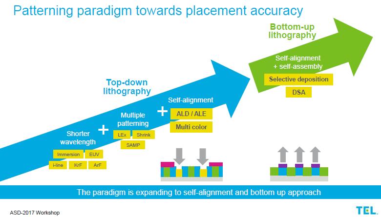
26 More an more complex patterning using two of several steps of patterning (masks and exposure) alignment for is crucial G.N. Parsons ALD2018 tutorial

27 Resolution needed for the scaling of the pitch is no more following the wavelength of the stepper introduction of complex multiple patterning processes
 Conformal deposition High")
28 Self-Aligned Quadruple Patterning: the pitch is reduced by a factor of 4 Material used for spacer» SiO 2 and Si 3 N 4 by PEALD Low T ( C) Conformal deposition High quality
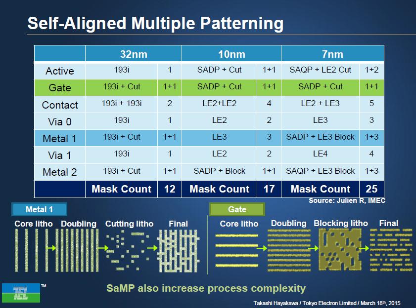
29 Multipatterning processes is needed for actual and future transistors Increase of wafer cost Misalignment errors Patterning method Normalized cost per wafer Single Exposure (SE) 1 Litho Etch Litho Etch (LELE) 2.5 Litho Etch Litho Etch Litho Etch (LELELE) 3.5 Self-Aligned Double Patterning (SADP) 2 Self-Aligned Quadruple Patterning (SAQP) 3 Extreme UV (EUV) Single Exposure (SE) 4 EUV + SADP 6 A. Raley et al., Proc. SPIE 9782, 97820F (2016)
30
31


32 Area Selective Deposition: new bottom-up approach growth is controlled in the 3 directions The deposition can depend on the chemical nature of the surface (no deposition on metallic surface)


33 The deposition can also be selective in one direction versus the others More complex: surface selectivity + directional growth


34 Why using ALD for ASD? ALD Cyclic deposition Self-limiting reactions Very conformal Very sensitive to the surface In this ALD example, deposition starts from a OH terminated surface
35 Precursors may react with one substrate, but not with another A precursor may etch away a substrate or react with subsurface layers. Or a precursor may not react at all on a substrate - such nucleation delays are common, e.g. for oxides on H-terminated silicon or for metals on oxides The ADL growth can start from the first cycle but delays may also be observed M. A. Alam, and M. L. Green Journal of Applied Physics, (2003) Film thickness (Å) Substrate effects Number of ALD cycles

36 This can be used for ASD, it is ASD by inherent selectivity - It can be inherent or induced by a post deposition treatment - Need better understanding between surface and precursors interactions BUT: Most of the time the selective thickness is limited to few nm Tungsten nucleation delay is substrate dependent - Surface bound water inhibits W-ALD nucleation - SiH 4 pre-exposure promote nucleation J. W. Elam ECS Transactions, (2007)


37 Two strategies to improve the selectivity: - using an area activation, - using an area deactivation

38 BUT: whatever the choice, a deposition may occur where it is not wanted after a given number of cycles (SAM not dense enough, SAM are reduces/modifies by a plasma,.) Need to introduce corrective action: etching of undesired material


39 Etching will enable a perfect ASD? 1. Different nucleation time between two surfaces A and B is needed (inherent selectivity, surface treatment ) 2. Precise etching at the nanometer scale to remove the deposited material from surface B 3. Add a new nucleation delay time for the surface B after or during the etching step A B A
 01B104 (2017) Need to do both Deposition (PEALD) and Etching (ALE ) in the")
40 R. Vallat, R. Gassilloud, B. Eychenne, and C. Vallée, J. Vac. Sci Technol. A 35(1) 01B104 (2017) Need to do both Deposition (PEALD) and Etching (ALE ) in the same tool
41 GO BACK TO SLIDE 13: HOW CAN WE DO THAT WITH THIS APPROACH?
42 Selective Deposition anisotropic etching ion sputt., RIE, anisotropic ALE anisotropic etching ion sputt., RIE, anisotropic ALE isotropic etching chem. etching, isotropic ALE
43 PEALD (8 cycles) Etching cycle PEALD (8 cycles) Precursor O 2 Plasma Power Etching gas When? Every cycle, every 5 cycles, throughput of the process How long? 1s? 3s?... throughput of the process, not perfect ASD (undesired material not removed / all the desired material is removed) Why does it work and how improve it? Plasma and precursor /surface reactions, contamination
44 Ta 2 O 5 ASD: PEALD Ta 2 O 5 + Ar plasma PEALD deposition step Plasma potential V p Non-collisional sheath 0 V MB P rf 0 W
45 Ta 2 O 5 ASD: PEALD Ta 2 O 5 + Ar plasma PEALD deposition step Plasma potential V p Ar plasma sputt. step Plasma potential V p Non-collisional sheath Non-collisional sheath 0 V V dc (self-bias) + MB MB P rf 0 W P rf
46 Ta 2 O 5 ASD: PEALD Ta 2 O 5 + Ar plasma Need a good control of ion energy Low pressure plasma (non-collisional sheath) HDP source (inductive ) Ion energy = e(v p -V dc ) Ar plasma sputt. step MB Plasma potential V p Non-collisional sheath V dc (self-bias) + P rf
 with substrate biasing platform and in situ ellipsometry")
47 Ta 2 O 5 ASD: PEALD Ta 2 O 5 + Ar plasma PEALD tool from Oxford (FLEXAL) with substrate biasing platform and in situ ellipsometry (film sense)

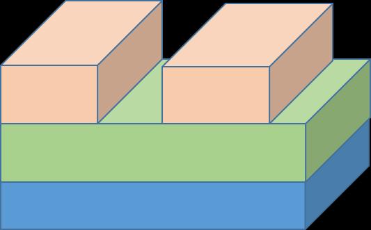
48 Case 1: Trenches - Aspect Ratio = A. Chaker et al, to be published

49 A. Chaker et al, to be published 2 Ta 2 O 5 conformal deposition No deposition

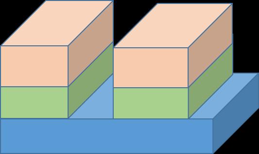
50 4 Ta 2 O 5 conformal deposition No deposition A. Chaker et al, to be published

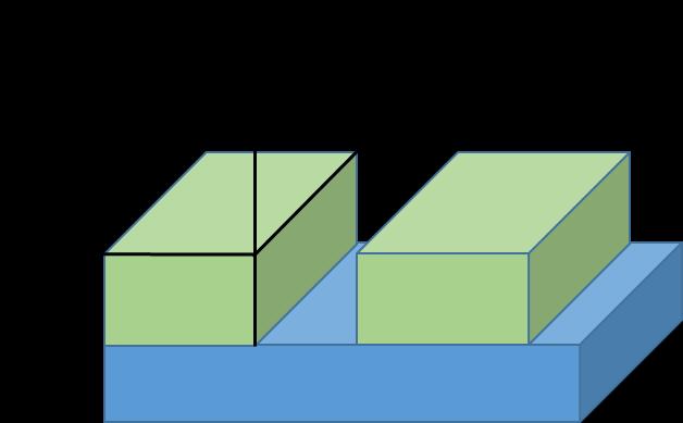
51 3 1 2 Case 2: Cylinder structure - Aspect Ratio = 5 A. Chaker et al, to be published

52 Conformal Ta 2 O 5 deposition Conformal Ta 2 O 5 deposition No deposition 2 A. Chaker et al, to be published

53 No deposition Conformal Ta 2 O 5 deposition 3 A. Chaker et al, to be published

54 Example 2 of ASD using etching OK this is done but can we dome something more complicated directional selective deposition + surface selective deposition using ion sputtering is no more a good solution

 with in situ XPS 300 mm CCP PEALD")
55 Example 2 of ASD using etching Need of a chemical ISOTROPIC etching Etching must be done by radicals only Can be done in CCP discharge at high pressure (collisional sheath) Process developed in 300 mm tool from KOBUS (capacitive discharge) with in situ XPS 300 mm CCP PEALD tool
56 Plasma is used to create delays in nucleation PEALD of TiO 2 before and after NF 3 plasma (Kobus tool) Thickness (nm) Without NF treatment 3 With NF treatment 3 No effect on TiN substrate b) TiN substrate Thickness (nm) Without NF treatment 3 With NF treatment 3 Additional nucleation time a) for Si substrate Si substrate Number of cycles Number of cycles R. Vallat, et al J. Vac. Sci Technol. A 35(1) 01B104 (2017)
57 Impact of Fluorine-based plasma? (Example with ASD of TiO 2 ) Quasi in situ XPS to understand and optimize the passivation step From quasi in situ XPS we can estimate the nucleation delay induced by Fluorinebased plasma to be 5-10 PEALD cycles O. Salicio et al, to be published
58 Plasma is also used to etch material Etching of TiO 2 n NF 3 /O 2 /Ar plasma Etching thickness (A) Etching time (s) The etching step must be made at the same temperature than the deposition temperature F-based plasma good candidate: TiF 4 volatile at 250 C
59 Growth starts faster on TiN substrate (inherent or plasma treatment) TiN Si TiN After X cycles TiO 2 starts to growth on both substrates TiN Si TiN
60 NF 3 is added to O 2 plasma to etch TiO 2 and create Si-F bonds (few Ti-F bonds) F F F F F F F F F F F F F F F F F F F F TiN Si TiN After a number of PEALD cycles TiO 2 starts to growth on both substrates due to F removal on Si substrate by O 2 plasma: NF 3 again to etch and create new Si-F bonds TiN Si TiN
61 NF 3 is added to O 2 plasma to etch TiO 2 and create Si-F bonds (few Ti-F bonds) F F F F F F F F F F F F F F F F F F F F TiN Si TiN After a number of PEALD cycles TiO 2 starts to growth on both substrates due to F removal on Si substrate by O 2 plasma: NF 3 again to etch and create new Si-F bonds F F F F F F F F F F F F F F F F F F F F TiN Si TiN
62 Need to optimize the PEALD / etching cycles ratio! F F F F F F F F F F F F F F F F TiN Si TiN
 + plasma etching (1 cycle) = 1 super cycle Selective")
 with TBTDET (TDEAT) and O")
tris(diethylamido)tantalum")
63 Selective deposition of TiO 2 and Ta 2 O 5 on TiN versus Si substrate PEALD (x cycles) + plasma etching (1 cycle) = 1 super cycle Selective deposition = x super cycles Presentation today: selective deposition of Ta 2 O 5 and TiO 2 PEALD of Ta 2 O 5 (TiO 2 ) with TBTDET (TDEAT) and O 2 plasma Tetrakis(diethylamido)titanium (TDEATi) Etching cycle by adding fluorine-based plasma tert-butylimido)tris(diethylamido)tantalum (TBTDET)
64 All requirements are ok! Let s go for selective deposition In the selective deposition process for Ta 2 O 5 we only slightly modified the PEALD process by adding a NF 3 pulse in O 2 pulse every 8 cycles* (O 2 /Ar (250 / 2500 scm - 75W plasma 2 Torr) PEALD (8 cycles) Etching cycle PEALD (8 cycles) TBTDET precursor O 2 Plasma Power NF 3 For TiO 2 the number of PEALD cycles before plasma etching exposure has been fixed to 20 *More details in: R. Vallat, R. Gassilloud, B. Eychenne, and C. Vallée J. Vac. Sci Technol. A 35(1) 01B104 (2017)
65 Ta 2 O 5 Si SiO 2 TiN Number of Ta 2 O 5 thickness Ta 2 O 5 thickness Ta 2 O 5 density super cycles on Si / SiO 2 (nm) on TiN (nm) (g.cm -3 ) 11 0 / / R. Vallat, R. Gassilloud, B. Eychenne, and C. Vallée J. Vac. Sci Technol. A 35(1) 01B104 (2017)
66 Number of super cycles Ta 2 O 5 thickness on Si / SiO 2 (nm) Ta 2 O 5 thickness on TiN (nm) Ta 2 O 5 density (g.cm -3 ) 11 0 / / Number of super cycles TiO 2 thickness on Si (nm) TiO 2 thickness on TiN (nm) TiO 2 density (g.cm -3 ) Density is slightly reduced when increasing the number of super cycles: Origin? Voids? Contamination by F atoms? Impact on electrical properties?
 TiN TiN SiO 2 Si 3 N 4 Si R. Vallat et al.")
67 ASD on 3D patterned substrate (SEM image by M. Fraccaroli) TiN TiN SiO 2 Si 3 N 4 Si R. Vallat et al. submitted to JVSTA
 R. Vallat et al.")
68 ASD on 3D patterned substrate (SEM image by M. Fraccaroli) R. Vallat et al. submitted to JVSTA TiN TiN SiO 2 Si 3 N 4 Si


69 TiN TiN SiO 2 Si 3 N 4 Si R. Vallat et al. submitted to JVSTA


70 a. b. R. Vallat et al. submitted to JVSTA
71 Conclusion - Not radicals only can be useful for PEALD processes - Depending on the materials, ions can increase/decrease the GPC, modify the density, roughness, crystalline phase. Ions can also be used for area selective deposition on 3D patterned substrates - What about the others? UV photons, O 3. - Whatever the ASD process (SAM,,...), etching is needed to improve selectivity - Optimum goal: ALD + ALE ALE in the PEALD FLEXAL tool is now optimized Thickness variation (nm) CF 4 + purge ALE of Ta 2 O 5 O 2 /CF 4 plasma + Ar plasma 5W bias (-45 V) Ar plasma CF 4 + purge Ar plasma CF 4 + purge Ar plasma CF 4 + purge Ar plasma Time (s)

72 Futur trends: All is Atomic Layer Processing
Chapter 7 Plasma Basic
 Chapter 7 Plasma Basic Hong Xiao, Ph. D. hxiao89@hotmail.com www2.austin.cc.tx.us/hongxiao/book.htm Hong Xiao, Ph. D. www2.austin.cc.tx.us/hongxiao/book.htm 1 Objectives List at least three IC processes
Plasma Deposition (Overview) Lecture 1
 Lecture 1") Plasma Deposition (Overview) Lecture 1 Material Processes Plasma Processing Plasma-assisted Deposition Implantation Surface Modification Development of Plasma-based processing Microelectronics needs (fabrication
Plasma Deposition (Overview) Lecture 1 Material Processes Plasma Processing Plasma-assisted Deposition Implantation Surface Modification Development of Plasma-based processing Microelectronics needs (fabrication
Patterning Challenges and Opportunities: Etch and Film
 Patterning Challenges and Opportunities: Etch and Film Ying Zhang, Shahid Rauf, Ajay Ahatnagar, David Chu, Amulya Athayde, and Terry Y. Lee Applied Materials, Inc. SEMICON, Taiwan 2016 Sept. 07-09, 2016,
Chapter 7. Plasma Basics
 Chapter 7 Plasma Basics 2006/4/12 1 Objectives List at least three IC processes using plasma Name three important collisions in plasma Describe mean free path Explain how plasma enhance etch and CVD processes
Etching: Basic Terminology
 Lecture 7 Etching Etching: Basic Terminology Introduction : Etching of thin films and sometimes the silicon substrate are very common process steps. Usually selectivity, and directionality are the first
Selective Processes: Challenges and Opportunities in Semiconductor Scaling
 Selective Processes: Challenges and Opportunities in Semiconductor Scaling June 4, 2018 Kandabara Tapily TEL Technology Center, America, LLC IITC 2018 Selective Deposition Workshop K. Tapily/ IITC 2018
ETCHING Chapter 10. Mask. Photoresist
 ETCHING Chapter 10 Mask Light Deposited Substrate Photoresist Etch mask deposition Photoresist application Exposure Development Etching Resist removal Etching of thin films and sometimes the silicon substrate
Etching Issues - Anisotropy. Dry Etching. Dry Etching Overview. Etching Issues - Selectivity
 Etching Issues - Anisotropy Dry Etching Dr. Bruce K. Gale Fundamentals of Micromachining BIOEN 6421 EL EN 5221 and 6221 ME EN 5960 and 6960 Isotropic etchants etch at the same rate in every direction mask
CVD: General considerations.
 CVD: General considerations. PVD: Move material from bulk to thin film form. Limited primarily to metals or simple materials. Limited by thermal stability/vapor pressure considerations. Typically requires
FRAUNHOFER IISB STRUCTURE SIMULATION
 FRAUNHOFER IISB STRUCTURE SIMULATION Eberhard Bär eberhard.baer@iisb.fraunhofer.de Page 1 FRAUNHOFER IISB STRUCTURE SIMULATION Overview SiO 2 etching in a C 2 F 6 plasma Ga ion beam sputter etching Ionized
Hotwire-assisted Atomic Layer Deposition of Pure Metals and Metal Nitrides
 Hotwire-assisted Atomic Layer Deposition of Pure Metals and Metal Nitrides Alexey Kovalgin MESA+ Institute for Nanotechnology Semiconductor Components group a.y.kovalgin@utwente.nl 1 Motivation 1. Materials
Section 3: Etching. Jaeger Chapter 2 Reader
 Section 3: Etching Jaeger Chapter 2 Reader Etch rate Etch Process - Figures of Merit Etch rate uniformity Selectivity Anisotropy d m Bias and anisotropy etching mask h f substrate d f d m substrate d f
Reactive Ion Etching (RIE)
") Reactive Ion Etching (RIE) RF 13.56 ~ MHz plasma Parallel-Plate Reactor wafers Sputtering Plasma generates (1) Ions (2) Activated neutrals Enhance chemical reaction 1 2 Remote Plasma Reactors Plasma Sources
Reactive Ion Etching (RIE) RF 13.56 ~ MHz plasma Parallel-Plate Reactor wafers Sputtering Plasma generates (1) Ions (2) Activated neutrals Enhance chemical reaction 1 2 Remote Plasma Reactors Plasma Sources
EE143 Fall 2016 Microfabrication Technologies. Lecture 6: Thin Film Deposition Reading: Jaeger Chapter 6
 EE143 Fall 2016 Microfabrication Technologies Lecture 6: Thin Film Deposition Reading: Jaeger Chapter 6 Prof. Ming C. Wu wu@eecs.berkeley.edu 511 Sutardja Dai Hall (SDH) 1 Vacuum Basics Units 1 atmosphere
Lecture 6 Plasmas. Chapters 10 &16 Wolf and Tauber. ECE611 / CHE611 Electronic Materials Processing Fall John Labram 1/68
 Lecture 6 Plasmas Chapters 10 &16 Wolf and Tauber 1/68 Announcements Homework: Homework will be returned to you on Thursday (12 th October). Solutions will be also posted online on Thursday (12 th October)
Device Fabrication: Etch
 Device Fabrication: Etch 1 Objectives Upon finishing this course, you should able to: Familiar with etch terminology Compare wet and dry etch processes processing and list the main dry etch etchants Become
4FNJDPOEVDUPS 'BCSJDBUJPO &UDI
 2010.5.4 1 Major Fabrication Steps in CMOS Process Flow UV light oxygen Silicon dioxide Silicon substrate Oxidation (Field oxide) photoresist Photoresist Coating Mask exposed photoresist Mask-Wafer Exposed
Atomic layer deposition of titanium nitride
 Atomic layer deposition of titanium nitride Jue Yue,version4, 04/26/2015 Introduction Titanium nitride is a hard and metallic material which has found many applications, e.g.as a wear resistant coating[1],
ALD & ALE Tutorial Speakers and Schedule
 ALD & ALE Tutorial Speakers and Schedule Sunday, July 29, 2018 1:00-1:05 Tutorial Welcome 1:05-1:50 1:50-2:35 2:35-3:20 Challenges of ALD Applications in Memory Semiconductor Devices, Choon Hwan Kim (SK
ALD Nucleation and Area-Selective Deposition
 ALD Nucleation and Area-Selective Deposition Prof Gregory N. Parsons Department of Chemical and Biomolecular Engineering North Carolina State University Raleigh North Carolina USA 1 Outline 1. Nucleation
Fabrication Technology, Part I
 EEL5225: Principles of MEMS Transducers (Fall 2004) Fabrication Technology, Part I Agenda: Microfabrication Overview Basic semiconductor devices Materials Key processes Oxidation Thin-film Deposition Reading:
EE-612: Lecture 22: CMOS Process Steps
 EE-612: Lecture 22: CMOS Process Steps Mark Lundstrom Electrical and Computer Engineering Purdue University West Lafayette, IN USA Fall 2006 NCN www.nanohub.org Lundstrom EE-612 F06 1 outline 1) Unit Process
Gas utilization in remote plasma cleaning and stripping applications
 Gas utilization in remote plasma cleaning and stripping applications B. E. E. Kastenmeier IBM Semiconductor Research and Development Center, 2070 Rt. 52, Zip E40, Hopewell Junction, New York 12533 G. S.
Chemical Vapor Deposition (CVD)
") Chemical Vapor Deposition (CVD) source chemical reaction film substrate More conformal deposition vs. PVD t Shown here is 100% conformal deposition ( higher temp has higher surface diffusion) t step 1
Chemical Vapor Deposition (CVD) source chemical reaction film substrate More conformal deposition vs. PVD t Shown here is 100% conformal deposition ( higher temp has higher surface diffusion) t step 1
E SC 412 Nanotechnology: Materials, Infrastructure, and Safety Wook Jun Nam
 E SC 412 Nanotechnology: Materials, Infrastructure, and Safety Wook Jun Nam Lecture 10 Outline 1. Wet Etching/Vapor Phase Etching 2. Dry Etching DC/RF Plasma Plasma Reactors Materials/Gases Etching Parameters
UNIT 3. By: Ajay Kumar Gautam Asst. Prof. Dev Bhoomi Institute of Technology & Engineering, Dehradun
 UNIT 3 By: Ajay Kumar Gautam Asst. Prof. Dev Bhoomi Institute of Technology & Engineering, Dehradun 1 Syllabus Lithography: photolithography and pattern transfer, Optical and non optical lithography, electron,
EE C245 ME C218 Introduction to MEMS Design Fall 2007
 EE C245 ME C218 Introduction to MEMS Design Fall 2007 Prof. Clark T.-C. Nguyen Dept. of Electrical Engineering & Computer Sciences University of California at Berkeley Berkeley, CA 94720 Lecture 4: Film
Thin Film Deposition. Reading Assignments: Plummer, Chap 9.1~9.4
 Thin Film Deposition Reading Assignments: Plummer, Chap 9.1~9.4 Thermally grown Deposition Thin Film Formation Thermally grown SiO 2 Deposition SiO 2 Oxygen is from gas phase Silicon from substrate Oxide
Agenda. 1. Atomic Layer Deposition Technology
 Agenda 1. Atomic Layer Deposition Technology 2. What is ALD? Atomic Layer Deposition is invented in 1977 by T. Suntola et al. - New Deposition Method for Electro-Luminescent Display (ZnS:Mn Thin Films)
DEPOSITION AND COMPOSITION OF POLYMER FILMS IN FLUOROCARBON PLASMAS*
 DEPOSITION AND COMPOSITION OF POLYMER FILMS IN FLUOROCARBON PLASMAS* Kapil Rajaraman and Mark J. Kushner 1406 W. Green St. Urbana, IL 61801 rajaramn@uiuc.edu mjk@uiuc.edu http://uigelz.ece.uiuc.edu November
Plasma Etching: Atomic Scale Surface Fidelity and 2D Materials
 1 Plasma Etching: Atomic Scale Surface Fidelity and 2D Materials Thorsten Lill, Keren J. Kanarik, Samantha Tan, Meihua Shen, Alex Yoon, Eric Hudson, Yang Pan, Jeffrey Marks, Vahid Vahedi, Richard A. Gottscho
DOE WEB SEMINAR,
 DOE WEB SEMINAR, 2013.03.29 Electron energy distribution function of the plasma in the presence of both capacitive field and inductive field : from electron heating to plasma processing control 1 mm PR
Alternative deposition solution for cost reduction of TSV integration
 Alternative deposition solution for cost reduction of TSV integration J. Vitiello, F. Piallat, L. Bonnet KOBUS 611 rue Aristide Bergès, Z.A. de Pré Millet, Montbonnot-Saint-Martin, 38330 France Ph: +33
Plasma etching. Bibliography
 Plasma etching Bibliography 1. B. Chapman, Glow discharge processes, (Wiley, New York, 1980). - Classical plasma processing of etching and sputtering 2. D. M. Manos and D. L. Flamm, Plasma etching; An
EE 527 MICROFABRICATION. Lecture 25 Tai-Chang Chen University of Washington
 EE 527 MICROFABRICATION Lecture 25 Tai-Chang Chen University of Washington ION MILLING SYSTEM Kaufmann source Use e-beam to strike plasma A magnetic field applied to increase ion density Drawback Low etch
The effect of the chamber wall on fluorocarbonassisted atomic layer etching of SiO 2 using cyclic Ar/C 4 F 8 plasma
 The effect of the chamber wall on fluorocarbonassisted atomic layer etching of SiO 2 using cyclic Ar/C 4 F 8 plasma Running title: The effect of the chamber wall on FC assisted atomic layer etching of
I. INTRODUCTION. 127 J. Vac. Sci. Technol. B 15(1), Jan/Feb X/97/15(1)/127/6/$ American Vacuum Society 127
, Jan/Feb X/97/15(1)/127/6/$ American Vacuum Society 127") Real-time process sensing and metrology in amorphous and selective area silicon plasma enhanced chemical vapor deposition using in situ mass spectrometry Ashfaqul I. Chowdhury, a) Walter W. Read, a) Gary
Real-time process sensing and metrology in amorphous and selective area silicon plasma enhanced chemical vapor deposition using in situ mass spectrometry Ashfaqul I. Chowdhury, a) Walter W. Read, a) Gary
Film Deposition Part 1
 1 Film Deposition Part 1 Chapter 11 : Semiconductor Manufacturing Technology by M. Quirk & J. Serda Spring Semester 2013 Saroj Kumar Patra Semidonductor Manufacturing Technology, Norwegian University of
Lecture 11. Etching Techniques Reading: Chapter 11. ECE Dr. Alan Doolittle
 Lecture 11 Etching Techniques Reading: Chapter 11 Etching Techniques Characterized by: 1.) Etch rate (A/minute) 2.) Selectivity: S=etch rate material 1 / etch rate material 2 is said to have a selectivity
Wet and Dry Etching. Theory
 Wet and Dry Etching Theory 1. Introduction Etching techniques are commonly used in the fabrication processes of semiconductor devices to remove selected layers for the purposes of pattern transfer, wafer
INTRODUCTION TO THE HYBRID PLASMA EQUIPMENT MODEL
 INTRODUCTION TO THE HYBRID PLASMA EQUIPMENT MODEL Prof. Mark J. Kushner Department of Electrical and Computer Engineering 1406 W. Green St. Urbana, IL 61801 217-144-5137 mjk@uiuc.edu http://uigelz.ece.uiuc.edu
In-situ Monitoring of Thin-Film Formation Processes by Spectroscopic Ellipsometry
 In-situ Monitoring of Thin-Film Formation Processes by Spectroscopic Ellipsometry Alexey Kovalgin Chair of Semiconductor Components MESA+ Institute for Nanotechnology Motivation Advantages of in-situ over
CHAPTER 6: Etching. Chapter 6 1
 Chapter 6 1 CHAPTER 6: Etching Different etching processes are selected depending upon the particular material to be removed. As shown in Figure 6.1, wet chemical processes result in isotropic etching
Chapter 6. Summary and Conclusions
 Chapter 6 Summary and Conclusions Plasma deposited amorphous hydrogenated carbon films (a-c:h) still attract a lot of interest due to their extraordinary properties. Depending on the deposition conditions
TMT4320 Nanomaterials November 10 th, Thin films by physical/chemical methods (From chapter 24 and 25)
") 1 TMT4320 Nanomaterials November 10 th, 2015 Thin films by physical/chemical methods (From chapter 24 and 25) 2 Thin films by physical/chemical methods Vapor-phase growth (compared to liquid-phase growth)
1 TMT4320 Nanomaterials November 10 th, 2015 Thin films by physical/chemical methods (From chapter 24 and 25) 2 Thin films by physical/chemical methods Vapor-phase growth (compared to liquid-phase growth)
UNIVERSITY OF CALIFORNIA College of Engineering Department of Electrical Engineering and Computer Sciences. Fall Exam 1
 UNIVERSITY OF CALIFORNIA College of Engineering Department of Electrical Engineering and Computer Sciences EECS 143 Fall 2008 Exam 1 Professor Ali Javey Answer Key Name: SID: 1337 Closed book. One sheet
Accelerated Neutral Atom Beam (ANAB)
") Accelerated Neutral Atom Beam (ANAB) Development and Commercialization July 2015 1 Technological Progression Sometimes it is necessary to develop a completely new tool or enabling technology to meet future
Accelerated Neutral Atom Beam (ANAB) Development and Commercialization July 2015 1 Technological Progression Sometimes it is necessary to develop a completely new tool or enabling technology to meet future
Modern Methods in Heterogeneous Catalysis Research: Preparation of Model Systems by Physical Methods
 Modern Methods in Heterogeneous Catalysis Research: Preparation of Model Systems by Physical Methods Methods for catalyst preparation Methods discussed in this lecture Physical vapour deposition - PLD
Taurus-Topography. Topography Modeling for IC Technology
 SYSTEMS PRODUCTS LOGICAL PRODUCTS PHYSICAL IMPLEMENTATION SIMULATION AND ANALYSIS LIBRARIES TCAD Aurora DFM WorkBench Davinci Medici Raphael Raphael-NES Silicon Early Access TSUPREM-4 Taurus-Device Taurus-Lithography
DO NOT WRITE YOUR NAME OR KAUST ID NUMBER ON THIS PAGE OR ANY OTHER PAGE PUT YOUR EXAM ID NUMBER ON THIS PAGE AND EVERY OTHER PAGE YOU SUBMIT
 DO NOT WRITE YOUR NAME OR KAUST ID NUMBER ON THIS PAGE OR ANY OTHER PAGE PUT YOUR EXAM ID NUMBER ON THIS PAGE AND EVERY OTHER PAGE YOU SUBMIT WRITE YOUR SOLUTIONS ON ONLY ONE SIDE OF EMPTY SOLUTION SHEETS
LECTURE 5 SUMMARY OF KEY IDEAS
 LECTURE 5 SUMMARY OF KEY IDEAS Etching is a processing step following lithography: it transfers a circuit image from the photoresist to materials form which devices are made or to hard masking or sacrificial
Effects of plasma treatment on the precipitation of fluorine-doped silicon oxide
 ARTICLE IN PRESS Journal of Physics and Chemistry of Solids 69 (2008) 555 560 www.elsevier.com/locate/jpcs Effects of plasma treatment on the precipitation of fluorine-doped silicon oxide Jun Wu a,, Ying-Lang
Self-study problems and questions Processing and Device Technology, FFF110/FYSD13
 Self-study problems and questions Processing and Device Technology, FFF110/FYSD13 Version 2016_01 In addition to the problems discussed at the seminars and at the lectures, you can use this set of problems
DEPOSITION OF THIN TiO 2 FILMS BY DC MAGNETRON SPUTTERING METHOD
 Chapter 4 DEPOSITION OF THIN TiO 2 FILMS BY DC MAGNETRON SPUTTERING METHOD 4.1 INTRODUCTION Sputter deposition process is another old technique being used in modern semiconductor industries. Sputtering
Introduction to Plasma Etching
 Lam Research Corp. 1 Introduction to Plasma Etching Dr. Steve Sirard Technical Director Lam Research Corporation Lam Research Corp. 2 Day 1 Review Plasma Fundamentals + e - e - + * e - + * + e - Collisional
EE 527 MICROFABRICATION. Lecture 24 Tai-Chang Chen University of Washington
 EE 527 MICROFABRICATION Lecture 24 Tai-Chang Chen University of Washington EDP ETCHING OF SILICON - 1 Ethylene Diamine Pyrocatechol Anisotropy: (100):(111) ~ 35:1 EDP is very corrosive, very carcinogenic,
Important challenge for the extension of Spacer DP process
 Important challenge for the extension of Spacer DP process H. Yaegashi Tokyo Electron Limited Leading-edge Process development center Kobe, JAPAN 21 October 2010 1 Outline Background Lithographic scaling
Repetition: Practical Aspects
 Repetition: Practical Aspects Reduction of the Cathode Dark Space! E x 0 Geometric limit of the extension of a sputter plant. Lowest distance between target and substrate V Cathode (Target/Source) - +
Dry Etching Zheng Yang ERF 3017, MW 5:15-6:00 pm
 Dry Etching Zheng Yang ERF 3017, email: yangzhen@uic.edu, MW 5:15-6:00 pm Page 1 Page 2 Dry Etching Why dry etching? - WE is limited to pattern sizes above 3mm - WE is isotropic causing underetching -
Lecture 15 Etching. Chapters 15 & 16 Wolf and Tauber. ECE611 / CHE611 Electronic Materials Processing Fall John Labram 1/76
 Lecture 15 Etching Chapters 15 & 16 Wolf and Tauber 1/76 Announcements Term Paper: You are expected to produce a 4-5 page term paper on a selected topic (from a list). Term paper contributes 25% of course
MICROCHIP MANUFACTURING by S. Wolf
 by S. Wolf Chapter 15 ALUMINUM THIN-FILMS and SPUTTER-DEPOSITION 2004 by LATTICE PRESS CHAPTER 15 - CONTENTS Aluminum Thin-Films Sputter-Deposition Process Steps Physics of Sputter-Deposition Magnetron-Sputtering
MODELING OF SEASONING OF REACTORS: EFFECTS OF ION ENERGY DISTRIBUTIONS TO CHAMBER WALLS*
 MODELING OF SEASONING OF REACTORS: EFFECTS OF ION ENERGY DISTRIBUTIONS TO CHAMBER WALLS* Ankur Agarwal a) and Mark J. Kushner b) a) Department of Chemical and Biomolecular Engineering University of Illinois,
Technology for Micro- and Nanostructures Micro- and Nanotechnology
 Lecture 10: Deposition Technology for Micro- and Nanostructures Micro- and Nanotechnology Peter Unger mailto: peter.unger @ uni-ulm.de Institute of Optoelectronics University of Ulm http://www.uni-ulm.de/opto
EE C245 ME C218 Introduction to MEMS Design Fall 2007
 EE C245 ME C218 Introduction to MEMS Design Fall 2007 Prof. Clark T.-C. Nguyen Dept. of Electrical Engineering & Computer Sciences University of California at Berkeley Berkeley, CA 94720 Lecture 5: ALD,
Introduction to Plasma
 What is a plasma? The fourth state of matter A partially ionized gas How is a plasma created? Energy must be added to a gas in the form of: Heat: Temperatures must be in excess of 4000 O C Radiation Electric
New plasma technologies for atomic scale precision etching
 New plasma technologies for atomic scale precision etching Erwine Pargon Laboratoire des Technologies de la Microélectronique (LTM/CNRS), Grenoble Journées des réseaux plasma froids 17-20 octobre 2016,
Plasma-Surface Interactions in Patterning High-k k Dielectric Materials
 Plasma-Surface Interactions in Patterning High-k k Dielectric Materials October 11, 4 Feature Level Compensation and Control Seminar Jane P. Chang Department of Chemical Engineering University of California,
Layer-modulated synthesis of uniform tungsten disulfide nanosheet using gas-phase precursors.
 Layer-modulated synthesis of uniform tungsten disulfide nanosheet using gas-phase precursors. Jusang Park * Hyungjun Kim School of Electrical and Electronics Engineering, Yonsei University, 262 Seongsanno,
nmos IC Design Report Module: EEE 112
 nmos IC Design Report Author: 1302509 Zhao Ruimin Module: EEE 112 Lecturer: Date: Dr.Zhao Ce Zhou June/5/2015 Abstract This lab intended to train the experimental skills of the layout designing of the
Lithography and Etching
 Lithography and Etching Victor Ovchinnikov Chapters 8.1, 8.4, 9, 11 Previous lecture Microdevices Main processes: Thin film deposition Patterning (lithography) Doping Materials: Single crystal (monocrystal)
Short course on Atomic Layer Deposition
 Short course on Atomic Layer Deposition Erwin Kessels & Jan-Pieter van Delft w.m.m.kessels@tue.nl www.phys.tue.nl/pmp Vapor phase deposition technologies Physical Vapor Deposition (PVD) sputtering Chemical
Plasma atomic layer etching using conventional plasma equipment
 Plasma atomic layer etching using conventional plasma equipment Ankur Agarwal a Department of Chemical and Biomolecular Engineering, University of Illinois, 600 S. Mathews Ave., Urbana, Illinois 61801
EV Group. Engineered Substrates for future compound semiconductor devices
 EV Group Engineered Substrates for future compound semiconductor devices Engineered Substrates HB-LED: Engineered growth substrates GaN / GaP layer transfer Mobility enhancement solutions: III-Vs to silicon
Three Approaches for Nanopatterning
 Three Approaches for Nanopatterning Lithography allows the design of arbitrary pattern geometry but maybe high cost and low throughput Self-Assembly offers high throughput and low cost but limited selections
Section 5: Thin Film Deposition part 1 : sputtering and evaporation. Jaeger Chapter 6. EE143 Ali Javey
 Section 5: Thin Film Deposition part 1 : sputtering and evaporation Jaeger Chapter 6 Vacuum Basics 1. Units 1 atmosphere = 760 torr = 1.013x10 5 Pa 1 bar = 10 5 Pa = 750 torr 1 torr = 1 mm Hg 1 mtorr =
Step Coverage by ALD Films: Theory and Examples
 Step Coverage by ALD Films: Theory and Examples of Ideal and Non-Ideal Reactions Roy G. Gordon Cambridge, MA 1 L Step Coverage in Holes with High Aspect Ratio Step coverage = (b/a) x 100% a Aspect ratio
Fundamental insight into ALD processing by in-
 Fakultät Elektrotechnik und Informationstechnik Institut für Halbleiter- und Mikrosystemtechnik Fundamental insight into ALD processing by in- situ observation Johann W. Bartha M. Albert, M. Junige and
Plasma-Surface Interactions and Impact on Electron Energy Distribution Function
 Plasma-Surface Interactions and Impact on Electron Energy Distribution Function N. Fox-Lyon(a), N. Ning(b), D.B. Graves(b), V. Godyak(c) and G.S. Oehrlein(a) (a) University of Maryland, College Park (b)
The Gaseous Electronic Conference GEC reference cell as a benchmark for understanding microelectronics processing plasmas*
 PHYSICS OF PLASMAS VOLUME 6, NUMBER 5 MAY 1999 The Gaseous Electronic Conference GEC reference cell as a benchmark for understanding microelectronics processing plasmas* M. L. Brake, J. Pender, a) and
UHF-ECR Plasma Etching System for Dielectric Films of Next-generation Semiconductor Devices
 UHF-ECR Plasma Etching System for Dielectric Films of Next-generation Semiconductor Devices 1 UHF-ECR Plasma Etching System for Dielectric Films of Next-generation Semiconductor Devices Katsuya Watanabe
Dynamic Equipment and Process Simulation for Atomic Layer Deposition Technology
 Dynamic Equipment and Process Simulation for Atomic Layer Deposition Technology Wei Lei, Yuhong Cai, Laurent Henn-Lecordier and Gary W. Rubloff Department of Materials Science and Engineering and Institute
Characterization of Post-etch Residue Clean By Chemical Bonding Transformation Mapping
 Characterization of Post-etch Residue Clean By Chemical Bonding Transformation Mapping Muthappan Asokan, Oliver Chyan*, Interfacial Electrochemistry and Materials Research Lab, University of North Texas
Reaction Mechanism of Area-Selective Atomic
 Supporting Information Reaction Mechanism of Area-Selective Atomic Layer Deposition for Al 2 O 3 Nanopatterns Seunggi Seo 1, Il-Kwon Oh 1, Byung Chul Yeo 1, 2, Sang Soo Han 2, Chang Mo Yoon 1, JOON YOUNG
Plasma Chemistry Study in an Inductively Coupled Dielectric Etcher
 Plasma Chemistry Study in an Inductively Coupled Dielectric Etcher Chunshi Cui, John Trow, Ken Collins, Betty Tang, Luke Zhang, Steve Shannon, and Yan Ye Applied Materials, Inc. October 26, 2000 10/28/2008
Top down and bottom up fabrication
 Lecture 24 Top down and bottom up fabrication Lithography ( lithos stone / graphein to write) City of words lithograph h (Vito Acconci, 1999) 1930 s lithography press Photolithography d 2( NA) NA=numerical
PARTICLE CONTROL AT 100 nm NODE STATUS WORKSHOP: PARTICLES IN PLASMAS
 PARTICLE CONTROL AT 100 nm NODE STATUS WORKSHOP: PARTICLES IN PLASMAS Mark J. Kushner University of Illinois Department of Electrical and Computer Engineering Urbana, IL 61801 mjk@uiuc.edu December 1998
Regents of the University of California
 Deep Reactive-Ion Etching (DRIE) DRIE Issues: Etch Rate Variance The Bosch process: Inductively-coupled plasma Etch Rate: 1.5-4 μm/min Two main cycles in the etch: Etch cycle (5-15 s): SF 6 (SF x+ ) etches
Semiconductor Technology
 Semiconductor Technology from A to Z Deposition www.halbleiter.org Contents Contents List of Figures II 1 Deposition 1 1.1 Plasma, the fourth aggregation state of a material............. 1 1.1.1 Plasma
Sensors and Metrology. Outline
 Sensors and Metrology A Survey 1 Outline General Issues & the SIA Roadmap Post-Process Sensing (SEM/AFM, placement) In-Process (or potential in-process) Sensors temperature (pyrometry, thermocouples, acoustic
Modification of thin films and nanoparticles. Johannes Berndt, GREMI,Orléans
 Modification of thin films and nanoparticles Johannes Berndt, GREMI,Orléans Low temperature plasmas not fully ionized Ionization degree 10-6 10-4 far away from thermodynamic equlilibrium T electron >>
In situ Studies of ALD Processes & Reaction Mechanisms
 In situ Studies of ALD Processes & Reaction Mechanisms Erwin Kessels w.m.m.kessels@tue.nl www.tue.nl/pmp This tutorial presentation will give (1) an overview of methods for in situ studies of ALD processes
Lithography Challenges Moore s Law Rising Costs and Challenges of Advanced Patterning
 Lithography Challenges Moore s Law Rising Costs and Challenges of Advanced Patterning SEMI Texas Spring Forum May 21, 2013 Austin, Texas Author / Company / Division / Rev. / Date A smartphone today has
Photovoltaic cell and module physics and technology
 Photovoltaic cell and module physics and technology Vitezslav Benda, Prof Czech Technical University in Prague benda@fel.cvut.cz www.fel.cvut.cz 6/21/2012 1 Outlines Photovoltaic Effect Photovoltaic cell
EE143 LAB. Professor N Cheung, U.C. Berkeley
 EE143 LAB 1 1 EE143 Equipment in Cory 218 2 Guidelines for Process Integration * A sequence of Additive and Subtractive steps with lateral patterning Processing Steps Si wafer Watch out for materials compatibility
Fabrication and Characterization of Silicon Rich Oxide (SRO) Thin Film Deposited by Plasma Enhanced CVD for Si Quantum Dot
 Thin Film Deposited by Plasma Enhanced CVD for Si Quantum Dot") Fabrication and Characterization of Silicon Rich Oxide (SRO) Thin Film Deposited by Plasma Enhanced CVD for Si Quantum Dot By Tian Zhang School of Photovoltaic and Renewable Energy Engineering Technology
Fabrication and Characterization of Silicon Rich Oxide (SRO) Thin Film Deposited by Plasma Enhanced CVD for Si Quantum Dot By Tian Zhang School of Photovoltaic and Renewable Energy Engineering Technology
VACUUM TECHNOLOGIES NEEDED FOR 3D DEVICE PROCESSING
 VACUUM TECHNOLOGIES NEEDED FOR 3D DEVICE PROCESSING Future ICs will use more 3D device structures such as finfets and gate-all-around (GAA) transistors, and so vacuum deposition processes are needed that
Robert A. Meger Richard F. Fernster Martin Lampe W. M. Manheimer NOTICE
 Serial Number Filing Date Inventor 917.963 27 August 1997 Robert A. Meger Richard F. Fernster Martin Lampe W. M. Manheimer NOTICE The above identified patent application is available for licensing. Requests
Characteristics of Neutral Beam Generated by a Low Angle Reflection and Its Etch Characteristics by Halogen-Based Gases
 Characteristics of Neutral Beam Generated by a Low Angle Reflection and Its Etch Characteristics by Halogen-Based Gases Geun-Young Yeom SungKyunKwan University Problems of Current Etch Technology Scaling
SIMULATION OF POROUS LOW-k DIELECTRIC SEALING BY COMBINED He AND NH 3 PLASMA TREATMENT *
 SIMULATION OF POROUS LOW-k DIELECTRIC SEALING BY COMBINED He AND NH 3 PLASMA TREATMENT * JULINE_ICOPS09_01 Juline Shoeb a) and Mark J. Kushner b) a) Department of Electrical and Computer Engineering Iowa
Chapter 9, Etch. Hong Xiao, Ph. D. www2.austin.cc.tx.us/hongxiao/book.htm
 Chapter 9, Etch Hong Xiao, Ph. D. hxiao89@hotmail.com www2.austin.cc.tx.us/hongxiao/book.htm Hong Xiao, Ph. D. www2.austin.cc.tx.us/hongxiao/book.htm 1 Objectives Upon finishing this course, you should