Luigi Colombo. Texas Instruments Incorporated Dallas, TX, USA. Graphene Conference: From Research to Applications Oct 2012
|
|
|
- Beverly Cameron
- 6 years ago
- Views:
Transcription


1 Luigi Colombo Texas Instruments Incorporated Dallas, TX, USA Graphene Conference: From Research to Applications Oct 2012 NPL,UK
2 UT Austin - Banerjee group UT Austin - Tutuc group UT Austin Ruoff UT Dallas - Wallace group UT Dallas - J. Kim group GIT/UT Dallas Vogel group Nano-electronic Research Initiative and NIST
3 Introduction Graphene based devices Graphene integration Graphene film growth Dielectrics thickness scaling Metal contacts contact resistance Summary


4 Performance per power density vs. gate length that the slowing of voltage scaling causes a reversal of the trend beyond 130-nm-node technology Power density vs. gate length: active and passive power density W. Haensch et al IBM J. RES. & DEV. VOL. 50 NO. 4/5 JULY/SEPTEMBER 2006
5 10 m 1 m Modern CMOS Beginning of Submicron CMOS Deep UV Litho 100 nm 10 nm >40 Years of Scaling History Every generation Feature size shrinks by 70% Transistor density doubles Wafer cost increases by 20% Chip cost comes down by 40% 90 nm in 2004 Generations occur regularly l? On average every 2.9 years over the past 40 years Recently every 2 years 32 nm in nm Presumed Limit Need a New Switch
6 Spin based devices Spin Wave Spin torque Spin FETs All spin logic Nano magnetic logic devices Tunnel FETs III-V, graphene Graphene PN Junction Devices Bilayer Pseudospin FETs(BiSFET) Lateral graphene tunneling devices

7 BiSFET Bose-Einstein Condensate High Quality SC Graphene J.J. Su and A.H. McDonald, Nat. Phys., 2008 Banerjee et al, EDL 2009 Tunneling FET: Low SS Bilayer graphene? GNR? Q. Zhang et al, EDL, 2008 P-N Junction Veselago lens switch High Quality SC Graphene V. V. Cheianov et al, Science, 2007
. F.")
8 (Schematic only, cross section) section) BiSFET Schematic V Gn V n Gate Voltage (mv) V p graphene layer contacts Gate(s) V Gp p and n type graphene layers Equivalent Circuit Model Energy per switching operation per BiSFET ~ aj = 10 zj SKBanerjeeet S. K. et al., Electron Device Letters, IEEE 30, 158 (2009). F. Register, UT Austin
9 Very intriguing device will require significant process development to realize as Gr/h-BCN There could be other options, easier than lateral composition control for implementation G. Fiori et al., ACS Nano 2012
10 Graphene Growth Monolayer graphene Graphene nano ribbons (GNR) LER is a major challenge for etched GNRs Chemical pathways for growing GNRs placement challenge Bi-layer graphene Chemically inactive graphene surface is a major challenge for uniform bi-layer growth Surface modification e.g.: BCN Dielectric selection and deposition High-k scaling Low-k - scaling Lattice matched 2D crystals Metal contacts t


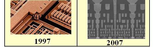
11 1950s Teal & Buehler Courtesy of Texas Instruments D. Edelstein, in P. Moon, et al., Intel Technology Journal 2, pp , 2008.
12 Chemical vapor deposition: Cu, Ir, Ru; Pt Plasma enhanced CVD processes: Cu Precipitation: Ni, Ru, Co, Pt, Pd Growth by desorption of Si from SiC X. Li et al, Science (2009). (Cu) P. Sutter et al., Physical Review B 80 (24) (2009). Pt N.A. Kholin et al., Surface Science (1984). Ir Karu and Beer, JAP (1966). Ni J. Sanchez-Barriga et al., Diamond and Related Materials (2010). Co J. Lee, et al, in IEDM - Technical Digest, (ICP-CVD) D. V. Badami, Nature (1962). SiC

 Ti/(C+Ti) T (K) T (K) Cu/(C+Cu) Precursor Sources: Gases Liquids Solids Solutions Ni/(C+Ni)")
13 Substrate t selection Metal C solubility Orientation Catalytic activity Lattice matched Dielectrics High-k, low-k? Layered compounds Process type: Growth Temperature Cold wall Hot wall Pressure Low Atmospheric (K) T T (K) Ti/(C+Ti) T (K) T (K) Cu/(C+Cu) Precursor Sources: Gases Liquids Solids Solutions Ni/(C+Ni) Ir/(C+Ir) Okamoto H., Phase Diagrams for Binary Alloys, Desk Handbook, Vol. 1, 2000
14 We can grow large area graphene Large area low defect density single crystals of graphene are most likely required to achieve the highest uniform transport properties for nano-electronic devices Can large single crystals of graphene be grown? Do we have the right substrate? Is the growth rate high enough for commercial viability? 2-D growth from a single nucleus? Can registered nuclei of graphene be created for further graphene large area crystal growth?


 10 m G. B.")


15 SEM TEM graphene 20 m Cu Graphene e islands 5 m Li et at. Science, 2009 Cu Cu Su urface Cove erage (%) 10 m G. B mtorr 285 mtorr 560 mtorr 0Q. Yu et 1al., Nature Materials, Time (min)


16 Grain Structure of graphene by Electron Diffraction: >2000 ED patterns Raman Isotope labeling 10 m 5 m C. Floresca, UT Dallas unpublished data Li et al., Science, 2009


17 Li et al., JACS 2011 Li et al JACS 2011 Li et al Science 2009


18 Cu substrate Pt substrate 400 m Yan Z, ACS Nano mm Y.Hao Unpublished results UT Austin L. Gao et al Nat. Comm. (2012)
19 Nucleation Graphene nuclei CH 4 + H 2 Cu Graphene Graphene domain CH 4 + H 2 Domain Growth CHx coverage CASE I: Isolated nuclei CH 4 + H 2 CASE II: Multiple nuclei CH 4 + H 2 C x H y C x H y C x H y C x H y Constant growth rate with time Infinite it exposed catalyst t C x H y C x H y C x H y Varying growth rate Finite/decreasing exposed catalyst


 Pt Petrone")
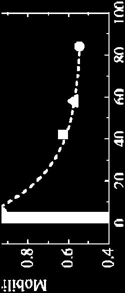
20 Mobility 16,400 25,000 cm2/v - for Gr/SiO 2 Mobility 27,000 45,000 cm2/v - for Gr/h-BN X. Li et al., Nano Letters (2010) Pt Petrone et al., Nano Letters (2012)


21 Very large area graphene can be grown on Cu and transferred to any substrate. PMMA Fe 3+ Acetone Si/SiO 2 Si/SiO 2 Li et al,. Nano Lett (2009) Bae et al. Nat. Nanotech. (2010)


 was")


22 Graphene grown and transferred multiple times from the same Cu foil An aqueous solution of K 2 S 2 O 8 (0.05 mm) was employed as electrolyte l t in the electrochemistry process. Wang, Y, ACS Nano 5(12), 927 (2011)


23 Single Crystal Graphene Exfoliated CVD Manchester UT Austin Shenyang UT Austin 1 m 1 mm Microns millimeters Centimeters meters Polycrystalline CVD Graphene UT Austin SKKU IBM Graphene Quartz 4 cm 23
24 Graphene surface is chemically inert Need to functionalize the surface to deposit dielectrics using non-physical deposition techniqueses Scaling of dielectrics down to ~ 1 nm needed for devices Enable a variety of dielectrics high-k, low-k and 2D dielectrics
 Standard ALD Al 2 O 3 processes (TMA/H 2 O) lead to non-uniform deposition at step edges Need to use a nucleation layer or Nucleation strategies for ALD on graphene Thin")

25 Y. Xuan, et al., APL 92, (2008) Standard ALD Al 2 O 3 processes (TMA/H 2 O) lead to non-uniform deposition at step edges Need to use a nucleation layer or Nucleation strategies for ALD on graphene Thin polymer (NFC CP) layer D. B. Farmer, et. al., Nano Lett. 9(12), 4474 (2009) 1 nm e-beam Al / oxidation in air S. Kim, et. al., APL 94, 6, (2009) D. B. Farmer, et. al., APL 97(1) (2010) Evaporated PTCDA M. Hersam et. al., in press. NO 2 noncovalent functionalization functionalize the graphene surface D. B. Farmer and R. G. Gordon, Nano Lett. 6(4), 699 (2006) Y.-M. Lin, et. al., Nano Lett. 9(1), 422 (2009) O 3 functionalization But, O 3 etches of HOPG surface at 200 C B. Lee, et. al., APL 92(20), (2008) GL G. Lee, et. al., J. JPhys.Chem. C 113(32), (2009) B. Lee, et. al., APL 97(4), (2010) G. Lee, et. Al., J.Phys. Chem. C 113, 32, (2009)

26 Pirkle, A, PhD Thesis, UT Dallas 2011 CVD graphene transferred to SiO 2 Main sp 2 graphene peak is fit with an asymmetric Doniach- Sunjic line FWHM for transferred graphene: 0.88 ev FWHM for CVD graphene on Cu: 0.74 ev PMMA residue observed after transfer (states highlighted in orange) Curve fit residual error shown below data in gray PMMA residue present PMMA fit is consistent with G. Beamson, et. al., Surface and Interface Analysis 17(2), 105 (1991)
 Al 2 O 3 1 nm (nominal) Al deposited by on natural graphite by e-beam evaporation,oxidized idi d in 1000 mbar O 2 at t25 C O 1s x10 x10 (d) (c) (b) (a) 536 532 528 C 1s * C-C (d) (c) (b) (a) 290")
 Al clusters explain incomplete oxidation when pre-deposition anneal is employed Cluster radius is larger than limiting oxide thickness (~ 0.")
27 eight (nm) He nm z RMS = 4.23 nm x ( m ) (a) Al Adsorbed H 2 O Al 2 O 3 Adsorbed H 2 O (b) Al Al 2 O 3 Al 17 nm 0 nm Pho otoelectro on intensit ty (a.u.) Al 2 O 3 1 nm (nominal) Al deposited by on natural graphite by e-beam evaporation,oxidized idi d in 1000 mbar O 2 at t25 C O 1s x10 x10 (d) (c) (b) (a) C 1s * C-C (d) (c) (b) (a) Binding energy (ev) Al 2p Al (d) (c) (b) (a) (d) + 25 C O 2 (c) Unannealed natural graphite substrate + 1 nm Al (b) + 25 C O 2 (a) Annealed (400 C, UHV) natural graphite substrate + 1 nm Al Large (~ 5-10 nm) Al clusters explain incomplete oxidation when pre-deposition anneal is employed Cluster radius is larger than limiting oxide thickness (~ nm) 1 Further details given in Ref L. P. H. Jeurgens, et. al., JAP 92, 3, 1649 (2002) 2. A. Pirkle, et. al, APL 95(13), (2009) 27
28 Hf 1s / O 1s fit regions 1: O 1s -HfO 2 2: O 1s - Hf(OH) 3: Hf 1s Pre-deposition anneal, deposition pressure 4x10⁻¹⁰ mbar necessary to suppress Hf carbide formation Hf 1s O1 1s C1 1s Hf 4f Pho otoelectro on intensit ty (a.u.) HfC (c) Annealed graphite, mbar deposition (LN 2 chamber shroud cooled) (b) Annealed graphite, mbar deposition (chamber shroud not cooled) (a) Exfoliated graphite, mbar deposition (chamber shroud not cooled) Binding energy (ev) A. Pirkle, et. al, APL 95(13), (2009)


 Photoele ectron intensit ty (a.u.")

 XPS No carbide detected after")


29 1 nm of HfO 2 deposited on natural graphite by evaporating Hf with 1x10⁻⁶ mbar partial pressure of O 2 in e-beam evaporation chamber Chamber base pressure 5x10⁻¹⁰ mbar Internal LN 2 chamber shroud cooled to minimize background residual gases (OH) Photoele ectron intensit ty (a.u.) O 1s C 1s Hf 4f 1 nm HfO 2 - reactive e-beam Natural graphite substrate AFM 1 nm HfO 2 on natural graphite Binding energy (ev) XPS No carbide detected after reactive e-beam deposition TEM 5 nm HfO 2 on natural graphite High and low magnification Low surface roughness: z rms = 0.24 nm Comparable to roughness of HfO 2 on Si spectator sample deposition images show good uniformity it (within a factor of ~2) No pinhole/short defects Pirkle, A, PhD Thesis, UT Dallas 2011 observed


30 2.2nm Oxidized Al 1.1nm 300nm 0 150nm 0 150nm 300nm 0 Oxidized Ti 2.2nm 1.1nm nm 300nm 0 150nm 300nm Provides nucleation centers for the ALD growth uniform coverage critical No detrimental effect on gate capacitance ultra-thin interfacial layer desirable Surface diffusion limits the minimum interfacial layer thickness B. Fallahazad et al. APL, 2012


31 Al 2 O 3 -TiO x dielectric on graphene scaled to ~ 2.6nm B. Fallahazad et al APL (2012) Are oxide high-k h kdielectrics ti good enough hto achieve high mobility in graphene?
 x ( m) Pirkle, A, PhD Thesis, UT Dallas 2011 Pho otoelectron in ntensity (cts/ /s) 18 x103 16 14 12 10 8 6 4 2 (f) (e) (g) (i) (h) (i) (h) (g) (e,f) (d) C 1s (c) (b) (a) 290 288")

32 Height (nm) CVD graphene transferred to SiO 2 using PMMA method Sample received in-situ 300 C / 3 hr vacuum anneal (P ~ 1x10⁻⁹ mbar) a) Transferred b) Annealed a) b) x ( m) x ( m) Pirkle, A, PhD Thesis, UT Dallas 2011 Pho otoelectron in ntensity (cts/ /s) 18 x (f) (e) (g) (i) (h) (i) (h) (g) (e,f) (d) C 1s (c) (b) (a) Binding energy (ev) c) Transferred CVD graphene on SiO C / 3 hr UHV anneal b) Transferred CVD graphene on SiO 2 C 1s XPS states corresponding to PMMA are largely removed AFM shows a much smoother surface RMS roughness drops from 4.6 nm to 0.6 nm upon annealing 300 C / 3 hr vacuum anneal is effective for significant removal of PMMA residue from graphene 0 a) CVD graphene on Cu
33 Chen J, ACS Nano, 2012
 Without Parylene With")
 (b) 3 Mobility ~ 5000 cm 2 /V s nce [K] Resista 2 1 0 6 0-6 nm V D = 10 mv")
34 Ni/Au Ni/Au Parylene Graphene SiO 2 (90 nm) Ni/Au (a) (b) Nickel Parylene ~7 nm 5nm Graphene n++ Si substrate 1 um 5 nm SiO 2 Intens sity cps (a) Without Parylene With Parylene Raman Shift (cm -1 ) Mordi et al., Appl. Phys. Lett. 100, (2012) (b) 3 Mobility ~ 5000 cm 2 /V s nce [K] Resista nm V D = 10 mv V BG [V]


 2 nm C.")


35 Exfoliated h-bn CVD FL h-bn CVD Monolayer h-bn Kim et al NL (2012) 2 nm C.R. Dean et al, Nature Nanotech, 2010 Ismach et al, ACS Nano accepted for pub
36 C 1s 1.0 PI (a.u.) HOPG + 1 nm Ni+ 500 C / 10 min anneal (UHV) HOPG + 1 nm Ni HOPG I d (ma) μm V bg (V) BE ( ev ) V d (V) XPS analysis indicates absence of carbide formation ( ~ 282 ev) at the Ni graphene interface I d -V d plots for Ni on graphene indicative of ohmic behavior higher total resistance (R) and hence higher R c A. Venugopal, Ph.D. Thesis, UT Dallas, 2012
37 Exfoliated 2 CVD grown CVD Graphene R c (k) 1 old transfer new transfer TiO x process L c = 3m W c (m) ~ 5X reduction in R c observed Residue at interface significantly contributes to R c A. Venugopal, Ph.D. Thesis, UT Dallas, 2012
38 Progress has been made in graphene growth and integration of graphene-based devices Large area polycrystalline CVD graphene Large, g a few mm, single crystal graphene Many issues remain on uniformity/roughness Need to improve contacts Scaling of dielectrics to 1 nm range H-BN shows promise but growth of reproducible uniform films is still very challenging
Luigi Colombo. Texas Instruments Dallas, TX, USA. Jozef Stefan Institute Ljubljana, Slovenia April 9, 2013
 Luigi Colombo Texas Instruments Dallas, TX, USA Jozef Stefan Institute Ljubljana, Slovenia April 9, 2013 UT Austin Ruoff group UT Austin - Banerjee group UT Austin - Tutuc group UT Dallas - Wallace group
Graphene devices and integration: A primer on challenges
 Graphene devices and integration: A primer on challenges Archana Venugopal (TI) 8 Nov 2016 Acknowledgments: Luigi Colombo (TI) UT Dallas and UT Austin 1 Outline Where we are Issues o Contact resistance
Supplementary Figure S1. AFM characterizations and topographical defects of h- BN films on silica substrates. (a) (c) show the AFM height
 (c) show the AFM height") Supplementary Figure S1. AFM characterizations and topographical defects of h- BN films on silica substrates. (a) (c) show the AFM height topographies of h-bn film in a size of ~1.5µm 1.5µm, 30µm 30µm
Supplementary Figure S1. AFM characterizations and topographical defects of h- BN films on silica substrates. (a) (c) show the AFM height topographies of h-bn film in a size of ~1.5µm 1.5µm, 30µm 30µm
Evolution of graphene growth on Cu and Ni studied by carbon isotope
 Evolution of graphene growth on Cu and Ni studied by carbon isotope labeling Xuesong Li a, Weiwei Cai a, Luigi Colombo b*, and Rodney S. Ruoff a* Large-area graphene is a new material with properties that
Supplementary Figure S1. AFM images of GraNRs grown with standard growth process. Each of these pictures show GraNRs prepared independently,
 Supplementary Figure S1. AFM images of GraNRs grown with standard growth process. Each of these pictures show GraNRs prepared independently, suggesting that the results is reproducible. Supplementary Figure
Optimizing Graphene Morphology on SiC(0001)
") Optimizing Graphene Morphology on SiC(0001) James B. Hannon Rudolf M. Tromp Graphene sheets Graphene sheets can be formed into 0D,1D, 2D, and 3D structures Chemically inert Intrinsically high carrier mobility
Optimizing Graphene Morphology on SiC(0001) James B. Hannon Rudolf M. Tromp Graphene sheets Graphene sheets can be formed into 0D,1D, 2D, and 3D structures Chemically inert Intrinsically high carrier mobility
A new method of growing graphene on Cu by hydrogen etching
 A new method of growing graphene on Cu by hydrogen etching Linjie zhan version 6, 2015.05.12--2015.05.24 CVD graphene Hydrogen etching Anisotropic Copper-catalyzed Highly anisotropic hydrogen etching method
SUPPLEMENTARY INFORMATION
 SUPPLEMENTARY INFORMATION Facile Synthesis of High Quality Graphene Nanoribbons Liying Jiao, Xinran Wang, Georgi Diankov, Hailiang Wang & Hongjie Dai* Supplementary Information 1. Photograph of graphene
SUPPLEMENTARY INFORMATION. Observation of tunable electrical bandgap in large-area twisted bilayer graphene synthesized by chemical vapor deposition
 SUPPLEMENTARY INFORMATION Observation of tunable electrical bandgap in large-area twisted bilayer graphene synthesized by chemical vapor deposition Jing-Bo Liu 1 *, Ping-Jian Li 1 *, Yuan-Fu Chen 1, Ze-Gao
Supporting Information
 Electronic Supplementary Material (ESI) for ChemComm. This journal is The Royal Society of Chemistry 2014 Supporting Information Controllable Atmospheric Pressure Growth of Mono-layer, Bi-layer and Tri-layer
Wafer Scale Homogeneous Bilayer Graphene Films by. Chemical Vapor Deposition
 Supporting Information for Wafer Scale Homogeneous Bilayer Graphene Films by Chemical Vapor Deposition Seunghyun Lee, Kyunghoon Lee, Zhaohui Zhong Department of Electrical Engineering and Computer Science,
Graphene films on silicon carbide (SiC) wafers supplied by Nitride Crystals, Inc.
 wafers supplied by Nitride Crystals, Inc.") 9702 Gayton Road, Suite 320, Richmond, VA 23238, USA Phone: +1 (804) 709-6696 info@nitride-crystals.com www.nitride-crystals.com Graphene films on silicon carbide (SiC) wafers supplied by Nitride Crystals,
9702 Gayton Road, Suite 320, Richmond, VA 23238, USA Phone: +1 (804) 709-6696 info@nitride-crystals.com www.nitride-crystals.com Graphene films on silicon carbide (SiC) wafers supplied by Nitride Crystals,
Fabrication Technology, Part I
 EEL5225: Principles of MEMS Transducers (Fall 2004) Fabrication Technology, Part I Agenda: Microfabrication Overview Basic semiconductor devices Materials Key processes Oxidation Thin-film Deposition Reading:
Supporting Information. Fast Synthesis of High-Performance Graphene by Rapid Thermal Chemical Vapor Deposition
 1 Supporting Information Fast Synthesis of High-Performance Graphene by Rapid Thermal Chemical Vapor Deposition Jaechul Ryu, 1,2, Youngsoo Kim, 4, Dongkwan Won, 1 Nayoung Kim, 1 Jin Sung Park, 1 Eun-Kyu
A. Optimizing the growth conditions of large-scale graphene films
 1 A. Optimizing the growth conditions of large-scale graphene films Figure S1. Optical microscope images of graphene films transferred on 300 nm SiO 2 /Si substrates. a, Images of the graphene films grown
Supporting Information
 Supporting Information Repeated Growth Etching Regrowth for Large-Area Defect-Free Single-Crystal Graphene by Chemical Vapor Deposition Teng Ma, 1 Wencai Ren, 1 * Zhibo Liu, 1 Le Huang, 2 Lai-Peng Ma,
Supplementary Information for
 Supplementary Information for Highly Stable, Dual-Gated MoS 2 Transistors Encapsulated by Hexagonal Boron Nitride with Gate-Controllable Contact Resistance and Threshold Voltage Gwan-Hyoung Lee, Xu Cui,
Supplementary Information
 Supplementary Information Plasma-assisted reduction of graphene oxide at low temperature and atmospheric pressure for flexible conductor applications Seung Whan Lee 1, Cecilia Mattevi 2, Manish Chhowalla
Graphene Growth and Device Integration
 INVITED PAPER Graphene Growth and Device Integration This paper describes one of the emerging methods for growing graphenevthe chemical vapor deposition methodvwhich is based on a catalytic reaction between
Spin-Conserving Resonant Tunneling in Twist- Supporting Information
 Spin-Conserving Resonant Tunneling in Twist- Controlled WSe2-hBN-WSe2 Heterostructures Supporting Information Kyounghwan Kim, 1 Nitin Prasad, 1 Hema C. P. Movva, 1 G. William Burg, 1 Yimeng Wang, 1 Stefano
Supplementary Figure 1 Experimental setup for crystal growth. Schematic drawing of the experimental setup for C 8 -BTBT crystal growth.
 Supplementary Figure 1 Experimental setup for crystal growth. Schematic drawing of the experimental setup for C 8 -BTBT crystal growth. Supplementary Figure 2 AFM study of the C 8 -BTBT crystal growth
Chapter 2 Synthesis, Structure, and Properties of Graphene and Graphene Oxide
 Chapter 2 Synthesis, Structure, and Properties of Graphene and Graphene Oxide 2.1 Introduction To develop large-area graphene-based TCFs, one of the foremost challenges is to produce sufficient amounts
Scaling up Chemical Vapor Deposition Graphene to 300 mm Si substrates
 Scaling up Chemical Vapor Deposition Graphene to 300 mm Si substrates Co- Authors Aixtron Alex Jouvray Simon Buttress Gavin Dodge Ken Teo The work shown here has received partial funding from the European
crystals were phase-pure as determined by x-ray diffraction. Atomically thin MoS 2 flakes were
 Nano Letters (214) Supplementary Information for High Mobility WSe 2 p- and n-type Field Effect Transistors Contacted by Highly Doped Graphene for Low-Resistance Contacts Hsun-Jen Chuang, Xuebin Tan, Nirmal
Supplementary Information for. Origin of New Broad Raman D and G Peaks in Annealed Graphene
 Supplementary Information for Origin of New Broad Raman D and G Peaks in Annealed Graphene Jinpyo Hong, Min Kyu Park, Eun Jung Lee, DaeEung Lee, Dong Seok Hwang and Sunmin Ryu* Department of Applied Chemistry,
Supplementary Figures Supplementary Figure 1
 Supplementary Figures Supplementary Figure 1 Optical images of graphene grains on Cu after Cu oxidation treatment at 200 for 1m 30s. Each sample was synthesized with different H 2 annealing time for (a)
NiCl2 Solution concentration. Etching Duration. Aspect ratio. Experiment Atmosphere Temperature. Length(µm) Width (nm) Ar:H2=9:1, 150Pa
 Width (nm) Ar:H2=9:1, 150Pa") Experiment Atmosphere Temperature #1 # 2 # 3 # 4 # 5 # 6 # 7 # 8 # 9 # 10 Ar:H2=9:1, 150Pa Ar:H2=9:1, 150Pa Ar:H2=9:1, 150Pa Ar:H2=9:1, 150Pa Ar:H2=9:1, 150Pa Ar:H2=9:1, 150Pa Ar:H2=9:1, 150Pa Ar:H2=9:1,
Experiment Atmosphere Temperature #1 # 2 # 3 # 4 # 5 # 6 # 7 # 8 # 9 # 10 Ar:H2=9:1, 150Pa Ar:H2=9:1, 150Pa Ar:H2=9:1, 150Pa Ar:H2=9:1, 150Pa Ar:H2=9:1, 150Pa Ar:H2=9:1, 150Pa Ar:H2=9:1, 150Pa Ar:H2=9:1,
ALD high-k and higher-k integration on GaAs
 ALD high-k and higher-k integration on GaAs Ozhan Koybasi 1), Min Xu 1), Yiqun Liu 2), Jun-Jieh Wang 2), Roy G. Gordon 2), and Peide D. Ye 1)* 1) School of Electrical and Computer Engineering, Purdue University,
Supplementary Figure 1 Dark-field optical images of as prepared PMMA-assisted transferred CVD graphene films on silicon substrates (a) and the one
 and the one") Supplementary Figure 1 Dark-field optical images of as prepared PMMA-assisted transferred CVD graphene films on silicon substrates (a) and the one after PBASE monolayer growth (b). 1 Supplementary Figure
Supplementary Figure 1 Dark-field optical images of as prepared PMMA-assisted transferred CVD graphene films on silicon substrates (a) and the one after PBASE monolayer growth (b). 1 Supplementary Figure
SUPPLEMENTARY INFORMATION
 doi:.38/nature09979 I. Graphene material growth and transistor fabrication Top-gated graphene RF transistors were fabricated based on chemical vapor deposition (CVD) grown graphene on copper (Cu). Cu foil
Layer-modulated synthesis of uniform tungsten disulfide nanosheet using gas-phase precursors.
 Layer-modulated synthesis of uniform tungsten disulfide nanosheet using gas-phase precursors. Jusang Park * Hyungjun Kim School of Electrical and Electronics Engineering, Yonsei University, 262 Seongsanno,
Wafer-Scale Single-Domain-Like Graphene by. Defect-Selective Atomic Layer Deposition of
 Electronic Supplementary Material (ESI) for Nanoscale. This journal is The Royal Society of Chemistry 2015 Wafer-Scale Single-Domain-Like Graphene by Defect-Selective Atomic Layer Deposition of Hexagonal
Figure 1: Graphene release, transfer and stacking processes. The graphene stacking began with CVD
 Supplementary figure 1 Graphene Growth and Transfer Graphene PMMA FeCl 3 DI water Copper foil CVD growth Back side etch PMMA coating Copper etch in 0.25M FeCl 3 DI water rinse 1 st transfer DI water 1:10
Supplementary Information
 Supplementary Information Supplementary Figure 1. fabrication. A schematic of the experimental setup used for graphene Supplementary Figure 2. Emission spectrum of the plasma: Negative peaks indicate an
Large Scale Direct Synthesis of Graphene on Sapphire and Transfer-free Device Fabrication
 Supplementary Information Large Scale Direct Synthesis of Graphene on Sapphire and Transfer-free Device Fabrication Hyun Jae Song a, Minhyeok Son a, Chibeom Park a, Hyunseob Lim a, Mark P. Levendorf b,
CVD growth of Graphene. SPE ACCE presentation Carter Kittrell James M. Tour group September 9 to 11, 2014
 CVD growth of Graphene SPE ACCE presentation Carter Kittrell James M. Tour group September 9 to 11, 2014 Graphene zigzag armchair History 1500: Pencil-Is it made of lead? 1789: Graphite 1987: The first
Special Properties of Au Nanoparticles
 Special Properties of Au Nanoparticles Maryam Ebrahimi Chem 7500/750 March 28 th, 2007 1 Outline Introduction The importance of unexpected electronic, geometric, and chemical properties of nanoparticles
CVD: General considerations.
 CVD: General considerations. PVD: Move material from bulk to thin film form. Limited primarily to metals or simple materials. Limited by thermal stability/vapor pressure considerations. Typically requires
Emerging Interconnect Technologies for CMOS and beyond-cmos Circuits
 Emerging Interconnect Technologies for CMOS and beyond-cmos Circuits Sou-Chi Chang, Rouhollah M. Iraei Vachan Kumar, Ahmet Ceyhan and Azad Naeemi School of Electrical & Computer Engineering Georgia Institute
Supporting information
 Supporting information Design, Modeling and Fabrication of CVD Grown MoS 2 Circuits with E-Mode FETs for Large-Area Electronics Lili Yu 1*, Dina El-Damak 1*, Ujwal Radhakrishna 1, Xi Ling 1, Ahmad Zubair
Supporting Data. The University of Texas at Dallas, 800 West Campbell Road, Richardson, Texas 75080, United
 Supporting Data MoS 2 Functionalization for Ultra-thin Atomic Layer Deposited Dielectrics Angelica Azcatl, 1 Stephen McDonnell, 1 Santosh KC, 1 Xing Peng, 1 Hong Dong, 1 Xiaoye Qin, 1 Rafik Addou, 1 Greg
Supplementary Figures
 Supplementary Figures 1500 Heating Annealing Growing Cooling 20 Temperature ( o C) 1000 500 Ar:H 2 = 5:1 Ar:H 2 = 5:1 15 10 5 Pressure(Pa) 0 Ar(SiH 4 (5%)):C 2 H 2 = 1:2 120 mins 5 mins 5 40 mins ~120
Supporting Information
 Supporting Information Direct Chemical Vapor Deposition-Derived Graphene Glasses Targeting Wide Ranged Applications Jingyu Sun, Yubin Chen, Manish Kr. Priydarshi, Zhang Chen, Alicja Bachmatiuk,, Zhiyu
Hopping in CVD Grown Single-layer MoS 2
 Supporting Information for Large Thermoelectricity via Variable Range Hopping in CVD Grown Single-layer MoS 2 Jing Wu 1,2,3, Hennrik Schmidt 1,2, Kiran Kumar Amara 4, Xiangfan Xu 5, Goki Eda 1,2,4, and
Introduction to Nanotechnology Chapter 5 Carbon Nanostructures Lecture 1
 Introduction to Nanotechnology Chapter 5 Carbon Nanostructures Lecture 1 ChiiDong Chen Institute of Physics, Academia Sinica chiidong@phys.sinica.edu.tw 02 27896766 Carbon contains 6 electrons: (1s) 2,
ConceptGraphene. Small or medium-scale focused research project. WP1 Fabrication
 ConceptGraphene New Electronics Concept: Wafer-Scale Epitaxial Graphene Small or medium-scale focused research project WP1 Fabrication Deliverable 1.2 Quality comparison: epitaxial graphene vs graphene
Wafer-scale fabrication of graphene
 Wafer-scale fabrication of graphene Sten Vollebregt, MSc Delft University of Technology, Delft Institute of Mircosystems and Nanotechnology Delft University of Technology Challenge the future Delft University
GHZ ELECTRICAL PROPERTIES OF CARBON NANOTUBES ON SILICON DIOXIDE MICRO BRIDGES
 GHZ ELECTRICAL PROPERTIES OF CARBON NANOTUBES ON SILICON DIOXIDE MICRO BRIDGES SHENG F. YEN 1, HAROON LAIS 1, ZHEN YU 1, SHENGDONG LI 1, WILLIAM C. TANG 1,2, AND PETER J. BURKE 1,2 1 Electrical Engineering
ALD Nucleation and Area-Selective Deposition
 ALD Nucleation and Area-Selective Deposition Prof Gregory N. Parsons Department of Chemical and Biomolecular Engineering North Carolina State University Raleigh North Carolina USA 1 Outline 1. Nucleation
Hydrogenation of Single Walled Carbon Nanotubes
 Hydrogenation of Single Walled Carbon Nanotubes Anders Nilsson Stanford Synchrotron Radiation Laboratory (SSRL) and Stockholm University Coworkers and Ackowledgement A. Nikitin 1), H. Ogasawara 1), D.
Center for Integrated Nanostructure Physics (CINAP)
") Center for Integrated Nanostructure Physics (CINAP) - Institute for Basic Science (IBS) was launched in 2012 by the Korean government to promote basic science in Korea - Our Center was established in 2012
Center for Integrated Nanostructure Physics (CINAP) - Institute for Basic Science (IBS) was launched in 2012 by the Korean government to promote basic science in Korea - Our Center was established in 2012
3.155J/6.152J Microelectronic Processing Technology Fall Term, 2004
 3.155J/6.152J Microelectronic Processing Technology Fall Term, 2004 Bob O'Handley Martin Schmidt Quiz Nov. 17, 2004 Ion implantation, diffusion [15] 1. a) Two identical p-type Si wafers (N a = 10 17 cm
Low Temperature Plasma CVD Grown Graphene by Microwave Surface-Wave Plasma CVD Using Camphor Precursor
 Journal of Physical Science and Application 6 (2) (2016) 34-38 doi: 10.17265/2159-5348/2016.02.005 D DAVID PUBLISHING Low Temperature Plasma CVD Grown Graphene by Microwave Surface-Wave Plasma CVD Using
Supporting Online Material for
 www.sciencemag.org/cgi/content/full/327/5966/662/dc Supporting Online Material for 00-GHz Transistors from Wafer-Scale Epitaxial Graphene Y.-M. Lin,* C. Dimitrakopoulos, K. A. Jenkins, D. B. Farmer, H.-Y.
High speed vacuum deposition of organic TFTs in a roll-to-roll facility
 High speed vacuum deposition of organic TFTs in a roll-to-roll facility Dr Hazel Assender University of Oxford 1 Prof Martin Taylor Eifion Patchett, Aled Williams Prof Long Lin Prof Steve Yeates Dr John
Surface Defects on Natural MoS 2
 Supporting Information: Surface Defects on Natural MoS 2 Rafik Addou 1*, Luigi Colombo 2, and Robert M. Wallace 1* 1 Department of Materials Science and Engineering, The University of Texas at Dallas,
Chemical vapor deposition (CVD) techniques have been
 techniques have been") pubs.acs.org/nanolett Growth of Adlayer Graphene on Cu Studied by Carbon Isotope Labeling Qiongyu Li, Harry Chou, Jin-Hui Zhong, Jun-Yang Liu, Andrei Dolocan, Junyan Zhang, Yinghui Zhou, Rodney S. Ruoff,
pubs.acs.org/nanolett Growth of Adlayer Graphene on Cu Studied by Carbon Isotope Labeling Qiongyu Li, Harry Chou, Jin-Hui Zhong, Jun-Yang Liu, Andrei Dolocan, Junyan Zhang, Yinghui Zhou, Rodney S. Ruoff,
Supporting Information for: Sustained sub-60 mv/decade switching via the negative capacitance effect in MoS 2 transistors
 Supporting Information for: Sustained sub-60 mv/decade switching via the negative capacitance effect in MoS 2 transistors Felicia A. McGuire 1, Yuh-Chen Lin 1, Katherine Price 1, G. Bruce Rayner 2, Sourabh
A Novel Approach to the Layer Number-Controlled and Grain Size- Controlled Growth of High Quality Graphene for Nanoelectronics
 Supporting Information A Novel Approach to the Layer Number-Controlled and Grain Size- Controlled Growth of High Quality Graphene for Nanoelectronics Tej B. Limbu 1,2, Jean C. Hernández 3, Frank Mendoza
The goal of this project is to enhance the power density and lowtemperature efficiency of solid oxide fuel cells (SOFC) manufactured by atomic layer
 manufactured by atomic layer") Stanford University Michael Shandalov1, Shriram Ramanathan2, Changhyun Ko2 and Paul McIntyre1 1Department of Materials Science and Engineering, Stanford University 2Division of Engineering and Applied
Stanford University Michael Shandalov1, Shriram Ramanathan2, Changhyun Ko2 and Paul McIntyre1 1Department of Materials Science and Engineering, Stanford University 2Division of Engineering and Applied
Fermi Level Pinning at Electrical Metal Contacts. of Monolayer Molybdenum Dichalcogenides
 Supporting information Fermi Level Pinning at Electrical Metal Contacts of Monolayer Molybdenum Dichalcogenides Changsik Kim 1,, Inyong Moon 1,, Daeyeong Lee 1, Min Sup Choi 1, Faisal Ahmed 1,2, Seunggeol
XPS/UPS and EFM. Brent Gila. XPS/UPS Ryan Davies EFM Andy Gerger
 XPS/UPS and EFM Brent Gila XPS/UPS Ryan Davies EFM Andy Gerger XPS/ESCA X-ray photoelectron spectroscopy (XPS) also called Electron Spectroscopy for Chemical Analysis (ESCA) is a chemical surface analysis
Effects of plasma treatment on the precipitation of fluorine-doped silicon oxide
 ARTICLE IN PRESS Journal of Physics and Chemistry of Solids 69 (2008) 555 560 www.elsevier.com/locate/jpcs Effects of plasma treatment on the precipitation of fluorine-doped silicon oxide Jun Wu a,, Ying-Lang
Hydrogenated Graphene
 Hydrogenated Graphene Stefan Heun NEST, Istituto Nanoscienze-CNR and Scuola Normale Superiore Pisa, Italy Outline Epitaxial Graphene Hydrogen Chemisorbed on Graphene Hydrogen-Intercalated Graphene Outline
Supplementary Figure S1. AFM image and height profile of GO. (a) AFM image
 AFM image") Supplementary Figure S1. AFM image and height profile of GO. (a) AFM image and (b) height profile of GO obtained by spin-coating on silicon wafer, showing a typical thickness of ~1 nm. 1 Supplementary
Supplementary Figure S1. AFM image and height profile of GO. (a) AFM image and (b) height profile of GO obtained by spin-coating on silicon wafer, showing a typical thickness of ~1 nm. 1 Supplementary
2D Materials for Gas Sensing
 2D Materials for Gas Sensing S. Guo, A. Rani, and M.E. Zaghloul Department of Electrical and Computer Engineering The George Washington University, Washington DC 20052 Outline Background Structures of
Graphene Fundamentals and Emergent Applications
 Graphene Fundamentals and Emergent Applications Jamie H. Warner Department of Materials University of Oxford Oxford, UK Franziska Schaffel Department of Materials University of Oxford Oxford, UK Alicja
Graphene: Plane and Simple Electrical Metrology?
 Graphene: Plane and Simple Electrical Metrology? R. E. Elmquist, F. L. Hernandez-Marquez, M. Real, T. Shen, D. B. Newell, C. J. Jacob, and G. R. Jones, Jr. National Institute of Standards and Technology,
Stretching the Barriers An analysis of MOSFET Scaling. Presenters (in order) Zeinab Mousavi Stephanie Teich-McGoldrick Aseem Jain Jaspreet Wadhwa
 Zeinab Mousavi Stephanie Teich-McGoldrick Aseem Jain Jaspreet Wadhwa") Stretching the Barriers An analysis of MOSFET Scaling Presenters (in order) Zeinab Mousavi Stephanie Teich-McGoldrick Aseem Jain Jaspreet Wadhwa Why Small? Higher Current Lower Gate Capacitance Higher
Stretching the Barriers An analysis of MOSFET Scaling Presenters (in order) Zeinab Mousavi Stephanie Teich-McGoldrick Aseem Jain Jaspreet Wadhwa Why Small? Higher Current Lower Gate Capacitance Higher
Steep-slope WSe 2 Negative Capacitance Field-effect Transistor
 Supplementary Information for: Steep-slope WSe 2 Negative Capacitance Field-effect Transistor Mengwei Si, Chunsheng Jiang, Wonil Chung, Yuchen Du, Muhammad A. Alam, and Peide D. Ye School of Electrical
Low Frequency Noise in MoS 2 Negative Capacitance Field-effect Transistor
 Low Frequency Noise in MoS Negative Capacitance Field-effect Transistor Sami Alghamdi, Mengwei Si, Lingming Yang, and Peide D. Ye* School of Electrical and Computer Engineering Purdue University West Lafayette,
TRANSVERSE SPIN TRANSPORT IN GRAPHENE
 International Journal of Modern Physics B Vol. 23, Nos. 12 & 13 (2009) 2641 2646 World Scientific Publishing Company TRANSVERSE SPIN TRANSPORT IN GRAPHENE TARIQ M. G. MOHIUDDIN, A. A. ZHUKOV, D. C. ELIAS,
Photoresist Profile. Undercut: negative slope, common for negative resist; oxygen diffusion prohibits cross-linking; good for lift-off.
 Photoresist Profile 4-15 Undercut: negative slope, common for negative resist; oxygen diffusion prohibits cross-linking; good for lift-off undercut overcut Overcut: positive slope, common to positive resist,
STM and graphene. W. W. Larry Pai ( 白偉武 ) Center for condensed matter sciences, National Taiwan University NTHU, 2013/05/23
 Center for condensed matter sciences, National Taiwan University NTHU, 2013/05/23") STM and graphene W. W. Larry Pai ( 白偉武 ) Center for condensed matter sciences, National Taiwan University NTHU, 2013/05/23 Why graphene is important: It is a new form of material (two dimensional, single
STM and graphene W. W. Larry Pai ( 白偉武 ) Center for condensed matter sciences, National Taiwan University NTHU, 2013/05/23 Why graphene is important: It is a new form of material (two dimensional, single
Supporting Information. by Hexagonal Boron Nitride
 Supporting Information High Velocity Saturation in Graphene Encapsulated by Hexagonal Boron Nitride Megan A. Yamoah 1,2,, Wenmin Yang 1,3, Eric Pop 4,5,6, David Goldhaber-Gordon 1 * 1 Department of Physics,
Atmospheric pressure Plasma Enhanced CVD for large area deposition of TiO 2-x electron transport layers for PV. Heather M. Yates
 Atmospheric pressure Plasma Enhanced CVD for large area deposition of TiO 2-x electron transport layers for PV Heather M. Yates Why the interest? Perovskite solar cells have shown considerable promise
Thermal Transport in Graphene and other Two-Dimensional Systems. Li Shi. Department of Mechanical Engineering & Texas Materials Institute
 Thermal Transport in Graphene and other Two-Dimensional Systems Li Shi Department of Mechanical Engineering & Texas Materials Institute Outline Thermal Transport Theories and Simulations of Graphene Raman
Electronics with 2D Crystals: Scaling extender, or harbinger of new functions?
 Electronics with 2D Crystals: Scaling extender, or harbinger of new functions? 1 st Workshop on Data Abundant Systems Technology Stanford, April 2014 Debdeep Jena (djena@nd.edu) Electrical Engineering,
Understanding Irreducible and Reducible Oxides as Catalysts for Carbon Nanotubes and Graphene Formation
 Wright State University CORE Scholar Special Session 5: Carbon and Oxide Based Nanostructured Materials (2011) Special Session 5 6-2011 Understanding Irreducible and Reducible Oxides as Catalysts for Carbon
Graphene Novel Material for Nanoelectronics
 Graphene Novel Material for Nanoelectronics Shintaro Sato Naoki Harada Daiyu Kondo Mari Ohfuchi (Manuscript received May 12, 2009) Graphene is a flat monolayer of carbon atoms with a two-dimensional honeycomb
Recap (so far) Low-Dimensional & Boundary Effects
 Low-Dimensional & Boundary Effects") Recap (so far) Ohm s & Fourier s Laws Mobility & Thermal Conductivity Heat Capacity Wiedemann-Franz Relationship Size Effects and Breakdown of Classical Laws 1 Low-Dimensional & Boundary Effects Energy
Recap (so far) Ohm s & Fourier s Laws Mobility & Thermal Conductivity Heat Capacity Wiedemann-Franz Relationship Size Effects and Breakdown of Classical Laws 1 Low-Dimensional & Boundary Effects Energy
Supporting Information
 Supporting Information Monolithically Integrated Flexible Black Phosphorus Complementary Inverter Circuits Yuanda Liu, and Kah-Wee Ang* Department of Electrical and Computer Engineering National University
Electrochemically Exfoliated Graphene as Solution-Processable, Highly-Conductive Electrodes for Organic Electronics
 Supporting Information Electrochemically Exfoliated Graphene as Solution-Processable, Highly-Conductive Electrodes for Organic Electronics Khaled Parvez, Rongjin Li, Sreenivasa Reddy Puniredd, Yenny Hernandez,
Supporting Information
 Electronic Supplementary Material (ESI) for Journal of Materials Chemistry C. This journal is The Royal Society of Chemistry 2018 Supporting Information Direct Integration of Polycrystalline Graphene on
Supplementary information for Nonvolatile Memory Cells Based on MoS 2 /Graphene Heterostructures
 Supplementary information for Nonvolatile Memory Cells Based on MoS 2 /Graphene Heterostructures Simone Bertolazzi, Daria Krasnozhon, Andras Kis * Electrical Engineering Institute, École Polytechnique
DEPOSITION OF THIN TiO 2 FILMS BY DC MAGNETRON SPUTTERING METHOD
 Chapter 4 DEPOSITION OF THIN TiO 2 FILMS BY DC MAGNETRON SPUTTERING METHOD 4.1 INTRODUCTION Sputter deposition process is another old technique being used in modern semiconductor industries. Sputtering
Nanostructure. Materials Growth Characterization Fabrication. More see Waser, chapter 2
 Nanostructure Materials Growth Characterization Fabrication More see Waser, chapter 2 Materials growth - deposition deposition gas solid Physical Vapor Deposition Chemical Vapor Deposition Physical Vapor
An account of our efforts towards air quality monitoring in epitaxial graphene on SiC
 European Network on New Sensing Technologies for Air Pollution Control and Environmental Sustainability - EuNetAir COST Action TD1105 2 nd International Workshop EuNetAir on New Sensing Technologies for
Graphene. Tianyu Ye November 30th, 2011
 Graphene Tianyu Ye November 30th, 2011 Outline What is graphene? How to make graphene? (Exfoliation, Epitaxial, CVD) Is it graphene? (Identification methods) Transport properties; Other properties; Applications;
Photovoltaic Enhancement Due to Surface-Plasmon Assisted Visible-Light. Absorption at the Inartificial Surface of Lead Zirconate-Titanate Film
 Photovoltaic Enhancement Due to Surface-Plasmon Assisted Visible-Light Absorption at the Inartificial Surface of Lead Zirconate-Titanate Film Fengang Zheng, a,b, * Peng Zhang, a Xiaofeng Wang, a Wen Huang,
Nova 600 NanoLab Dual beam Focused Ion Beam IITKanpur
 Nova 600 NanoLab Dual beam Focused Ion Beam system @ IITKanpur Dual Beam Nova 600 Nano Lab From FEI company (Dual Beam = SEM + FIB) SEM: The Electron Beam for SEM Field Emission Electron Gun Energy : 500
Intrinsic Electronic Transport Properties of High. Information
 Intrinsic Electronic Transport Properties of High Quality and MoS 2 : Supporting Information Britton W. H. Baugher, Hugh O. H. Churchill, Yafang Yang, and Pablo Jarillo-Herrero Department of Physics, Massachusetts
Multicolor Graphene Nanoribbon/Semiconductor Nanowire. Heterojunction Light-Emitting Diodes
 Multicolor Graphene Nanoribbon/Semiconductor Nanowire Heterojunction Light-Emitting Diodes Yu Ye, a Lin Gan, b Lun Dai, *a Hu Meng, a Feng Wei, a Yu Dai, a Zujin Shi, b Bin Yu, a Xuefeng Guo, b and Guogang
Initial Stages of Growth of Organic Semiconductors on Graphene
 Initial Stages of Growth of Organic Semiconductors on Graphene Presented by: Manisha Chhikara Supervisor: Prof. Dr. Gvido Bratina University of Nova Gorica Outline Introduction to Graphene Fabrication
EE143 Fall 2016 Microfabrication Technologies. Lecture 6: Thin Film Deposition Reading: Jaeger Chapter 6
 EE143 Fall 2016 Microfabrication Technologies Lecture 6: Thin Film Deposition Reading: Jaeger Chapter 6 Prof. Ming C. Wu wu@eecs.berkeley.edu 511 Sutardja Dai Hall (SDH) 1 Vacuum Basics Units 1 atmosphere
SUPPLEMENTARY INFORMATION
 Effect of airborne contaminants on the wettability of supported graphene and graphite Zhiting Li 1,ǂ, Yongjin Wang 2, ǂ, Andrew Kozbial 2, Ganesh Shenoy 1, Feng Zhou 1, Rebecca McGinley 2, Patrick Ireland
Towards Graphene-based heterojunction devices for microelectronic applications
 Towards Graphene-based heterojunction devices for microelectronic applications IHP GmbH Leibniz (Innovations for High Performance Microelectronics) TU-Dresden/IHM (Institute of Semiconductors and Microsystems)
Carbon Nanotubes in Interconnect Applications
 Carbon Nanotubes in Interconnect Applications Page 1 What are Carbon Nanotubes? What are they good for? Why are we interested in them? - Interconnects of the future? Comparison of electrical properties
LECTURE 5 SUMMARY OF KEY IDEAS
 LECTURE 5 SUMMARY OF KEY IDEAS Etching is a processing step following lithography: it transfers a circuit image from the photoresist to materials form which devices are made or to hard masking or sacrificial
Nanocarbon Technology for Development of Innovative Devices
 Nanocarbon Technology for Development of Innovative Devices Shintaro Sato Daiyu Kondo Shinichi Hirose Junichi Yamaguchi Graphene, a one-atom-thick honeycomb lattice made of carbon, and a carbon nanotube,