Graphene: Plane and Simple Electrical Metrology?
|
|
|
- Jeffry Tucker
- 5 years ago
- Views:
Transcription

1 Graphene: Plane and Simple Electrical Metrology? R. E. Elmquist, F. L. Hernandez-Marquez, M. Real, T. Shen, D. B. Newell, C. J. Jacob, and G. R. Jones, Jr. National Institute of Standards and Technology, Gaithersburg MD USA


 3D")


2 Graphene mono-atomic layer of carbon - first truly 2D electronic system unique zero-band-gap semiconductor (with electronic properties of massless charge carriers) 3D 2D? 1D Graphite 0D Drawings courtesy of Gert Rietveld, VSL Graphene Carbon nanotubes Fullerenes
3 Electron in strong B-field: flux quantum = h/e R H B ne B h ( i eb ) e ie h 2
4 Theoretical graphene (beginning from 1947) (a) The first Brillouin zone of the honeycomb lattice. (b) Band structure of graphene along the lines connecting points of high symmetry. (c) Full band dispersion over the whole Brillouin zone for π (lower surface or valence band) and π * (upper surface or conduction band) bands of graphene. (Michael Fuhrer, University of Maryland) (Phys. 824 wiki, U. Delaware)
5 Graphene anomalous quantum Hall behavior Monolayer graphene: = 2, 6, 10, Separation of levels in B-field is much wider than in GaAs! Lower B Larger I QHR

6 Exfoliated Graphene from graphite crystals Devices are small and difficult to produce


7 Transferred CVD graphene Use chemical-vapor decomposition to form graphene on Ni, Cu surfaces Coat with polymer for stability Transfer to insulating substrate Pattern by lithographic methods July Q49 Q50a Q50b
8 CVD graphene device QHR temperature dependence B = 18 T, I SD = 100 na 0.55K 1.5K 4K 30K 70K xx ( ) xy ( ) Gate Voltage (V) CVD Graphene: QHE plateaus near ρ xy = 12.9 k and 4.3 k indicate that the sample is primarily monolayer graphene. The graphene material for this device was grown on Cu foil and then transferred to a SiO 2 /Si substrate at the University of Houston, and the Hall bar was fabricated at NIST.
 0 nm 20 nm 0 nm 20 nm S. Weingart et al. / Physica E 42, 687 690 (2010) ; also C. Virojanadara et al.")
9 Graphene on SiC Si C ºC Epitaxial Graphene growth (by sublimation of Si atoms, moderated by silicon-rich or Argon atmosphere) 1 μm (before) 1 μm (after) 0 nm 20 nm 0 nm 20 nm S. Weingart et al. / Physica E 42, (2010) ; also C. Virojanadara et al. / Physical Review B 78, (2008)

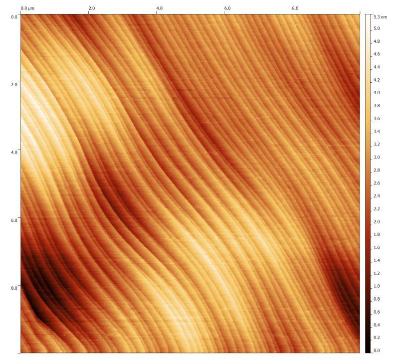
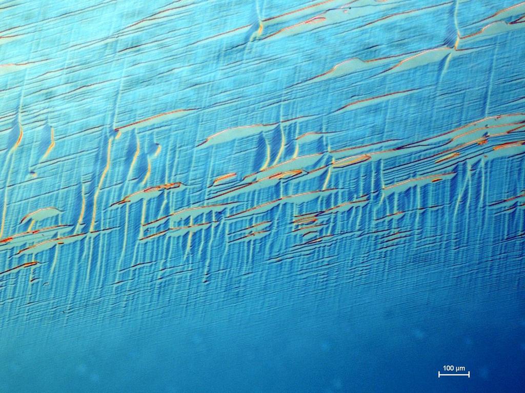
10 Atomic Force Microscope measurements H 2 - etched 6H-SiC (C-Face)
11 Planar surfaces on C-face 6H-SiC Resolved with unit-cell or ½ uc height Smoothed height profiles
 surfaces prepared under various annealing conditions: (a) 1150 C for 40 min resulting in graphene thickness of 0.")
12 Synthesis of graphene on SiC (Si-face) in vacuum FIG 3. AFM images of graphene on SiC(0001) surfaces prepared under various annealing conditions: (a) 1150 C for 40 min resulting in graphene thickness of 0.5 ML, (b) 1285 C for 40 min resulting in graphene thickness of 1.0 ML, (c) 1370 C for 40 min resulting in graphene thickness of 1.2 ML, and (d) 1390 C for 40 min resulting in graphene thickness of 1.9 ML. Images are displayed with gray scale ranges of 4, 3, 2 and 3 nm, respectively. Temperature-dependence of Epitaxial Graphene Formation on SiC(0001) Luxmi, et al. J. Electronic Materials, 38, 718 (2009) Images courtesy of Prof. Randall Feenstra, Carnegie-Mellon University, Pittsburgh, Pennsylvania.

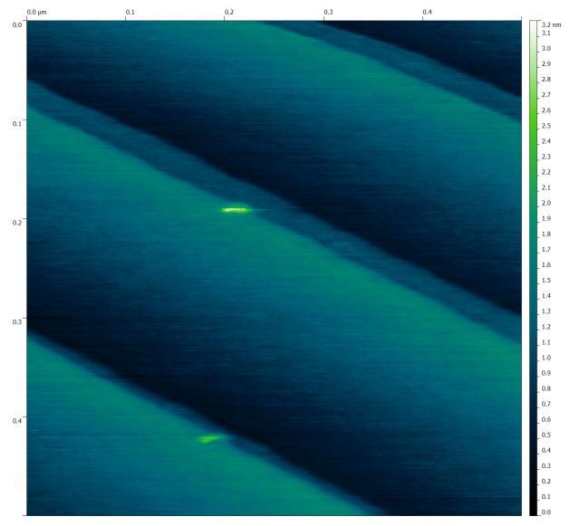
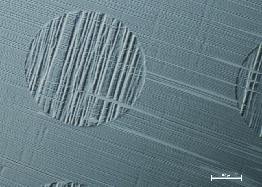
13 NIST 6H-SiC sample (Si-face) H-etched 3 min 1600 C, heated in Ar 30 min 1530 C. Auger analysis: 1.8 ML graphene Image courtesy of Prof. Randall Feenstra, Carnegie-Mellon University, Pittsburgh, Pennsylvania. AFM image, 10 m x 10 m, 8 nm gray scale (line cut gives 10 nm step bunches with spacing of about 3 m, corresponding to miscut angle of 0.2 )
14 2100 C (max) Graphite element Furnace Chamber 9 cm diameter work area Argon background gas 10 6 Torr leak checked Uniformity ± 10 C ± 90 C / minute ramp Overshoot 3 C


15 RUN 06 Samples disposition. Group 1 All graphite disks had trenches that avoid samples movement during insertion in furnace. The top graphite disk in Group 1 had its polished face towards the samples. 1 Group 2 Samples FA5 and FA3 were previously processed and reused Samples A01-H6-06 and A01-H9-06 had mesas on them

16 Epitaxial Graphene growth accompanied by etching: NIST A01-20-SE-06

17 Epitaxial Graphene growth accompanied by etching: NIST A01-20-SE-06
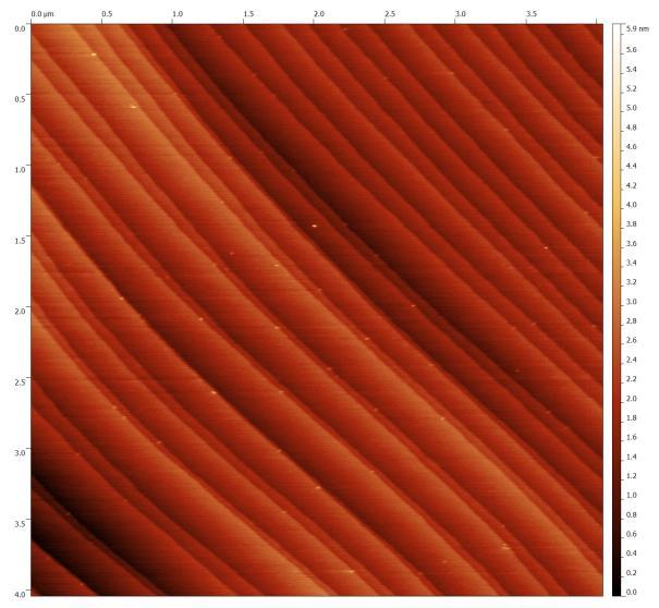
18

19 Mesa processing of polished SiC samples SF 6 Deep reactive-ion etching: 6H SiC sample (SiO2 oxidized + Ni masked)

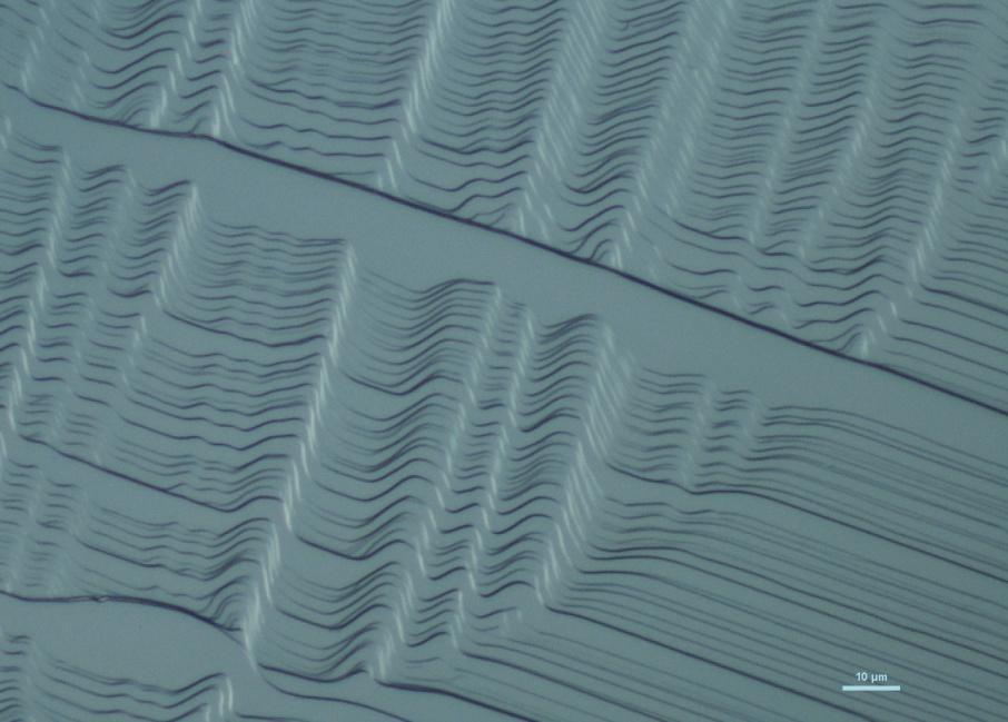
20 Atomic terraces on Mesa-etched samples
21 Graphene grown on atomic terraces: Mesa samples
 and A01-10-S-06")
22 A01-H6-06 (left, originally with mesas) and A01-10-S-06 (right)

23 A01-10-S-06, etched imprint
24 Epitaxial Graphene on SiC Terraces NIST A01-20-SE-06 by Atomic-Force Microscopy

25 G ~1611 cm -1 G ~2760 cm -1 Raman Spectra of NIST graphene on SiC Graphene cm -1
 of")
26 Epitaxial Graphene on NIST 6H SiC sample, SEM image: Raised pleats (folds) of graphene

27 Epitaxial Graphene growth at 2000 C: NIST A01-06-S-08

28 Epitaxial Graphene on SiC Terraces NIST A01-10-N-06 by Atomic-Force Microscopy Height data

29 Epitaxial Graphene on SiC Terraces NIST A01-10-N-06 by Atomic-Force Microscopy Phase data

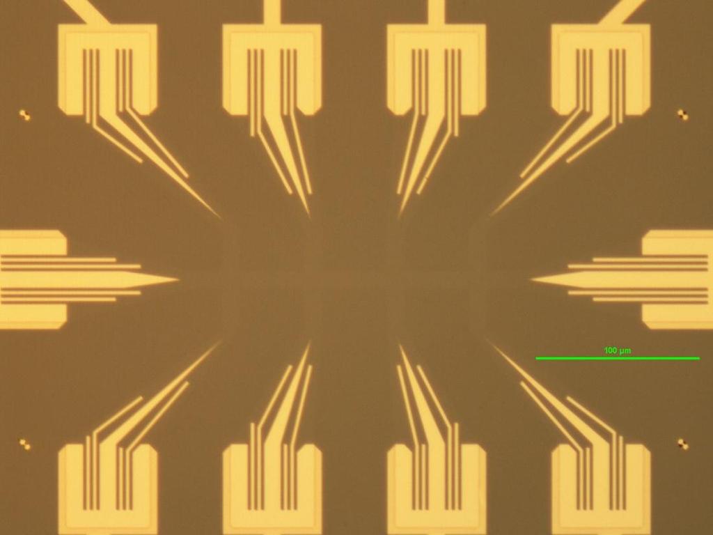

30 Graphene QHR Device fabrication
31 Epitaxial Graphene on SiC: Photochemical Gating ZEP 520A PMMA Graphene on SiC Photo-sensitive chemical layer for passivation and charge modulation
32 QHR Device characterization GaAs QHR device HH143e (1.40 K)
33 Co-authors and Contributors: Dr. Felipe L. Hernandez-Marquez (Centro Nacional de Metrologia, Mexico), Dr. Tian Shen (NIST), Dr. David B. Newell (NIST), Dr. George R. Jones (NIST), and Mr. Mariano A. Real (Instuto Nacional de Technologia Industrial, Argentina) NIST Quantum Conductance project. Dr. Irene G. Calizo and Dr. Angela R. Hight-Walker, NIST Optical Technology Division, for providing Raman Measurements and interpretation; Dr. Qingkai Yu, Center for Advanced Materials and ECE, University of Houston, who provided CVD graphene samples; Prof. Randall Feenstra, Carnegie-Mellon University, who provided SiC processing and LEEM results; Thank You
Graphene. Tianyu Ye November 30th, 2011
 Graphene Tianyu Ye November 30th, 2011 Outline What is graphene? How to make graphene? (Exfoliation, Epitaxial, CVD) Is it graphene? (Identification methods) Transport properties; Other properties; Applications;
A. Optimizing the growth conditions of large-scale graphene films
 1 A. Optimizing the growth conditions of large-scale graphene films Figure S1. Optical microscope images of graphene films transferred on 300 nm SiO 2 /Si substrates. a, Images of the graphene films grown
GRAPHENE ON THE Si-FACE OF SILICON CARBIDE USER MANUAL
 GRAPHENE ON THE Si-FACE OF SILICON CARBIDE USER MANUAL 1. INTRODUCTION Silicon Carbide (SiC) is a wide band gap semiconductor that exists in different polytypes. The substrate used for the fabrication
Graphene films on silicon carbide (SiC) wafers supplied by Nitride Crystals, Inc.
 wafers supplied by Nitride Crystals, Inc.") 9702 Gayton Road, Suite 320, Richmond, VA 23238, USA Phone: +1 (804) 709-6696 info@nitride-crystals.com www.nitride-crystals.com Graphene films on silicon carbide (SiC) wafers supplied by Nitride Crystals,
9702 Gayton Road, Suite 320, Richmond, VA 23238, USA Phone: +1 (804) 709-6696 info@nitride-crystals.com www.nitride-crystals.com Graphene films on silicon carbide (SiC) wafers supplied by Nitride Crystals,
SiC Graphene Suitable For Quantum Hall Resistance Metrology.
 SiC Graphene Suitable For Quantum Hall Resistance Metrology. Samuel Lara-Avila 1, Alexei Kalaboukhov 1, Sara Paolillo, Mikael Syväjärvi 3, Rositza Yakimova 3, Vladimir Fal'ko 4, Alexander Tzalenchuk 5,
Optimizing Graphene Morphology on SiC(0001)
") Optimizing Graphene Morphology on SiC(0001) James B. Hannon Rudolf M. Tromp Graphene sheets Graphene sheets can be formed into 0D,1D, 2D, and 3D structures Chemically inert Intrinsically high carrier mobility
Optimizing Graphene Morphology on SiC(0001) James B. Hannon Rudolf M. Tromp Graphene sheets Graphene sheets can be formed into 0D,1D, 2D, and 3D structures Chemically inert Intrinsically high carrier mobility
Supplementary Figure S1. AFM images of GraNRs grown with standard growth process. Each of these pictures show GraNRs prepared independently,
 Supplementary Figure S1. AFM images of GraNRs grown with standard growth process. Each of these pictures show GraNRs prepared independently, suggesting that the results is reproducible. Supplementary Figure
Overview. Carbon in all its forms. Background & Discovery Fabrication. Important properties. Summary & References. Overview of current research
 Graphene Prepared for Solid State Physics II Pr Dagotto Spring 2009 Laurene Tetard 03/23/09 Overview Carbon in all its forms Background & Discovery Fabrication Important properties Overview of current
Wafer-scale fabrication of graphene
 Wafer-scale fabrication of graphene Sten Vollebregt, MSc Delft University of Technology, Delft Institute of Mircosystems and Nanotechnology Delft University of Technology Challenge the future Delft University
Intrinsic Electronic Transport Properties of High. Information
 Intrinsic Electronic Transport Properties of High Quality and MoS 2 : Supporting Information Britton W. H. Baugher, Hugh O. H. Churchill, Yafang Yang, and Pablo Jarillo-Herrero Department of Physics, Massachusetts
Graphene Formation on the Carbon face of Silicon Carbide
 Carnegie Mellon University Research Showcase @ CMU Dissertations Theses and Dissertations Summer 9-2014 Graphene Formation on the Carbon face of Silicon Carbide Guowei He Carnegie Mellon University Follow
GRAPHENE the first 2D crystal lattice
 GRAPHENE the first 2D crystal lattice dimensionality of carbon diamond, graphite GRAPHENE realized in 2004 (Novoselov, Science 306, 2004) carbon nanotubes fullerenes, buckyballs what s so special about
Chapter 2 Synthesis, Structure, and Properties of Graphene and Graphene Oxide
 Chapter 2 Synthesis, Structure, and Properties of Graphene and Graphene Oxide 2.1 Introduction To develop large-area graphene-based TCFs, one of the foremost challenges is to produce sufficient amounts
1. Nanotechnology & nanomaterials -- Functional nanomaterials enabled by nanotechnologies.
 Novel Nano-Engineered Semiconductors for Possible Photon Sources and Detectors NAI-CHANG YEH Department of Physics, California Institute of Technology 1. Nanotechnology & nanomaterials -- Functional nanomaterials
A new method of growing graphene on Cu by hydrogen etching
 A new method of growing graphene on Cu by hydrogen etching Linjie zhan version 6, 2015.05.12--2015.05.24 CVD graphene Hydrogen etching Anisotropic Copper-catalyzed Highly anisotropic hydrogen etching method
Supporting Information Available:
 Supporting Information Available: Photoresponsive and Gas Sensing Field-Effect Transistors based on Multilayer WS 2 Nanoflakes Nengjie Huo 1, Shengxue Yang 1, Zhongming Wei 2, Shu-Shen Li 1, Jian-Bai Xia
SUPPLEMENTARY INFORMATION
 SUPPLEMENTARY INFORMATION Towards wafer-size graphene layers by atmospheric pressure graphitization of silicon carbide Supporting online material Konstantin V. Emtsev 1, Aaron Bostwick 2, Karsten Horn
Yugang Sun Center for Nanoscale Materials, Argonne National Laboratory, Argonne, IL 60439
 Morphology of Graphene on SiC( 000 1 ) Surfaces Luxmi, P. J. Fisher, N. Srivastava, and R. M. Feenstra Dept. Physics, Carnegie Mellon University, Pittsburgh, PA 15213 Yugang Sun Center for Nanoscale Materials,
A BIT OF MATERIALS SCIENCE THEN PHYSICS
 GRAPHENE AND OTHER D ATOMIC CRYSTALS Andre Geim with many thanks to K. Novoselov, S. Morozov, D. Jiang, F. Schedin, I. Grigorieva, J. Meyer, M. Katsnelson A BIT OF MATERIALS SCIENCE THEN PHYSICS CARBON
SUPPLEMENTARY INFORMATION
 SUPPLEMENTARY INFORMATION Facile Synthesis of High Quality Graphene Nanoribbons Liying Jiao, Xinran Wang, Georgi Diankov, Hailiang Wang & Hongjie Dai* Supplementary Information 1. Photograph of graphene
Analysis of the Formation Conditions for Large Area Epitaxial Graphene on SiC Substrates
 Analysis of the Formation Conditions for Large Area Epitaxial Graphene on SiC Substrates Rositsa Yakimova, Chariya Virojanadara, Daniela Gogova, Mikael Syväjärvi, D. Siche, Krister Larsson and Leif Johansson
Graphene FETs EE439 FINAL PROJECT. Yiwen Meng Su Ai
 Graphene FETs EE439 FINAL PROJECT Yiwen Meng Su Ai Introduction What is Graphene? An atomic-scale honeycomb lattice made of carbon atoms Before 2004, Hypothetical Carbon Structure Until 2004, physicists
Fabrication and Study of Large Area QHE Devices Based on Epitaxial Graphene.
 Fabrication and Study of Large Area QHE Devices Based on Epitaxial Graphene. S. Novikov 1, N. Lebedeva 1, K. Pierz and A. Satrapinski 3 1 Department of Micro and Nanosciences, Aalto University, Micronova,
XPS Depth Profiling of Epitaxial Graphene Intercalated with FeCl 3
 XPS Depth Profiling of Epitaxial Graphene Intercalated with FeCl 3 Mahdi Ibrahim Maynard H. Jackson High School Atlanta, GA. Faculty Advisor: Dr. Kristin Shepperd Research Group: Prof. Edward Conrad School
Supplementary Materials for
 advances.sciencemag.org/cgi/content/full/3/10/e1701661/dc1 Supplementary Materials for Defect passivation of transition metal dichalcogenides via a charge transfer van der Waals interface Jun Hong Park,
Electrical Standards based on quantum effects: Part II. Beat Jeckelmann
 Electrical Standards based on quantum effects: Part II Beat Jeckelmann Part II: The Quantum Hall Effect Overview Classical Hall effect Two-dimensional electron gas Landau levels Measurement technique Accuracy
Transient Photocurrent Measurements of Graphene Related Materials
 Transient Photocurrent Measurements of Graphene Related Materials P. Srinivasa Rao Mentor: Prof. dr. Gvido Bratina Laboratory of Organic Matter Physics University of Nova Gorica 1 Contents: 1. Electrical
Surface atoms/molecules of a material act as an interface to its surrounding environment;
 1 Chapter 1 Thesis Overview Surface atoms/molecules of a material act as an interface to its surrounding environment; their properties are often complicated by external adsorbates/species on the surface
Supporting Online Material for
 www.sciencemag.org/cgi/content/full/327/5966/662/dc Supporting Online Material for 00-GHz Transistors from Wafer-Scale Epitaxial Graphene Y.-M. Lin,* C. Dimitrakopoulos, K. A. Jenkins, D. B. Farmer, H.-Y.
Supplementary Information
 Electronic Supplementary Material (ESI) for Physical Chemistry Chemical Physics. This journal is the Owner Societies 2015 Supplementary Information Vertical Heterostructures of MoS2 and Graphene Nanoribbons
Supplementary material for High responsivity mid-infrared graphene detectors with antenna-enhanced photo-carrier generation and collection
 Supplementary material for High responsivity mid-infrared graphene detectors with antenna-enhanced photo-carrier generation and collection Yu Yao 1, Raji Shankar 1, Patrick Rauter 1, Yi Song 2, Jing Kong
Supplementary Information. Rapid Stencil Mask Fabrication Enabled One-Step. Polymer-Free Graphene Patterning and Direct
 Supplementary Information Rapid Stencil Mask Fabrication Enabled One-Step Polymer-Free Graphene Patterning and Direct Transfer for Flexible Graphene Devices Keong Yong 1,, Ali Ashraf 1,, Pilgyu Kang 1,
Supplementary Figure S1. AFM characterizations and topographical defects of h- BN films on silica substrates. (a) (c) show the AFM height
 (c) show the AFM height") Supplementary Figure S1. AFM characterizations and topographical defects of h- BN films on silica substrates. (a) (c) show the AFM height topographies of h-bn film in a size of ~1.5µm 1.5µm, 30µm 30µm
Supplementary Figure S1. AFM characterizations and topographical defects of h- BN films on silica substrates. (a) (c) show the AFM height topographies of h-bn film in a size of ~1.5µm 1.5µm, 30µm 30µm
C. D. Lee and R. M. Feenstra Dept. Physics, Carnegie Mellon University, Pittsburgh, PA 15213
 Morphology and surface reconstructions of GaN(1 1 00) surfaces C. D. Lee and R. M. Feenstra Dept. Physics, Carnegie Mellon University, Pittsburgh, PA 15213 J. E. Northrup Palo Alto Research Center, 3333
TRANSVERSE SPIN TRANSPORT IN GRAPHENE
 International Journal of Modern Physics B Vol. 23, Nos. 12 & 13 (2009) 2641 2646 World Scientific Publishing Company TRANSVERSE SPIN TRANSPORT IN GRAPHENE TARIQ M. G. MOHIUDDIN, A. A. ZHUKOV, D. C. ELIAS,
Supplementary Figures
 Supplementary Figures 1500 Heating Annealing Growing Cooling 20 Temperature ( o C) 1000 500 Ar:H 2 = 5:1 Ar:H 2 = 5:1 15 10 5 Pressure(Pa) 0 Ar(SiH 4 (5%)):C 2 H 2 = 1:2 120 mins 5 mins 5 40 mins ~120
Supporting Information
 Electronic Supplementary Material (ESI) for ChemComm. This journal is The Royal Society of Chemistry 2014 Supporting Information Controllable Atmospheric Pressure Growth of Mono-layer, Bi-layer and Tri-layer
Fabrication Technology, Part I
 EEL5225: Principles of MEMS Transducers (Fall 2004) Fabrication Technology, Part I Agenda: Microfabrication Overview Basic semiconductor devices Materials Key processes Oxidation Thin-film Deposition Reading:
Layer-modulated synthesis of uniform tungsten disulfide nanosheet using gas-phase precursors.
 Layer-modulated synthesis of uniform tungsten disulfide nanosheet using gas-phase precursors. Jusang Park * Hyungjun Kim School of Electrical and Electronics Engineering, Yonsei University, 262 Seongsanno,
Growth of Embedded and Protrusive Striped Graphene on 6H-SiC (0001)
") Growth of Embedded and Protrusive Striped Graphene on 6H-SiC (0001) A. Ruammaitree, H. Nakahara, K. Soda, Y. Saito Department of Quantum Engineering, Faculty of Engineering, Nagoya University, Nagoya 464-8603
Growth of Embedded and Protrusive Striped Graphene on 6H-SiC (0001) A. Ruammaitree, H. Nakahara, K. Soda, Y. Saito Department of Quantum Engineering, Faculty of Engineering, Nagoya University, Nagoya 464-8603
Initial Stages of Growth of Organic Semiconductors on Graphene
 Initial Stages of Growth of Organic Semiconductors on Graphene Presented by: Manisha Chhikara Supervisor: Prof. Dr. Gvido Bratina University of Nova Gorica Outline Introduction to Graphene Fabrication
Exceptional ballistic transport in epigraphene. Walt de Heer Georgia Institute of Technology
 Exceptional ballistic transport in epigraphene Walt de Heer Georgia Institute of Technology Program Objective First formulated in 2001 and patented in 2003, our objective is to develop nanoelectronics
Growing Graphene on Semiconductors
 Growing Graphene on Semiconductors edited by Nunzio Motta Francesca Iacopi Camilla Coletti Growing Graphene on Semiconductors Growing Graphene on Semiconductors edited by Nunzio Motta Francesca Iacopi
Supplementary Information Our InGaN/GaN multiple quantum wells (MQWs) based one-dimensional (1D) grating structures
 based one-dimensional (1D) grating structures") Polarized white light from hybrid organic/iii-nitrides grating structures M. Athanasiou, R. M. Smith, S. Ghataora and T. Wang* Department of Electronic and Electrical Engineering, University of Sheffield,
Polarized white light from hybrid organic/iii-nitrides grating structures M. Athanasiou, R. M. Smith, S. Ghataora and T. Wang* Department of Electronic and Electrical Engineering, University of Sheffield,
Supplementary Information
 Supplementary Information Supplementary Figure 1. fabrication. A schematic of the experimental setup used for graphene Supplementary Figure 2. Emission spectrum of the plasma: Negative peaks indicate an
Supplementary Figure 1 Detailed illustration on the fabrication process of templatestripped
 Supplementary Figure 1 Detailed illustration on the fabrication process of templatestripped gold substrate. (a) Spin coating of hydrogen silsesquioxane (HSQ) resist onto the silicon substrate with a thickness
Graphene Novel Material for Nanoelectronics
 Graphene Novel Material for Nanoelectronics Shintaro Sato Naoki Harada Daiyu Kondo Mari Ohfuchi (Manuscript received May 12, 2009) Graphene is a flat monolayer of carbon atoms with a two-dimensional honeycomb
30-Inch Roll-Based Production of High-Quality Graphene Films for Flexible Transparent Electrodes
 30-Inch Roll-Based Production of High-Quality Graphene Films for Flexible Transparent Electrodes Sukang Bae, 1* Hyeong Keun Kim, 3* Xianfang Xu, 5 Jayakumar Balakrishnan, 5 Tian Lei, 1 Young Il Song, 6
The goal of this project is to enhance the power density and lowtemperature efficiency of solid oxide fuel cells (SOFC) manufactured by atomic layer
 manufactured by atomic layer") Stanford University Michael Shandalov1, Shriram Ramanathan2, Changhyun Ko2 and Paul McIntyre1 1Department of Materials Science and Engineering, Stanford University 2Division of Engineering and Applied
Stanford University Michael Shandalov1, Shriram Ramanathan2, Changhyun Ko2 and Paul McIntyre1 1Department of Materials Science and Engineering, Stanford University 2Division of Engineering and Applied
Supplementary information
 Supplementary information Supplementary Figure S1STM images of four GNBs and their corresponding STS spectra. a-d, STM images of four GNBs are shown in the left side. The experimental STS data with respective
Growth, Processing and In-situ Observation of Graphene
 Ph.D. Thesis Growth, Processing and In-situ Observation of Graphene Mikihiro Kato Department of Physics, Graduate School of Science Tokyo University of Science 1-3 Kagurazaka, Shinjuku-ku, Tokyo 162-8601,
Chemical Vapor Deposition Graphene Grown on Peeled- Off Epitaxial Cu(111) Foil: A Simple Approach to Improved Properties
 Foil: A Simple Approach to Improved Properties") Supplementary information Chemical Vapor Deposition Graphene Grown on Peeled- Off Epitaxial Cu(111) Foil: A Simple Approach to Improved Properties Hak Ki Yu 1,2, Kannan Balasubramanian 3, Kisoo Kim 4,
Supplementary information Chemical Vapor Deposition Graphene Grown on Peeled- Off Epitaxial Cu(111) Foil: A Simple Approach to Improved Properties Hak Ki Yu 1,2, Kannan Balasubramanian 3, Kisoo Kim 4,
Figure 1: Graphene release, transfer and stacking processes. The graphene stacking began with CVD
 Supplementary figure 1 Graphene Growth and Transfer Graphene PMMA FeCl 3 DI water Copper foil CVD growth Back side etch PMMA coating Copper etch in 0.25M FeCl 3 DI water rinse 1 st transfer DI water 1:10
Supporting Information. Fast Synthesis of High-Performance Graphene by Rapid Thermal Chemical Vapor Deposition
 1 Supporting Information Fast Synthesis of High-Performance Graphene by Rapid Thermal Chemical Vapor Deposition Jaechul Ryu, 1,2, Youngsoo Kim, 4, Dongkwan Won, 1 Nayoung Kim, 1 Jin Sung Park, 1 Eun-Kyu
Graphene The Search For Two Dimensions. Christopher Scott Friedline Arizona State University
 Graphene The Search For Two Dimensions Christopher Scott Friedline Arizona State University What Is Graphene? Single atomic layer of graphite arranged in a honeycomb crystal lattice Consists of sp 2 -bonded
CVD growth of Graphene. SPE ACCE presentation Carter Kittrell James M. Tour group September 9 to 11, 2014
 CVD growth of Graphene SPE ACCE presentation Carter Kittrell James M. Tour group September 9 to 11, 2014 Graphene zigzag armchair History 1500: Pencil-Is it made of lead? 1789: Graphite 1987: The first
Supplementary Information
 Supplementary Information Plasma-assisted reduction of graphene oxide at low temperature and atmospheric pressure for flexible conductor applications Seung Whan Lee 1, Cecilia Mattevi 2, Manish Chhowalla
A Novel Approach to the Layer Number-Controlled and Grain Size- Controlled Growth of High Quality Graphene for Nanoelectronics
 Supporting Information A Novel Approach to the Layer Number-Controlled and Grain Size- Controlled Growth of High Quality Graphene for Nanoelectronics Tej B. Limbu 1,2, Jean C. Hernández 3, Frank Mendoza
Large Scale Direct Synthesis of Graphene on Sapphire and Transfer-free Device Fabrication
 Supplementary Information Large Scale Direct Synthesis of Graphene on Sapphire and Transfer-free Device Fabrication Hyun Jae Song a, Minhyeok Son a, Chibeom Park a, Hyunseob Lim a, Mark P. Levendorf b,
Graphene Fundamentals and Emergent Applications
 Graphene Fundamentals and Emergent Applications Jamie H. Warner Department of Materials University of Oxford Oxford, UK Franziska Schaffel Department of Materials University of Oxford Oxford, UK Alicja
Lecture 3: Heterostructures, Quasielectric Fields, and Quantum Structures
 Lecture 3: Heterostructures, Quasielectric Fields, and Quantum Structures MSE 6001, Semiconductor Materials Lectures Fall 2006 3 Semiconductor Heterostructures A semiconductor crystal made out of more
Nanostructure. Materials Growth Characterization Fabrication. More see Waser, chapter 2
 Nanostructure Materials Growth Characterization Fabrication More see Waser, chapter 2 Materials growth - deposition deposition gas solid Physical Vapor Deposition Chemical Vapor Deposition Physical Vapor
NiCl2 Solution concentration. Etching Duration. Aspect ratio. Experiment Atmosphere Temperature. Length(µm) Width (nm) Ar:H2=9:1, 150Pa
 Width (nm) Ar:H2=9:1, 150Pa") Experiment Atmosphere Temperature #1 # 2 # 3 # 4 # 5 # 6 # 7 # 8 # 9 # 10 Ar:H2=9:1, 150Pa Ar:H2=9:1, 150Pa Ar:H2=9:1, 150Pa Ar:H2=9:1, 150Pa Ar:H2=9:1, 150Pa Ar:H2=9:1, 150Pa Ar:H2=9:1, 150Pa Ar:H2=9:1,
Experiment Atmosphere Temperature #1 # 2 # 3 # 4 # 5 # 6 # 7 # 8 # 9 # 10 Ar:H2=9:1, 150Pa Ar:H2=9:1, 150Pa Ar:H2=9:1, 150Pa Ar:H2=9:1, 150Pa Ar:H2=9:1, 150Pa Ar:H2=9:1, 150Pa Ar:H2=9:1, 150Pa Ar:H2=9:1,
Ferromagnetism and Anomalous Hall Effect in Graphene
 Ferromagnetism and Anomalous Hall Effect in Graphene Jing Shi Department of Physics & Astronomy, University of California, Riverside Graphene/YIG Introduction Outline Proximity induced ferromagnetism Quantized
Modulation-Doped Growth of Mosaic Graphene with Single Crystalline. p-n Junctions for Efficient Photocurrent Generation
 Modulation-Doped Growth of Mosaic Graphene with Single Crystalline p-n Junctions for Efficient Photocurrent Generation Kai Yan 1,, Di Wu 1,, Hailin Peng 1, *, Li Jin 2, Qiang Fu 2, Xinhe Bao 2 and Zhongfan
Supplementary Information for. Origin of New Broad Raman D and G Peaks in Annealed Graphene
 Supplementary Information for Origin of New Broad Raman D and G Peaks in Annealed Graphene Jinpyo Hong, Min Kyu Park, Eun Jung Lee, DaeEung Lee, Dong Seok Hwang and Sunmin Ryu* Department of Applied Chemistry,
Paper and Cellulosic Materials as Flexible Substrates for 2D Electronic Materials
 Paper and Cellulosic Materials as Flexible Substrates for 2D Electronic Materials Prof. Eric M. Vogel, Prof. M. Shofner, Brian Beatty Materials Science & Engineering Trends in Electronics Internet of things
Two-Dimensional (C 4 H 9 NH 3 ) 2 PbBr 4 Perovskite Crystals for. High-Performance Photodetector. Supporting Information for
 2 PbBr 4 Perovskite Crystals for. High-Performance Photodetector. Supporting Information for") Supporting Information for Two-Dimensional (C 4 H 9 NH 3 ) 2 PbBr 4 Perovskite Crystals for High-Performance Photodetector Zhenjun Tan,,ǁ, Yue Wu,ǁ, Hao Hong, Jianbo Yin, Jincan Zhang,, Li Lin, Mingzhan
Supporting Information for Two-Dimensional (C 4 H 9 NH 3 ) 2 PbBr 4 Perovskite Crystals for High-Performance Photodetector Zhenjun Tan,,ǁ, Yue Wu,ǁ, Hao Hong, Jianbo Yin, Jincan Zhang,, Li Lin, Mingzhan
Lecture 20: Semiconductor Structures Kittel Ch 17, p , extra material in the class notes
 Lecture 20: Semiconductor Structures Kittel Ch 17, p 494-503, 507-511 + extra material in the class notes MOS Structure Layer Structure metal Oxide insulator Semiconductor Semiconductor Large-gap Semiconductor
Frictional characteristics of exfoliated and epitaxial graphene
 Frictional characteristics of exfoliated and epitaxial graphene Young Jun Shin a,b, Ryan Stromberg c, Rick Nay c, Han Huang d, Andrew T. S. Wee d, Hyunsoo Yang a,b,*, Charanjit S. Bhatia a a Department
The Inclusion of Impurities in Graphene Grown on Silicon Carbide
 The Inclusion of Impurities in Graphene Grown on Silicon Carbide Sara Rothwell May 23, 2013 Goal: Experimentally Fabricate Doped Graphene Procedure: 1. Introduce dopant in substrate ImplantaEon NO Process
SUPPLEMENTARY INFORMATION
 Lateral heterojunctions within monolayer MoSe 2 -WSe 2 semiconductors Chunming Huang 1,#,*, Sanfeng Wu 1,#,*, Ana M. Sanchez 2,#,*, Jonathan J. P. Peters 2, Richard Beanland 2, Jason S. Ross 3, Pasqual
Nanostrukturphysik (Nanostructure Physics)
") Nanostrukturphysik (Nanostructure Physics) Prof. Yong Lei & Dr. Yang Xu Fachgebiet 3D-Nanostrukturierung, Institut für Physik Contact: yong.lei@tu-ilmenau.de; yang.xu@tu-ilmenau.de Office: Unterpoerlitzer
Nanostrukturphysik (Nanostructure Physics) Prof. Yong Lei & Dr. Yang Xu Fachgebiet 3D-Nanostrukturierung, Institut für Physik Contact: yong.lei@tu-ilmenau.de; yang.xu@tu-ilmenau.de Office: Unterpoerlitzer
SUPPLEMENTARY INFORMATION
 Direct Visualization of Large-Area Graphene Domains and Boundaries by Optical Birefringency Dae Woo Kim 1,*, Yun Ho Kim 1,2,*, Hyeon Su Jeong 1, Hee-Tae Jung 1 * These authors contributed equally to this
Crystalline Surfaces for Laser Metrology
 Crystalline Surfaces for Laser Metrology A.V. Latyshev, Institute of Semiconductor Physics SB RAS, Novosibirsk, Russia Abstract: The number of methodological recommendations has been pronounced to describe
Supplementary Figure 1: Micromechanical cleavage of graphene on oxygen plasma treated Si/SiO2. Supplementary Figure 2: Comparison of hbn yield.
 1 2 3 4 Supplementary Figure 1: Micromechanical cleavage of graphene on oxygen plasma treated Si/SiO 2. Optical microscopy images of three examples of large single layer graphene flakes cleaved on a single
Classification of Solids
 Classification of Solids Classification by conductivity, which is related to the band structure: (Filled bands are shown dark; D(E) = Density of states) Class Electron Density Density of States D(E) Examples
Carbon based Nanoscale Electronics
 Carbon based Nanoscale Electronics 09 02 200802 2008 ME class Outline driving force for the carbon nanomaterial electronic properties of fullerene exploration of electronic carbon nanotube gold rush of
Wafer Scale Homogeneous Bilayer Graphene Films by. Chemical Vapor Deposition
 Supporting Information for Wafer Scale Homogeneous Bilayer Graphene Films by Chemical Vapor Deposition Seunghyun Lee, Kyunghoon Lee, Zhaohui Zhong Department of Electrical Engineering and Computer Science,
Determining Carbon Nanotube Properties from Raman. Scattering Measurements
 Determining Carbon Nanotube Properties from Raman Scattering Measurements Ying Geng 1, David Fang 2, and Lei Sun 3 1 2 3 The Institute of Optics, Electrical and Computer Engineering, Laboratory for Laser
Selective Manipulation of Molecules by Electrostatic Force and Detection of Single Molecules in Aqueous Solution
 Supporting Information Selective Manipulation of Molecules by Electrostatic Force and Detection of Single Molecules in Aqueous Solution Zhongbo Yan, Ming Xia, Pei Zhang, and Ya-Hong Xie* Department of
Supplementary Figure 1 Experimental setup for crystal growth. Schematic drawing of the experimental setup for C 8 -BTBT crystal growth.
 Supplementary Figure 1 Experimental setup for crystal growth. Schematic drawing of the experimental setup for C 8 -BTBT crystal growth. Supplementary Figure 2 AFM study of the C 8 -BTBT crystal growth
Toward Clean Suspended CVD Graphene
 Electronic Supplementary Material (ESI) for RSC Advances. This journal is The Royal Society of Chemistry 2016 Supplemental information for Toward Clean Suspended CVD Graphene Alexander Yulaev 1,2,3, Guangjun
Physics and Material Science of Semiconductor Nanostructures
 Physics and Material Science of Semiconductor Nanostructures PHYS 570P Prof. Oana Malis Email: omalis@purdue.edu Course website: http://www.physics.purdue.edu/academic_programs/courses/phys570p/ Lecture
EE130: Integrated Circuit Devices
 EE130: Integrated Circuit Devices (online at http://webcast.berkeley.edu) Instructor: Prof. Tsu-Jae King (tking@eecs.berkeley.edu) TA s: Marie Eyoum (meyoum@eecs.berkeley.edu) Alvaro Padilla (apadilla@eecs.berkeley.edu)
Formation of Epitaxial Graphene on SiC(0001) using Vacuum or Argon Environments
 using Vacuum or Argon Environments") Formation of Epitaxial Graphene on SiC(0001) using Vacuum or Argon Environments Luxmi, N. Srivastava, and R. M. Feenstra Department of Physics, Carnegie Mellon University, Pittsburgh, PA 15213 P. J. Fisher
Formation of Epitaxial Graphene on SiC(0001) using Vacuum or Argon Environments Luxmi, N. Srivastava, and R. M. Feenstra Department of Physics, Carnegie Mellon University, Pittsburgh, PA 15213 P. J. Fisher
Lectures Graphene and
 Lectures 15-16 Graphene and carbon nanotubes Graphene is atomically thin crystal of carbon which is stronger than steel but flexible, is transparent for light, and conducts electricity (gapless semiconductor).
OPTI510R: Photonics. Khanh Kieu College of Optical Sciences, University of Arizona Meinel building R.626
 OPTI510R: Photonics Khanh Kieu College of Optical Sciences, University of Arizona kkieu@optics.arizona.edu Meinel building R.626 Announcements HW#3 is assigned due Feb. 20 st Mid-term exam Feb 27, 2PM
Interface Structure of Graphene on SiC for Various Preparation Conditions
 Interface Structure of Graphene on SiC for Various Preparation Conditions Doctoral Thesis May, 2012 Nishtha Srivastava Advisor Prof. R. M. Feenstra Dept. of Physics, Carnegie Mellon University, Pittsburgh,
Nanostrukturphysik (Nanostructure Physics)
") Nanostrukturphysik (Nanostructure Physics) Prof. Yong Lei & Dr. Yang Xu Fachgebiet 3D-Nanostrukturierung, Institut für Physik Contact: yong.lei@tu-ilmenau.de; yang.xu@tu-ilmenau.de Office: Unterpoerlitzer
Nanostrukturphysik (Nanostructure Physics) Prof. Yong Lei & Dr. Yang Xu Fachgebiet 3D-Nanostrukturierung, Institut für Physik Contact: yong.lei@tu-ilmenau.de; yang.xu@tu-ilmenau.de Office: Unterpoerlitzer
Supplementary Figures Supplementary Figure 1
 Supplementary Figures Supplementary Figure 1 Optical images of graphene grains on Cu after Cu oxidation treatment at 200 for 1m 30s. Each sample was synthesized with different H 2 annealing time for (a)
Monolayer Semiconductors
 Monolayer Semiconductors Gilbert Arias California State University San Bernardino University of Washington INT REU, 2013 Advisor: Xiaodong Xu (Dated: August 24, 2013) Abstract Silicon may be unable to
Plastic Electronics. Joaquim Puigdollers.
 Plastic Electronics Joaquim Puigdollers Joaquim.puigdollers@upc.edu Nobel Prize Chemistry 2000 Origins Technological Interest First products.. MONOCROMATIC PHILIPS Today Future Technological interest Low
Field effect in epitaxial graphene on a silicon carbide substrate
 Field effect in epitaxial graphene on a silicon carbide substrate Gong Gu a) Sarnoff Corporation, CN5300, Princeton, New Jersey 08543 Shu Nie and R. M. Feenstra Department of Physics, Carnegie Mellon University,
Energy Spectroscopy. Excitation by means of a probe
 Energy Spectroscopy Excitation by means of a probe Energy spectral analysis of the in coming particles -> XAS or Energy spectral analysis of the out coming particles Different probes are possible: Auger
Supporting Information
 Supporting Information Assembly and Densification of Nanowire Arrays via Shrinkage Jaehoon Bang, Jonghyun Choi, Fan Xia, Sun Sang Kwon, Ali Ashraf, Won Il Park, and SungWoo Nam*,, Department of Mechanical
Supplementary Information. for. Controlled Scalable Synthesis of Uniform, High-Quality Monolayer and Fewlayer
 Supplementary Information for Controlled Scalable Synthesis of Uniform, High-Quality Monolayer and Fewlayer MoS 2 Films Yifei Yu 1, Chun Li 1, Yi Liu 3, Liqin Su 4, Yong Zhang 4, Linyou Cao 1,2 * 1 Department
Epitaxial graphene on SiC
 Epitaxial graphene n SiC A rute twards high-perfrmance electrnic devices Albert García Outline 1. GPNT: a brief intrductin 2. Graphene n SiC 3. Back-gated graphene 4. Cnclusins Outline 1. GPNT: a brief
Investigation of graphene layer application to RF-grade copper surfaces
 Investigation of graphene layer application to RF-grade copper surfaces Alex Murokh RadiaBeam Technologies, LLC. SLAC National Accelerator Laboratory, February 10, 2011 Motivation High gradient research
Plasma Deposition (Overview) Lecture 1
 Lecture 1") Plasma Deposition (Overview) Lecture 1 Material Processes Plasma Processing Plasma-assisted Deposition Implantation Surface Modification Development of Plasma-based processing Microelectronics needs (fabrication
Plasma Deposition (Overview) Lecture 1 Material Processes Plasma Processing Plasma-assisted Deposition Implantation Surface Modification Development of Plasma-based processing Microelectronics needs (fabrication