Lectures Graphene and
|
|
|
- Stanley Johns
- 6 years ago
- Views:
Transcription


1 Lectures Graphene and carbon nanotubes Graphene is atomically thin crystal of carbon which is stronger than steel but flexible, is transparent for light, and conducts electricity (gapless semiconductor).


2 D.I.Y. Graphene Geim & Novoselov (Manchester) 004
3 Graphene from a nanopensil Kim (Columbia Univ) 005


 Geim & Novoselov")
 Geim & MacDonald,")
 Geim & Kim,")
4 Ultra-thin graphitic films mechanically exfoliated from bulk graphite Novoselov & Geim (Manchester) Science 306, 666 (004) Geim & Novoselov - Nature Materials 6, 183 (007) Geim & MacDonald, Physics Today 60, (007) Geim & Kim, Scientific American (April 008) 10 nm
5 Carbon has 4 electrons in the outer s-p shell sp hybridisation forms strong directed bonds which determine a honeycomb lattice structure. - bonds C sp Strong hybridised bonds make graphene mechanically strong. It takes 48,000 kn m kg 1 (compare to best steel's 154 kn m kg 1 ). Also, it is chemically resilient. strong covalent bonds * empty?- conduction properties full

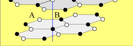
6 hexagonal Bravais lattice R n 1 n n1a1 na unit cell can be chosen differently full sites 6x1/3sites


7 Carbon has 4 electrons in the outer s-p shell sp hybridisation forms strong directed bonds which determine a honeycomb lattice structure. * p z - bonds ( ) C 0 ~ 3eV orbitals determine conduction properties of graphite p z -bands ~ 10eV
8 Bragg scattering conditions G R Reciprocal lattice G N N1 G1 N G 1 N a1 G 1 a 1 ; G 1 S a G a ; G ig R 1n e n 1 n n M 1 1 G G G unitcell S unitcell G 1 Hexagonal Bravais lattice determines a hexagonal reciprocal lattice, with G 1 G a a 4 3 / 3a
9 Reciprocal lattice ( k G ) ( k ) ( N k 1N G G N N N1 G1 N G 1 G Hexagonal reciprocal lattice corresponding to the hexagonal Bravais lattice 1 st Brilloun zone G 1

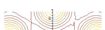
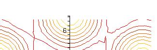
 E F")
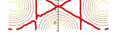
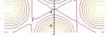
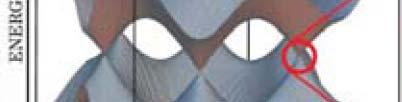
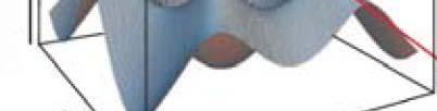
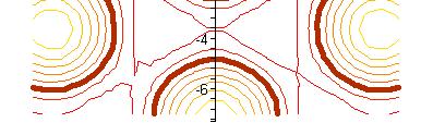
10 Fermi point in graphene ( k ) E F
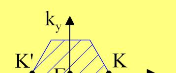
11 G Valley G '

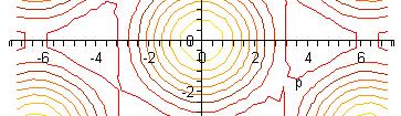
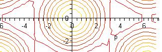
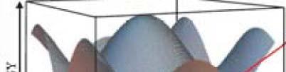
12 Graphene (monolayer of graphite) is an atomically thin zero-gap two-dimensional semiconductor with linear dispersion of conduction and valence band electrons. cond vp v p x py p y p x Electronic dispersion in the vicinity of the corner of the Brillouin zone: the same in both valleys. val vp v p x p y


 of heavily doped graphene synthesized on silicon")
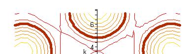
13 Simultaneous detection high-energy photon of the energy, E and ħω~ ev propagation angle θ of photo-electrons enables me cos one to restore ( p ) A E completely the band structure. p work function Angle-resolved photo-emission spectroscopy (ARPES) of heavily doped graphene synthesized on silicon carbide A. Bostwick et al Nature Physics, 3, 36 (007)

 hl")


14 Graphene: gapless semiconductor DoS Wallace, Phys. Rev. 71, 6 (1947) hl holes electrons ncarriers V gate Graphene-based field-effect transistor: GraFET Geim and Novoselov, Nature Mat. 6, 183 (007)


, et al Nano")
15 Graphene-based pixels graphene When embedded in polymers, graphene reinforces them, remains conducting and, since it s thin, it is highly transparent. Thus, it is an ideal material to make flexible liquid crystal screens Blake (Graphene Industries Ltd), et al Nano Lett. 8, 1704, (008) or to be used in conducting coating.


16 Graphene: state of the art in applicaitons G sublimated on inch-size SiC is used G grown on copper and transferred into various media G exfoliated from bulk graphite into for manufacturing THz circuits. IBM & HRL (USA) is used for flexible optoelectronics, suspensions is used to enhance mechanical LCD displays, touch screens. properties of light-weight (Samsung) materials (for aerospace and medical implants ).


17


18 Carbon nanotubes Iijima 1991 Smalley 1993 STM images of carbon nanotubes T.W. Odom, J.-L. Huang, P.Kim, C.Lieber, Nature 391 (1998)

19 Nanotubes growth

")

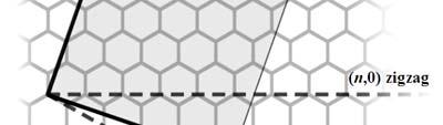
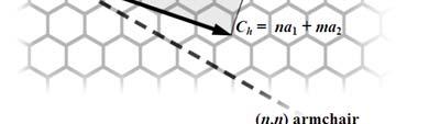


20 Nanotube types armchair (n,n) metallic zig-zag (n,0) semiconductor chiral (n,m) with n-m=3 small-gap semiconductors

21 ( y 0) ( y L ) Metallic nanotubes (n,n) ~ p y 1 L e L i y / L M perimeter, πr cond v p x p y n 1 cond n v p x h M L p y p x F n 0 p x n 0,1,,3,... M val val v px p n v px y L h M


22 M 1 Metallic nanotubes (m,m ) with m=m truly 1D conductors density of states v p x M 0 p x M 11 M 1 1 DoS v M 0 Yao et al (TUDelft)1999


23 Semicondutor-type nanotubes (different n and m) Depending on how the carbon sheet is rolled into a nanotube, the resulting nanotube may have a gap in the electron spectrum. A gap in the nanotube spectrum is determined by its radius r,, which offers a direct root towards engineering semiconductor wires with a prescribed band gap, for use in electronic and optoelectronic devices. gap v r p x tunnelling current T.W. Odom, J.-L. Huang, P. Kim, C. Lieber, Nature 391 (1998)

.")
24 Potential applications of carbon nanotubes: In surface tunnelling microscopy used as a tip. Make excellent tips for field-effect electron guns for plasma. displays (SONY). equi-potential t lines

 of fundamental properties of new")

25 Northwest Doctoral Training Centre in Nanoscience Initial training designed to demonstrate the breadth and potential of nanoscience, before focusing on one specific area of the subject. Research and training in fundamental nanoscience, practical nano-engineering, and nanotechnology in medicine. Interdisciplinary PhD projects which span from development and studies (exp and th) of fundamental properties of new materials and structures to making devices for applications in electronics and medicine. Development of skills in nanofabrication, low-temperature physics, materials science and data storage, synthetic chemistry, cell &tissue biology, biophysics, nanophotonics and materials science this will be your choice!
The many forms of carbon
 The many forms of carbon Carbon is not only the basis of life, it also provides an enormous variety of structures for nanotechnology. This versatility is connected to the ability of carbon to form two
Graphene films on silicon carbide (SiC) wafers supplied by Nitride Crystals, Inc.
 wafers supplied by Nitride Crystals, Inc.") 9702 Gayton Road, Suite 320, Richmond, VA 23238, USA Phone: +1 (804) 709-6696 info@nitride-crystals.com www.nitride-crystals.com Graphene films on silicon carbide (SiC) wafers supplied by Nitride Crystals,
9702 Gayton Road, Suite 320, Richmond, VA 23238, USA Phone: +1 (804) 709-6696 info@nitride-crystals.com www.nitride-crystals.com Graphene films on silicon carbide (SiC) wafers supplied by Nitride Crystals,
3-month progress Report
 3-month progress Report Graphene Devices and Circuits Supervisor Dr. P.A Childs Table of Content Abstract... 1 1. Introduction... 1 1.1 Graphene gold rush... 1 1.2 Properties of graphene... 3 1.3 Semiconductor
Graphene and Carbon Nanotubes
 Graphene and Carbon Nanotubes 1 atom thick films of graphite atomic chicken wire Novoselov et al - Science 306, 666 (004) 100μm Geim s group at Manchester Novoselov et al - Nature 438, 197 (005) Kim-Stormer
ELECTRONIC ENERGY DISPERSION AND STRUCTURAL PROPERTIES ON GRAPHENE AND CARBON NANOTUBES
 ELECTRONIC ENERGY DISPERSION AND STRUCTURAL PROPERTIES ON GRAPHENE AND CARBON NANOTUBES D. RACOLTA, C. ANDRONACHE, D. TODORAN, R. TODORAN Technical University of Cluj Napoca, North University Center of
From Graphene to Nanotubes
 From Graphene to Nanotubes Zone Folding and Quantum Confinement at the Example of the Electronic Band Structure Christian Krumnow christian.krumnow@fu-berlin.de Freie Universität Berlin June 6, Zone folding
Carbon nanotubes and Graphene
 16 October, 2008 Solid State Physics Seminar Main points 1 History and discovery of Graphene and Carbon nanotubes 2 Tight-binding approximation Dynamics of electrons near the Dirac-points 3 Properties
SiC Graphene Suitable For Quantum Hall Resistance Metrology.
 SiC Graphene Suitable For Quantum Hall Resistance Metrology. Samuel Lara-Avila 1, Alexei Kalaboukhov 1, Sara Paolillo, Mikael Syväjärvi 3, Rositza Yakimova 3, Vladimir Fal'ko 4, Alexander Tzalenchuk 5,
Graphene Novel Material for Nanoelectronics
 Graphene Novel Material for Nanoelectronics Shintaro Sato Naoki Harada Daiyu Kondo Mari Ohfuchi (Manuscript received May 12, 2009) Graphene is a flat monolayer of carbon atoms with a two-dimensional honeycomb
Calculating Electronic Structure of Different Carbon Nanotubes and its Affect on Band Gap
 Calculating Electronic Structure of Different Carbon Nanotubes and its Affect on Band Gap 1 Rashid Nizam, 2 S. Mahdi A. Rizvi, 3 Ameer Azam 1 Centre of Excellence in Material Science, Applied Physics AMU,
1. Nanotechnology & nanomaterials -- Functional nanomaterials enabled by nanotechnologies.
 Novel Nano-Engineered Semiconductors for Possible Photon Sources and Detectors NAI-CHANG YEH Department of Physics, California Institute of Technology 1. Nanotechnology & nanomaterials -- Functional nanomaterials
Transparent Electrode Applications
 Transparent Electrode Applications LCD Solar Cells Touch Screen Indium Tin Oxide (ITO) Zinc Oxide (ZnO) - High conductivity - High transparency - Resistant to environmental effects - Rare material (Indium)
PH575 Spring Lecture #28 Nanoscience: the case study of graphene and carbon nanotubes.
 PH575 Spring 2014 Lecture #28 Nanoscience: the case study of graphene and carbon nanotubes. Nanoscience scale 1-100 nm "Artificial atoms" Small size => discrete states Large surface to volume ratio Bottom-up
Monolayer Semiconductors
 Monolayer Semiconductors Gilbert Arias California State University San Bernardino University of Washington INT REU, 2013 Advisor: Xiaodong Xu (Dated: August 24, 2013) Abstract Silicon may be unable to
Graphite, graphene and relativistic electrons
 Graphite, graphene and relativistic electrons Introduction Physics of E. graphene Y. Andrei Experiments Rutgers University Transport electric field effect Quantum Hall Effect chiral fermions STM Dirac
So why is sodium a metal? Tungsten Half-filled 5d band & half-filled 6s band. Insulators. Interaction of metals with light?
 Bonding in Solids: Metals, Insulators, & CHEM 107 T. Hughbanks Delocalized bonding in Solids Think of a pure solid as a single, very large molecule. Use our bonding pictures to try to understand properties.
Nanoscience quantum transport
 Nanoscience quantum transport Janine Splettstößer Applied Quantum Physics, MC2, Chalmers University of Technology Chalmers, November 2 10 Plan/Outline 4 Lectures (1) Introduction to quantum transport (2)
Graphene A One-Atom-Thick Material for Microwave Devices
 ROMANIAN JOURNAL OF INFORMATION SCIENCE AND TECHNOLOGY Volume 11, Number 1, 2008, 29 35 Graphene A One-Atom-Thick Material for Microwave Devices D. DRAGOMAN 1, M. DRAGOMAN 2, A. A. MÜLLER3 1 University
Lecture 3: Electron statistics in a solid
 Lecture 3: Electron statistics in a solid Contents Density of states. DOS in a 3D uniform solid.................... 3.2 DOS for a 2D solid........................ 4.3 DOS for a D solid........................
Graphene: the Route from Touch Screens to Digital Nanoelectronics
 Graphene: the Route from Touch Screens to Digital Nanoelectronics László Péter Biró Research Institute for Technical Physics & Materials Science, Budapest, Hungary http://www.nanotechnology.hu/ Human History
Seminars in Nanosystems - I
 Seminars in Nanosystems - I Winter Semester 2011/2012 Dr. Emanuela Margapoti Emanuela.Margapoti@wsi.tum.de Dr. Gregor Koblmüller Gregor.Koblmueller@wsi.tum.de Seminar Room at ZNN 1 floor Topics of the
Electron Interactions and Nanotube Fluorescence Spectroscopy C.L. Kane & E.J. Mele
 Electron Interactions and Nanotube Fluorescence Spectroscopy C.L. Kane & E.J. Mele Large radius theory of optical transitions in semiconducting nanotubes derived from low energy theory of graphene Phys.
Electronic properties of graphene. Jean-Noël Fuchs Laboratoire de Physique des Solides Université Paris-Sud (Orsay)
") Electronic properties of graphene Jean-Noël Fuchs Laboratoire de Physique des Solides Université Paris-Sud (Orsay) Cargèse, September 2012 3 one-hour lectures in 2 x 1,5h on electronic properties of graphene
Electronic properties of graphene Jean-Noël Fuchs Laboratoire de Physique des Solides Université Paris-Sud (Orsay) Cargèse, September 2012 3 one-hour lectures in 2 x 1,5h on electronic properties of graphene
Calculation of Cutting Lines of Single-Walled Carbon Nanotubes
 65 C.Ü. Fen Fakültesi Fen Bilimleri Dergisi, Cilt 33, No. 1 (2012) Calculation of Cutting Lines of Single-Walled Carbon Nanotubes Erdem UZUN 1* 1 Karamanoğlu Mehmetbey Üniversitesi, Fen Fakültesi, Fizik
Overview. Carbon in all its forms. Background & Discovery Fabrication. Important properties. Summary & References. Overview of current research
 Graphene Prepared for Solid State Physics II Pr Dagotto Spring 2009 Laurene Tetard 03/23/09 Overview Carbon in all its forms Background & Discovery Fabrication Important properties Overview of current
2 Symmetry. 2.1 Structure of carbon nanotubes
 2 Symmetry Carbon nanotubes are hollow cylinders of graphite sheets. They can be viewed as single molecules, regarding their small size ( nm in diameter and µm length), or as quasi-one dimensional crystals
PHYS 3313 Section 001 Lecture #21 Monday, Nov. 26, 2012
 PHYS 3313 Section 001 Lecture #21 Monday, Nov. 26, 2012 Superconductivity Theory, The Cooper Pair Application of Superconductivity Semi-Conductor Nano-technology Graphene 1 Announcements Your presentations
structure of graphene and carbon nanotubes which forms the basis for many of their proposed applications in electronics.
 Chapter Basics of graphene and carbon nanotubes This chapter reviews the theoretical understanding of the geometrical and electronic structure of graphene and carbon nanotubes which forms the basis for
Solid State Device Fundamentals
 Solid State Device Fundamentals ENS 345 Lecture Course by Alexander M. Zaitsev alexander.zaitsev@csi.cuny.edu Tel: 718 982 2812 Office 4N101b 1 The free electron model of metals The free electron model
ESE370: Circuit-Level Modeling, Design, and Optimization for Digital Systems
 ESE370: Circuit-Level Modeling, Design, and Optimization for Digital Systems Lec 6: September 14, 2015 MOS Model You are Here: Transistor Edition! Previously: simple models (0 and 1 st order) " Comfortable
Nanostructures. Lecture 13 OUTLINE
 Nanostructures MTX9100 Nanomaterials Lecture 13 OUTLINE -What is quantum confinement? - How can zero-dimensional materials be used? -What are one dimensional structures? -Why does graphene attract so much
Graphene. Tianyu Ye November 30th, 2011
 Graphene Tianyu Ye November 30th, 2011 Outline What is graphene? How to make graphene? (Exfoliation, Epitaxial, CVD) Is it graphene? (Identification methods) Transport properties; Other properties; Applications;
Optimizing Graphene Morphology on SiC(0001)
") Optimizing Graphene Morphology on SiC(0001) James B. Hannon Rudolf M. Tromp Graphene sheets Graphene sheets can be formed into 0D,1D, 2D, and 3D structures Chemically inert Intrinsically high carrier mobility
Optimizing Graphene Morphology on SiC(0001) James B. Hannon Rudolf M. Tromp Graphene sheets Graphene sheets can be formed into 0D,1D, 2D, and 3D structures Chemically inert Intrinsically high carrier mobility
& Dirac Fermion confinement Zahra Khatibi
 Graphene & Dirac Fermion confinement Zahra Khatibi 1 Outline: What is so special about Graphene? applications What is Graphene? Structure Transport properties Dirac fermions confinement Necessity External
Nanotechnology in Consumer Products
 Nanotechnology in Consumer Products June 17, 2015 October 31, 2014 The webinar will begin at 1pm Eastern Time Perform an audio check by going to Tools > Audio > Audio Setup Wizard Chat Box Chat Box Send
ESE370: Circuit-Level Modeling, Design, and Optimization for Digital Systems
 ESE370: Circuit-Level Modeling, Design, and Optimization for Digital Systems Lec 6: September 18, 2017 MOS Model You are Here: Transistor Edition! Previously: simple models (0 and 1 st order) " Comfortable
First-Hand Investigation: Modeling of Semiconductors
 perform an investigation to model the behaviour of semiconductors, including the creation of a hole or positive charge on the atom that has lost the electron and the movement of electrons and holes in
Quantum Oscillations in Graphene in the Presence of Disorder
 WDS'9 Proceedings of Contributed Papers, Part III, 97, 9. ISBN 978-8-778-- MATFYZPRESS Quantum Oscillations in Graphene in the Presence of Disorder D. Iablonskyi Taras Shevchenko National University of
Nanomaterials and their Optical Applications
 Nanomaterials and their Optical Applications Winter Semester 2012 Lecture 06 Tentative version of November 13, 2012 Check for the definitive version after the lecture rachel.grange@uni-jena.de http://www.iap.uni-jena.de/multiphoton
Carbon nanomaterials. Gavin Lawes Wayne State University.
 Carbon nanomaterials Gavin Lawes Wayne State University glawes@wayne.edu Outline 1. Carbon structures 2. Carbon nanostructures 3. Potential applications for Carbon nanostructures Periodic table from bpc.edu
Carbon Nanomaterials
 Carbon Nanomaterials STM Image 7 nm AFM Image Fullerenes C 60 was established by mass spectrographic analysis by Kroto and Smalley in 1985 C 60 is called a buckminsterfullerene or buckyball due to resemblance
Energy Spectroscopy. Ex.: Fe/MgO
 Energy Spectroscopy Spectroscopy gives access to the electronic properties (and thus chemistry, magnetism,..) of the investigated system with thickness dependence Ex.: Fe/MgO Fe O Mg Control of the oxidation
Carbon nanotubes in a nutshell. Graphite band structure. What is a carbon nanotube? Start by considering graphite.
 Carbon nanotubes in a nutshell What is a carbon nanotube? Start by considering graphite. sp 2 bonded carbon. Each atom connected to 3 neighbors w/ 120 degree bond angles. Hybridized π bonding across whole
Graphene - most two-dimensional system imaginable
 Graphene - most two-dimensional system imaginable A suspended sheet of pure graphene a plane layer of C atoms bonded together in a honeycomb lattice is the most two-dimensional system imaginable. A.J.
Nanostrukturphysik (Nanostructure Physics)
") Nanostrukturphysik (Nanostructure Physics) Prof. Yong Lei & Dr. Yang Xu Fachgebiet 3D-Nanostrukturierung, Institut für Physik Contact: yong.lei@tu-ilmenau.de; yang.xu@tu-ilmenau.de Office: Unterpoerlitzer
Nanostrukturphysik (Nanostructure Physics) Prof. Yong Lei & Dr. Yang Xu Fachgebiet 3D-Nanostrukturierung, Institut für Physik Contact: yong.lei@tu-ilmenau.de; yang.xu@tu-ilmenau.de Office: Unterpoerlitzer
Carbon Nanotubes (CNTs)
") Carbon Nanotubes (s) Seminar: Quantendynamik in mesoskopischen Systemen Florian Figge Fakultät für Physik Albert-Ludwigs-Universität Freiburg July 7th, 2010 F. Figge (University of Freiburg) Carbon Nanotubes
Carbon Nanotubes (s) Seminar: Quantendynamik in mesoskopischen Systemen Florian Figge Fakultät für Physik Albert-Ludwigs-Universität Freiburg July 7th, 2010 F. Figge (University of Freiburg) Carbon Nanotubes
Introduction to Nanotechnology Chapter 5 Carbon Nanostructures Lecture 1
 Introduction to Nanotechnology Chapter 5 Carbon Nanostructures Lecture 1 ChiiDong Chen Institute of Physics, Academia Sinica chiidong@phys.sinica.edu.tw 02 27896766 Section 5.2.1 Nature of the Carbon Bond
Observation of an Electric-Field Induced Band Gap in Bilayer Graphene by Infrared Spectroscopy. Cleveland, OH 44106, USA
 Observation of an Electric-Field Induced Band Gap in Bilayer Graphene by Infrared Spectroscopy Kin Fai Mak 1, Chun Hung Lui 1, Jie Shan 2, and Tony F. Heinz 1* 1 Departments of Physics and Electrical Engineering,
PHYS-E0424 Nanophysics Lecture 5: Fullerenes, Carbon Nanotubes and Graphene
 PHYS-E0424 Nanophysics Lecture 5: Fullerenes, Carbon Nanotubes and Graphene PHYS-E0424 Nanophysics Lecture 5: Carbon Nanostructures Sebastiaan van Dijken 1 SEM/TEM Recently I was operating SEM for a first
Supplementary Figure 1. Selected area electron diffraction (SAED) of bilayer graphene and tblg. (a) AB
 of bilayer graphene and tblg. (a) AB") Supplementary Figure 1. Selected area electron diffraction (SAED) of bilayer graphene and tblg. (a) AB stacked bilayer graphene (b), (c), (d), (e), and (f) are twisted bilayer graphene with twist angle
Supplementary Figure 1. Selected area electron diffraction (SAED) of bilayer graphene and tblg. (a) AB stacked bilayer graphene (b), (c), (d), (e), and (f) are twisted bilayer graphene with twist angle
! Previously: simple models (0 and 1 st order) " Comfortable with basic functions and circuits. ! This week and next (4 lectures)
 Comfortable with basic functions and circuits. ! This week and next (4 lectures)") ESE370: CircuitLevel Modeling, Design, and Optimization for Digital Systems Lec 6: September 14, 2015 MOS Model You are Here: Transistor Edition! Previously: simple models (0 and 1 st order) " Comfortable
ESE370: CircuitLevel Modeling, Design, and Optimization for Digital Systems Lec 6: September 14, 2015 MOS Model You are Here: Transistor Edition! Previously: simple models (0 and 1 st order) " Comfortable
Carbon Nanomaterials: Nanotubes and Nanobuds and Graphene towards new products 2030
 Carbon Nanomaterials: Nanotubes and Nanobuds and Graphene towards new products 2030 Prof. Dr. Esko I. Kauppinen Helsinki University of Technology (TKK) Espoo, Finland Forecast Seminar February 13, 2009
Refering to Fig. 1 the lattice vectors can be written as: ~a 2 = a 0. We start with the following Ansatz for the wavefunction:
 1 INTRODUCTION 1 Bandstructure of Graphene and Carbon Nanotubes: An Exercise in Condensed Matter Physics developed by Christian Schönenberger, April 1 Introduction This is an example for the application
Abstract. Introduction
 Two Dimensional Maps of Photoluminescence and Second Harmonic Generation Tara Boland University of North Dakota University of Washington INT REU, 2014 Advisor: Xiaodong Xu (Dated: August 31, 2014) Abstract
Grpahene Synthesis by CVD. QingkaiYu Ingram School of Engineering Texas State University at San Marcos
 Grpahene Synthesis by CVD QingkaiYu Ingram School of Engineering Texas State University at San Marcos @ Applied Nanotech Inc, July 25 th, 2011 Acknowledgement Texas State University Dr. Zhihong Liu Austin
Quantized Electrical Conductance of Carbon nanotubes(cnts)
") Quantized Electrical Conductance of Carbon nanotubes(cnts) By Boxiao Chen PH 464: Applied Optics Instructor: Andres L arosa Abstract One of the main factors that impacts the efficiency of solar cells is
Quantized Electrical Conductance of Carbon nanotubes(cnts) By Boxiao Chen PH 464: Applied Optics Instructor: Andres L arosa Abstract One of the main factors that impacts the efficiency of solar cells is
GRAPHENE NANORIBBONS Nahid Shayesteh,
 USC Department of Physics Graduate Seminar 1 GRAPHENE NANORIBBONS Nahid Shayesteh, Outlines 2 Carbon based material Discovery and innovation of graphen Graphene nanoribbons structure Application of Graphene
2D MBE Activities in Sheffield. I. Farrer, J. Heffernan Electronic and Electrical Engineering The University of Sheffield
 2D MBE Activities in Sheffield I. Farrer, J. Heffernan Electronic and Electrical Engineering The University of Sheffield Outline Motivation Van der Waals crystals The Transition Metal Di-Chalcogenides
! Previously: simple models (0 and 1 st order) " Comfortable with basic functions and circuits. ! This week and next (4 lectures)
 Comfortable with basic functions and circuits. ! This week and next (4 lectures)") ESE370: CircuitLevel Modeling, Design, and Optimization for Digital Systems Lec 6: September 18, 2017 MOS Model You are Here: Transistor Edition! Previously: simple models (0 and 1 st order) " Comfortable
ESE370: CircuitLevel Modeling, Design, and Optimization for Digital Systems Lec 6: September 18, 2017 MOS Model You are Here: Transistor Edition! Previously: simple models (0 and 1 st order) " Comfortable
Wafer-scale fabrication of graphene
 Wafer-scale fabrication of graphene Sten Vollebregt, MSc Delft University of Technology, Delft Institute of Mircosystems and Nanotechnology Delft University of Technology Challenge the future Delft University
CVD growth of Graphene. SPE ACCE presentation Carter Kittrell James M. Tour group September 9 to 11, 2014
 CVD growth of Graphene SPE ACCE presentation Carter Kittrell James M. Tour group September 9 to 11, 2014 Graphene zigzag armchair History 1500: Pencil-Is it made of lead? 1789: Graphite 1987: The first
Energy Spectroscopy. Excitation by means of a probe
 Energy Spectroscopy Excitation by means of a probe Energy spectral analysis of the in coming particles -> XAS or Energy spectral analysis of the out coming particles Different probes are possible: Auger
ESE370: Circuit-Level Modeling, Design, and Optimization for Digital Systems. Today MOS MOS. Capacitor. Idea
 ESE370: Circuit-Level Modeling, Design, and Optimization for Digital Systems Day 9: September 26, 2011 MOS Model Today MOS Structure Basic Idea Semiconductor Physics Metals, insulators Silicon lattice
Carbon based Nanoscale Electronics
 Carbon based Nanoscale Electronics 09 02 200802 2008 ME class Outline driving force for the carbon nanomaterial electronic properties of fullerene exploration of electronic carbon nanotube gold rush of
Chapter 12: Structures & Properties of Ceramics
 Chapter 12: Structures & Properties of Ceramics ISSUES TO ADDRESS... How do the crystal structures of ceramic materials differ from those for metals? How do point defects in ceramics differ from those
Carbon nanotubes: Models, correlations and the local density of states
 Carbon nanotubes: Models, correlations and the local density of states Alexander Struck in collaboration with Sebastián A. Reyes Sebastian Eggert 15. 03. 2010 Outline Carbon structures Modelling of a carbon
Raman Imaging and Electronic Properties of Graphene
 Raman Imaging and Electronic Properties of Graphene F. Molitor, D. Graf, C. Stampfer, T. Ihn, and K. Ensslin Laboratory for Solid State Physics, ETH Zurich, 8093 Zurich, Switzerland ensslin@phys.ethz.ch
arxiv: v1 [cond-mat.mtrl-sci] 3 May 2015
![arxiv: v1 [cond-mat.mtrl-sci] 3 May 2015](/thumbs/94/118238290.jpg "arxiv: v1 [cond-mat.mtrl-sci] 3 May 2015") Semiconducting graphene from highly ordered substrate interactions M.S. Nevius,1 M. Conrad,1 F. Wang,1 A. Celis,2, 3 M.N. Nair,4 A. Taleb-Ibrahimi,4 A. Tejeda,2, 3 and E.H. Conrad1, 1 arxiv:1505.00435v1
Semiconducting graphene from highly ordered substrate interactions M.S. Nevius,1 M. Conrad,1 F. Wang,1 A. Celis,2, 3 M.N. Nair,4 A. Taleb-Ibrahimi,4 A. Tejeda,2, 3 and E.H. Conrad1, 1 arxiv:1505.00435v1
Session V: Graphene. Matteo Bruna CAMBRIDGE UNIVERSITY DEPARTMENT OF ENGINEERING
 Session V: Graphene Matteo Bruna Graphene: Material in the Flatland Graphite Graphene Properties: Thinnest imaginable material Good(and tunable) electrical conductor Strongest ever measured Stiffest known
Halbleiter Prof. Yong Lei Prof. Thomas Hannappel
 Halbleiter Prof. Yong Lei Prof. Thomas Hannappel yong.lei@tu-ilmenau.de thomas.hannappel@tu-ilmenau.de http:///nanostruk/ Organic semiconductors Small-molecular materials Rubrene Pentacene Polymers PEDOT:PSS
Chapter 1 Introduction
 Chapter 1 Introduction In our planet carbon forms the basis of all organic molecules which makes it the most important element of life. It is present in over 95% of the known chemical compounds overall
Physics of Nanotubes, Graphite and Graphene Mildred Dresselhaus
 Quantum Transport and Dynamics in Nanostructures The 4 th Windsor Summer School on Condensed Matter Theory 6-18 August 2007, Great Park Windsor (UK) Physics of Nanotubes, Graphite and Graphene Mildred
Electronic properties of aluminium and silicon doped (2, 2) graphyne nanotube
 graphyne nanotube") Journal of Physics: Conference Series PAPER OPEN ACCESS Electronic properties of aluminium and silicon doped (2, 2) graphyne nanotube To cite this article: Jyotirmoy Deb et al 2016 J. Phys.: Conf. Ser.
Journal of Physics: Conference Series PAPER OPEN ACCESS Electronic properties of aluminium and silicon doped (2, 2) graphyne nanotube To cite this article: Jyotirmoy Deb et al 2016 J. Phys.: Conf. Ser.
In today s lecture, we will cover:
 In today s lecture, we will cover: Metal and Metal oxide Nanoparticles Semiconductor Nanocrystals Carbon Nanotubes 1 Week 2: Nanoparticles Goals for this section Develop an understanding of the physical
Spectroscopies for Unoccupied States = Electrons
 Spectroscopies for Unoccupied States = Electrons Photoemission 1 Hole Inverse Photoemission 1 Electron Tunneling Spectroscopy 1 Electron/Hole Emission 1 Hole Absorption Will be discussed with core levels
The calculation of energy gaps in small single-walled carbon nanotubes within a symmetry-adapted tight-binding model
 The calculation of energy gaps in small single-walled carbon nanotubes within a symmetry-adapted tight-binding model Yang Jie( ) a), Dong Quan-Li( ) a), Jiang Zhao-Tan( ) b), and Zhang Jie( ) a) a) Beijing
EN2912C: Future Directions in Computing Lecture 08: Overview of Near-Term Emerging Computing Technologies
 EN2912C: Future Directions in Computing Lecture 08: Overview of Near-Term Emerging Computing Technologies Prof. Sherief Reda Division of Engineering Brown University Fall 2008 1 Near-term emerging computing
Electron backscattering on single-wall carbon nanotubes observed by scanning tunneling microscopy
 EUROPHYSICS LETTERS 1 September 1999 Europhys. Lett., 47 (5), pp. 601-607 (1999) Electron backscattering on single-wall carbon nanotubes observed by scanning tunneling microscopy W. Clauss( ), D. J. Bergeron,
CHAPTER 11 Semiconductor Theory and Devices
 CHAPTER 11 Semiconductor Theory and Devices 11.1 Band Theory of Solids 11.2 Semiconductor Theory 11.3 Semiconductor Devices 11.4 Nanotechnology It is evident that many years of research by a great many
Heterostructures and sub-bands
 Heterostructures and sub-bands (Read Datta 6.1, 6.2; Davies 4.1-4.5) Quantum Wells In a quantum well, electrons are confined in one of three dimensions to exist within a region of length L z. If the barriers
Graphene FETs EE439 FINAL PROJECT. Yiwen Meng Su Ai
 Graphene FETs EE439 FINAL PROJECT Yiwen Meng Su Ai Introduction What is Graphene? An atomic-scale honeycomb lattice made of carbon atoms Before 2004, Hypothetical Carbon Structure Until 2004, physicists
Initial Stages of Growth of Organic Semiconductors on Graphene
 Initial Stages of Growth of Organic Semiconductors on Graphene Presented by: Manisha Chhikara Supervisor: Prof. Dr. Gvido Bratina University of Nova Gorica Outline Introduction to Graphene Fabrication
4.2.1 Chemical bonds, ionic, covalent and metallic
 4.2 Bonding, structure, and the properties of matter Chemists use theories of structure and bonding to explain the physical and chemical properties of materials. Analysis of structures shows that atoms
Diamond. There are four types of solid: -Hard Structure - Tetrahedral atomic arrangement. What hybrid state do you think the carbon has?
 Bonding in Solids Bonding in Solids There are four types of solid: 1. Molecular (formed from molecules) - usually soft with low melting points and poor conductivity. 2. Covalent network - very hard with
Studying Metal to Insulator Transitions in Solids using Synchrotron Radiation-based Spectroscopies.
 PY482 Lecture. February 28 th, 2013 Studying Metal to Insulator Transitions in Solids using Synchrotron Radiation-based Spectroscopies. Kevin E. Smith Department of Physics Department of Chemistry Division
There are four types of solid:
 Bonding in Solids There are four types of solid: 1. Molecular (formed from molecules) - usually soft with low melting points and poor conductivity. 2. Covalent network - very hard with very high melting
Why are we so excited about carbon nanostructures? Mildred Dresselhaus Massachusetts Institute of Technology Cambridge, MA
 Why are we so excited about carbon nanostructures? Mildred Dresselhaus Massachusetts Institute of Technology Cambridge, MA Conference for Undergraduate Women in Physics at Yale January 18, 2009 Why are
Supplementary Figures
 Supplementary Figures 8 6 Energy (ev 4 2 2 4 Γ M K Γ Supplementary Figure : Energy bands of antimonene along a high-symmetry path in the Brillouin zone, including spin-orbit coupling effects. Empty circles
Carbon nanotubes in a nutshell
 Carbon nanotubes in a nutshell What is a carbon nanotube? Start by considering graphite. sp 2 bonded carbon. Each atom connected to 3 neighbors w/ 120 degree bond angles. Hybridized π bonding across whole
The physics and uses of graphene
 The physics and uses of graphene Amir El-hamdy September 27, 2015 How was graphene discovered? Graphene was first isolated in 2004 by Geim and Novoselov [1]. The two scientists would hold what have been
Semiconductor Device Physics
 1 Semiconductor Device Physics Lecture 1 http://zitompul.wordpress.com 2 0 1 3 2 Semiconductor Device Physics Textbook: Semiconductor Device Fundamentals, Robert F. Pierret, International Edition, Addison
Physical Properties of Mono-layer of
 Chapter 3 Physical Properties of Mono-layer of Silicene The fascinating physical properties[ 6] associated with graphene have motivated many researchers to search for new graphene-like two-dimensional
GRAPHENE PRODUCTION. ... towards the dream of a flatland. G. Amato, M. Piazzi. UNIVERSITÀ DEGLI STUDI DI TORINO I.N.Ri.M. - Torino
 GRAPHENE PRODUCTION... towards the dream of a flatland G. Amato, M. Piazzi UNIVERSITÀ DEGLI STUDI DI TORINO I.N.Ri.M. - Torino Turin, 21 October 2010 Outline 1 Introduction and motivations Brief review
Supporting Information
 Electronic Supplementary Material (ESI) for Nanoscale. This journal is The Royal Society of Chemistry 2015 Supporting Information Single Layer Lead Iodide: Computational Exploration of Structural, Electronic
An Extended Hückel Theory based Atomistic Model for Graphene Nanoelectronics
 Journal of Computational Electronics X: YYY-ZZZ,? 6 Springer Science Business Media, Inc. Manufactured in The Netherlands An Extended Hückel Theory based Atomistic Model for Graphene Nanoelectronics HASSAN
S. Bellucci, A. Sindona, D. Mencarelli, L. Pierantoni Electrical conductivity of graphene: a timedependent density functional theory study
 S. Bellucci, A. Sindona, D. Mencarelli, L. Pierantoni Electrical conductivity of graphene: a timedependent density functional theory study INFN Laboratori Nazionali Frascati (LNF), Italy Univ. Calabria,
QS School Summary
 2018 NSF/DOE/AFOSR Quantum Science Summer School June 22, 2018 QS 3 2018 School Summary Kyle Shen (Cornell) Some Thank yous! A Big Thanks to Caroline Brockner!!! Also to our fantastic speakers! Kavli Institute
Review of Semiconductor Physics. Lecture 3 4 Dr. Tayab Din Memon
 Review of Semiconductor Physics Lecture 3 4 Dr. Tayab Din Memon 1 Electronic Materials The goal of electronic materials is to generate and control the flow of an electrical current. Electronic materials
UNIT I: Electronic Materials.
 SIDDHARTH INSTITUTE OF ENGINEERING & TECHNOLOGY :: PUTTUR Siddharth Nagar, Narayanavanam Road 517583 QUESTION BANK (DESCRIPTIVE) Subject with Code: SEMICONDUCTOR PHYSICS (18HS0851) Course & Branch: B.Tech
Solid State Physics. Lecture 10 Band Theory. Professor Stephen Sweeney
 Solid State Physics Lecture 10 Band Theory Professor Stephen Sweeney Advanced Technology Institute and Department of Physics University of Surrey, Guildford, GU2 7XH, UK s.sweeney@surrey.ac.uk Recap from