CVD growth of Graphene. SPE ACCE presentation Carter Kittrell James M. Tour group September 9 to 11, 2014
|
|
|
- Muriel Little
- 6 years ago
- Views:
Transcription

1 CVD growth of Graphene SPE ACCE presentation Carter Kittrell James M. Tour group September 9 to 11, 2014


2 Graphene zigzag armchair History 1500: Pencil-Is it made of lead? 1789: Graphite 1987: The first use of the term graphene 2004: Single-layer graphene discovered 2009: Large-area CVD graphene on Cu 2010: Nobel Prize in physics Today... Graphite Scotch Tape Graphene Transistors
3 What is Graphene? Thinnest material (one-atom thick) Impermeable to gases and ions High intrinsic mobility (µ 200, 000 cm 2 /Vs) Large surface area (> 2630 m 2 /g) Highly transparent (~ 2.3% absorption for visible light) Record thermal conductivity (5300 W/m K, outperforming diamond) Strongest material ever measured (>100 times than steel) Stiffest known material (stiffer than diamond) Most stretchable crystal (up to 20% elastically) Highest current density at room T...


 Touch")


4 High-Speed Transistors Graphene Liquid Cell DNA Sequencing Nature 467, 305 (2010) Science 336, 61 (2012) Nature 467, 190 (2010) Touch Screen: Flexible! Energy Storage H 2 Storage Nat. Nanotechnol. 5, 574 (2010) Nano. Lett. 8, 3498 (2008) Nano. Lett. 8, 3166 (2008)

 Nano. Lett. 11, 2032 (2011) Nat. Commun.")
5 Graphene-based Heterostructures planar graphene/h-bn vertical graphene/h-bn vertical graphene/cnts Nature, 488, 627 (2012) Nat. Nanotechnol. 8, 119 (2013) Nat. Mater. 12, 792 (2013) Nano. Lett. 11, 2032 (2011) Nat. Commun. 3, 1225 (2012)
6 Preparation of Graphene Mechanical exfoliation: excellent quality but small size Chemical exfoliation: large-scale method but low quality Chemical vapor depostion (CVD): good quality and large size; & The topic here

 Nat. Nanotechnol.")
7 Exfoliated graphene is limited to micron sizes CVD graphene could be grown up to 30 inches Science 306, 666 (2004) Nat. Nanotechnol. 5, 574 (2010)
8 CVD Synthesis of Graphene Based-Materials 1. Growth of Graphene from Solid Carbon Sources 2. Synthesis of Bilayer Graphene on Insulating Substrates 3. Growth of Graphene Single Crystals 4. Graphene and Carbon Nanotube Hybrid Materials

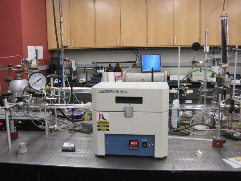
9 CVD System for Graphene Growth

10 Graphene from Solid Carbon Source Nature 468, 549 (2010)


11 Graphene from Girl Scout Cookies

12 SEM Images SEM of the Cu foil after growth of graphene from a Girl Scout cookie. (A) The original frontside of the Cu; (B) (B) The backside of the Cu foil

13 Graphene Derived from Cookies The online price for a 2 inch by 2 inch CVD graphene is 250 dollars. One box of girl scouts cookies weighs 255 g and can be made into 157,800 m 2 graphene, which can cover 29.5 American football fields. The price for that large of graphene will worth 15,290,697,674 dollars. Commercial source of graphene
14
")
15 Graphene Derived from a Different Carbon Source Ar: 500 cm 3 STP min -1 H 2 : 100 cm 3 STP min -1 (Cockroach leg) (Graphene)

16 Graphene on Different Substrates Graphene Glass Graphene Polymer
 SAED pattern, (B) suspended graphene film on a 1 µm diameter hole and (C) the edge of monolayer")
17 TEM Images Figure. Diffraction pattern and TEM images of the cookiederived graphene. (A) SAED pattern, (B) suspended graphene film on a 1 µm diameter hole and (C) the edge of monolayer graphene. Done by Sun, Z
18 XPS of Graphene
19 UV-Vis of Graphene
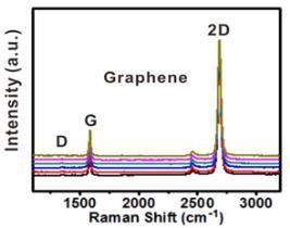
20 Raman Spectra of Graphene 2D 2D 2D D G D G D G 2D 2D 2D D G D G D G
21 Thickness Control The 2D peak, ~2700 cm -1 dominates the monolayer graphene The G peak ~1600 cm -1 dominates multi-layer graphene The D peak ~1350 cm -1 indicates defects and functionalization With Sun

22 1.2 N-Doped Graphene Made from Solid Carbon Sources a c Pristine melamine b pristine graphene d N-doped N-doped graphene With Sun


23 C diffused through nickel form graphene on SiO 2 Graphene grows under the nickel layer Z. Peng*, Z. Yan* et al. ACS Nano 5, 8241 (2011)

24 Growth Mechanism The carbon is expelled as solubility decreases upon cooling
25 Polycrystalline CVD graphene 500 nm 500 nm 0.5 nm Nature 469, 389 (2011)

26 CVD graphene is polycrystalline Synthesis of Wafer-Scale Single-Crystal Graphene Two main methods to reduce graphene seed density: Cu surface pretreatments Electrochemical polishing High-pressure annealing ACS Nano 6, 9110 (2012)

27 Electrochemical Polishing removes surface impurities

28 High-Pressure Annealing flattens the surface Annealing typically in 2 atm absolute pressure of hydrogen for several hours


29 Millimeter-Sized Monolayer Graphene domains grown on Pretreated Cu a b c d Electron diffraction pattern the same for several sites

30 Graphene Domains Transferred on SiO 2 /Si Wafers a b c d

31 Synthesis of Wafer-Scale Single-Crystal Graphene The carrier mobility is as high as cm 2 / V s on SiO 2 /Si substrates at room temperature, comparable to that of exfoliated graphene. a b

32 Graphene Domains across Grain Boundaries of Cu Grain boundaries in the copper do not interfere with growth of the single domain
 30 μm 30 μm 30 μm 30 μm 30 μm 30 μm Z. Yan, Y.")
33 3.2 Bi- and Tri-layer Graphene Single Crystals (graphene pyramids) 30 μm 30 μm 30 μm 30 μm 30 μm 30 μm Z. Yan, Y. Liu et al

34 0-0 Bilayer graphene domains are Bernal-stacked

35 Hexagonal Onion-Ring-like Graphene Domains 100 nm Z. Yan, Y. Liu et al. J. Am. Chem. Soc.135, (2013)
36 Electronic Characterizations 20 μm With Javen

37 Growth Mechanism


38 Growth of Bi, Tri, and Tetralayer Graphene Pristine Cu foil Annealed Cu foil Graphene on Cu foil H 2 H 2, CH C 1000 C Removed some impurities on Cu surface
39 Bernal Graphene 2D Band Fitted with Lorentzians Bilayer graphene fits 4 Lorentzians Trilayer graphene fits 6 Lorentzians Tetralayer graphene fits 3 Lorentzians

40 Visible Spectra of Bi, Tri, and Tetralayer Graphene 2 L 3 L 4 L


41 Electron Diffraction and TEM Images of Bi, Tri, and Tetralayer Graphene Bi: I /I is ~ 3.5 Tri: I /I is ~ 4.5 Tetra: I /I is ~ 6.3
42 Graphene-Dominated Electronic Properties 20 μm With Javen

43 Rebar Graphene-Based Flexible Transparent Electrodes
44 4.2 Metal-Graphene-Carbon Nanotube Multifunctional Hybrids Z. Yan*, L. Ma* et al. ACS Nano 7, 58 (2013)

45 TEM, Raman Characterizations and Length Control Growth on porous nickel foam

46 Field Emission Emitters Turn-on field is around 0.27 V/µm, one of the smallest value ever reported. With Indranil
47 Fuctionalization of Graphene Non-covalent functionalization: π-π interaction, polymer coating Covalent functionalization: Hydrogenation, fluorination, intercalation, oxidation, diazonium chemistry, etc.
48 XPS of F-Graphene C% F% C : F 25 C, 15min :1 50 C, 15min :1 100 C, 15min :1 150 C, 15min :1 200 C, 15min :1 The C : F ratio can be tuned by changing the temperature of fluorination.
49 Raman Spectra of F-Graphene
50 Modulation of Graphene Electronic Properties


 Nat.")
")

 Nano.")
51 Graphene Supperlattice Additional Work Graphene-CNT Bonds Transparent Memory Nat. Commun. 2, 559 (2011) Nat. Commun. 3, 1225 (2012) Nat. Commun. 3, 1101 (2012) Microsupercapcitor Terahertz Spectroscopy Graphene Fibers Nano. Lett. 13, 72 (2013) Nano. Lett. 12, 3711 (2012) Adv. Mater. 25, 4592 (2013)


52 Graphene/Metal Grids for Transparent Electrodes Graphene nanoribbon/sno 2 for Lithium Batteries Graphene nanoribbon for Gas Barriers Thermal Conduction of h-bn Graphene Functionalization Graphene/Metal Grids for Solar Cells CVD Graphene Thickness Control Coal-Derived Graphene Quantum Dots
53 V. Conclusion Both pristine and N-doped graphene could be made from solid carbon sources; Bilayer graphene could be directly grown on insulating substrates; Millimeter-sized monolayer graphene single crystals could be grown on polycrystalline Cu; Graphene domains with special spatial structures, such as hexagonal graphene onions and graphene pyramids, could be synthesized by CVD method on Cu; Planar and vertical graphene/cnts hybrid materials can be fabricated for multifunctional applications; Electronic properties of graphene could be modulated by chemical methods and atom substitution. Review article: Yu Zhu, Dustin K. James, and James M. Tour, New Routes to Graphene, Graphene Oxide and Their Related Applications Adv. Mater. 2012, DOI: /adma

54 Collaborators: Dr. Paul Engel Dr. Pulickel Ajayan Dr. Angel Marti Dr. Zhengzong Sun James M. Tour Research Group Support Sandia National Laboratory Air Force Office of Scientific Research ONR MURI program Dr. Zheng Yan developed the large area single domain graphene and Bernal stacking, and is now at U. Illinois


55
SUPPLEMENTARY INFORMATION. Observation of tunable electrical bandgap in large-area twisted bilayer graphene synthesized by chemical vapor deposition
 SUPPLEMENTARY INFORMATION Observation of tunable electrical bandgap in large-area twisted bilayer graphene synthesized by chemical vapor deposition Jing-Bo Liu 1 *, Ping-Jian Li 1 *, Yuan-Fu Chen 1, Ze-Gao
Session V: Graphene. Matteo Bruna CAMBRIDGE UNIVERSITY DEPARTMENT OF ENGINEERING
 Session V: Graphene Matteo Bruna Graphene: Material in the Flatland Graphite Graphene Properties: Thinnest imaginable material Good(and tunable) electrical conductor Strongest ever measured Stiffest known
Graphene. Tianyu Ye November 30th, 2011
 Graphene Tianyu Ye November 30th, 2011 Outline What is graphene? How to make graphene? (Exfoliation, Epitaxial, CVD) Is it graphene? (Identification methods) Transport properties; Other properties; Applications;
Nanostrukturphysik Übung 2 (Class 3&4)
") Nanostrukturphysik Übung 2 (Class 3&4) Prof. Yong Lei & Dr. Yang Xu 2017.05.03 Fachgebiet 3D-Nanostrukturierung, Institut für Physik Contact: yong.lei@tu-ilmenau.de (3748), yang.xu@tuilmenau.de (4902)
Nanostrukturphysik Übung 2 (Class 3&4) Prof. Yong Lei & Dr. Yang Xu 2017.05.03 Fachgebiet 3D-Nanostrukturierung, Institut für Physik Contact: yong.lei@tu-ilmenau.de (3748), yang.xu@tuilmenau.de (4902)
Wafer-scale fabrication of graphene
 Wafer-scale fabrication of graphene Sten Vollebregt, MSc Delft University of Technology, Delft Institute of Mircosystems and Nanotechnology Delft University of Technology Challenge the future Delft University
Supplementary Figures Supplementary Figure 1
 Supplementary Figures Supplementary Figure 1 Optical images of graphene grains on Cu after Cu oxidation treatment at 200 for 1m 30s. Each sample was synthesized with different H 2 annealing time for (a)
SUPPLEMENTARY INFORMATION
 SUPPLEMENTARY INFORMATION Facile Synthesis of High Quality Graphene Nanoribbons Liying Jiao, Xinran Wang, Georgi Diankov, Hailiang Wang & Hongjie Dai* Supplementary Information 1. Photograph of graphene
Transparent Electrode Applications
 Transparent Electrode Applications LCD Solar Cells Touch Screen Indium Tin Oxide (ITO) Zinc Oxide (ZnO) - High conductivity - High transparency - Resistant to environmental effects - Rare material (Indium)
Graphene films on silicon carbide (SiC) wafers supplied by Nitride Crystals, Inc.
 wafers supplied by Nitride Crystals, Inc.") 9702 Gayton Road, Suite 320, Richmond, VA 23238, USA Phone: +1 (804) 709-6696 info@nitride-crystals.com www.nitride-crystals.com Graphene films on silicon carbide (SiC) wafers supplied by Nitride Crystals,
9702 Gayton Road, Suite 320, Richmond, VA 23238, USA Phone: +1 (804) 709-6696 info@nitride-crystals.com www.nitride-crystals.com Graphene films on silicon carbide (SiC) wafers supplied by Nitride Crystals,
Supporting Information
 Supporting Information Repeated Growth Etching Regrowth for Large-Area Defect-Free Single-Crystal Graphene by Chemical Vapor Deposition Teng Ma, 1 Wencai Ren, 1 * Zhibo Liu, 1 Le Huang, 2 Lai-Peng Ma,
Supplementary Figure S1. AFM images of GraNRs grown with standard growth process. Each of these pictures show GraNRs prepared independently,
 Supplementary Figure S1. AFM images of GraNRs grown with standard growth process. Each of these pictures show GraNRs prepared independently, suggesting that the results is reproducible. Supplementary Figure
Supplementary Figure S1. AFM characterizations and topographical defects of h- BN films on silica substrates. (a) (c) show the AFM height
 (c) show the AFM height") Supplementary Figure S1. AFM characterizations and topographical defects of h- BN films on silica substrates. (a) (c) show the AFM height topographies of h-bn film in a size of ~1.5µm 1.5µm, 30µm 30µm
Supplementary Figure S1. AFM characterizations and topographical defects of h- BN films on silica substrates. (a) (c) show the AFM height topographies of h-bn film in a size of ~1.5µm 1.5µm, 30µm 30µm
Low Voltage Field Emission SEM (LV FE-SEM): A Promising Imaging Approach for Graphene Samples
: A Promising Imaging Approach for Graphene Samples") Low Voltage Field Emission SEM (LV FE-SEM): A Promising Imaging Approach for Graphene Samples Jining Xie Agilent Technologies May 23 rd, 2012 www.agilent.com/find/nano Outline 1. Introduction 2. Agilent
Low Voltage Field Emission SEM (LV FE-SEM): A Promising Imaging Approach for Graphene Samples Jining Xie Agilent Technologies May 23 rd, 2012 www.agilent.com/find/nano Outline 1. Introduction 2. Agilent
Supplementary Information
 Supplementary Information Supplementary Figure 1. fabrication. A schematic of the experimental setup used for graphene Supplementary Figure 2. Emission spectrum of the plasma: Negative peaks indicate an
Grpahene Synthesis by CVD. QingkaiYu Ingram School of Engineering Texas State University at San Marcos
 Grpahene Synthesis by CVD QingkaiYu Ingram School of Engineering Texas State University at San Marcos @ Applied Nanotech Inc, July 25 th, 2011 Acknowledgement Texas State University Dr. Zhihong Liu Austin
A new method of growing graphene on Cu by hydrogen etching
 A new method of growing graphene on Cu by hydrogen etching Linjie zhan version 6, 2015.05.12--2015.05.24 CVD graphene Hydrogen etching Anisotropic Copper-catalyzed Highly anisotropic hydrogen etching method
Supplementary Figure 1. Electron micrographs of graphene and converted h-bn. (a) Low magnification STEM-ADF images of the graphene sample before
 Low magnification STEM-ADF images of the graphene sample before") Supplementary Figure 1. Electron micrographs of graphene and converted h-bn. (a) Low magnification STEM-ADF images of the graphene sample before conversion. Most of the graphene sample was folded after
Supplementary Figure 1. Electron micrographs of graphene and converted h-bn. (a) Low magnification STEM-ADF images of the graphene sample before conversion. Most of the graphene sample was folded after
STM and graphene. W. W. Larry Pai ( 白偉武 ) Center for condensed matter sciences, National Taiwan University NTHU, 2013/05/23
 Center for condensed matter sciences, National Taiwan University NTHU, 2013/05/23") STM and graphene W. W. Larry Pai ( 白偉武 ) Center for condensed matter sciences, National Taiwan University NTHU, 2013/05/23 Why graphene is important: It is a new form of material (two dimensional, single
STM and graphene W. W. Larry Pai ( 白偉武 ) Center for condensed matter sciences, National Taiwan University NTHU, 2013/05/23 Why graphene is important: It is a new form of material (two dimensional, single
Initial Stages of Growth of Organic Semiconductors on Graphene
 Initial Stages of Growth of Organic Semiconductors on Graphene Presented by: Manisha Chhikara Supervisor: Prof. Dr. Gvido Bratina University of Nova Gorica Outline Introduction to Graphene Fabrication
Supplementary Information
 Supplementary Information Chemical and Bandgap Engineering in Monolayer Hexagonal Boron Nitride Kun Ba 1,, Wei Jiang 1,,Jingxin Cheng 2, Jingxian Bao 1, Ningning Xuan 1,Yangye Sun 1, Bing Liu 1, Aozhen
Graphene Fundamentals and Emergent Applications
 Graphene Fundamentals and Emergent Applications Jamie H. Warner Department of Materials University of Oxford Oxford, UK Franziska Schaffel Department of Materials University of Oxford Oxford, UK Alicja
SUPPLEMENTARY INFORMATION
 Direct Visualization of Large-Area Graphene Domains and Boundaries by Optical Birefringency Dae Woo Kim 1,*, Yun Ho Kim 1,2,*, Hyeon Su Jeong 1, Hee-Tae Jung 1 * These authors contributed equally to this
Layer-modulated synthesis of uniform tungsten disulfide nanosheet using gas-phase precursors.
 Layer-modulated synthesis of uniform tungsten disulfide nanosheet using gas-phase precursors. Jusang Park * Hyungjun Kim School of Electrical and Electronics Engineering, Yonsei University, 262 Seongsanno,
Supplementary Figure 1 Experimental setup for crystal growth. Schematic drawing of the experimental setup for C 8 -BTBT crystal growth.
 Supplementary Figure 1 Experimental setup for crystal growth. Schematic drawing of the experimental setup for C 8 -BTBT crystal growth. Supplementary Figure 2 AFM study of the C 8 -BTBT crystal growth
Part II. Introduction of Graphene
 Part II. Introduction of Graphene 1 Graphene (Mother of all graphitic form) 2D honeycomb lattice Graphene 0D 1D 3D bulky bll ball Nanotube Graphite Geims et al, Nature Materials,Vol.6 183, 2007 2 History
Graphene Chemical Vapor Deposition (CVD) Growth
 Growth") ECE440 Nanoelectronics Graphene Chemical Vapor Deposition (CVD) Growth Zheng Yang Timeline of graphene CVD growth Exfoliation
ECE440 Nanoelectronics Graphene Chemical Vapor Deposition (CVD) Growth Zheng Yang Timeline of graphene CVD growth Exfoliation
Halbleiter Prof. Yong Lei Prof. Thomas Hannappel
 Halbleiter Prof. Yong Lei Prof. Thomas Hannappel yong.lei@tu-ilmenau.de thomas.hannappel@tu-ilmenau.de http:///nanostruk/ Organic semiconductors Small-molecular materials Rubrene Pentacene Polymers PEDOT:PSS
Carbon Nanomaterials: Nanotubes and Nanobuds and Graphene towards new products 2030
 Carbon Nanomaterials: Nanotubes and Nanobuds and Graphene towards new products 2030 Prof. Dr. Esko I. Kauppinen Helsinki University of Technology (TKK) Espoo, Finland Forecast Seminar February 13, 2009
Nanostrukturphysik (Nanostructure Physics)
") Nanostrukturphysik (Nanostructure Physics) Prof. Yong Lei & Dr. Yang Xu Fachgebiet 3D-Nanostrukturierung, Institut für Physik Contact: yong.lei@tu-ilmenau.de; yang.xu@tu-ilmenau.de Office: Unterpoerlitzer
Nanostrukturphysik (Nanostructure Physics) Prof. Yong Lei & Dr. Yang Xu Fachgebiet 3D-Nanostrukturierung, Institut für Physik Contact: yong.lei@tu-ilmenau.de; yang.xu@tu-ilmenau.de Office: Unterpoerlitzer
Supplementary Figures
 Supplementary Figures 1500 Heating Annealing Growing Cooling 20 Temperature ( o C) 1000 500 Ar:H 2 = 5:1 Ar:H 2 = 5:1 15 10 5 Pressure(Pa) 0 Ar(SiH 4 (5%)):C 2 H 2 = 1:2 120 mins 5 mins 5 40 mins ~120
Evolution of graphene growth on Cu and Ni studied by carbon isotope
 Evolution of graphene growth on Cu and Ni studied by carbon isotope labeling Xuesong Li a, Weiwei Cai a, Luigi Colombo b*, and Rodney S. Ruoff a* Large-area graphene is a new material with properties that
Nanostrukturphysik (Nanostructure Physics)
") Nanostrukturphysik (Nanostructure Physics) Prof. Yong Lei & Dr. Yang Xu Fachgebiet 3D-Nanostrukturierung, Institut für Physik Contact: yong.lei@tu-ilmenau.de; yang.xu@tu-ilmenau.de Office: Unterpoerlitzer
Nanostrukturphysik (Nanostructure Physics) Prof. Yong Lei & Dr. Yang Xu Fachgebiet 3D-Nanostrukturierung, Institut für Physik Contact: yong.lei@tu-ilmenau.de; yang.xu@tu-ilmenau.de Office: Unterpoerlitzer
Supporting Information. Fast Synthesis of High-Performance Graphene by Rapid Thermal Chemical Vapor Deposition
 1 Supporting Information Fast Synthesis of High-Performance Graphene by Rapid Thermal Chemical Vapor Deposition Jaechul Ryu, 1,2, Youngsoo Kim, 4, Dongkwan Won, 1 Nayoung Kim, 1 Jin Sung Park, 1 Eun-Kyu
Graphene Novel Material for Nanoelectronics
 Graphene Novel Material for Nanoelectronics Shintaro Sato Naoki Harada Daiyu Kondo Mari Ohfuchi (Manuscript received May 12, 2009) Graphene is a flat monolayer of carbon atoms with a two-dimensional honeycomb
Supplementary Information for
 Supplementary Information for Highly Stable, Dual-Gated MoS 2 Transistors Encapsulated by Hexagonal Boron Nitride with Gate-Controllable Contact Resistance and Threshold Voltage Gwan-Hyoung Lee, Xu Cui,
Supporting Information for
 Supporting Information for Multilayer CuO@NiO Hollow Spheres: Microwave-Assisted Metal-Organic-Framework Derivation and Highly Reversible Structure-Matched Stepwise Lithium Storage Wenxiang Guo, Weiwei
The goal of this project is to enhance the power density and lowtemperature efficiency of solid oxide fuel cells (SOFC) manufactured by atomic layer
 manufactured by atomic layer") Stanford University Michael Shandalov1, Shriram Ramanathan2, Changhyun Ko2 and Paul McIntyre1 1Department of Materials Science and Engineering, Stanford University 2Division of Engineering and Applied
Stanford University Michael Shandalov1, Shriram Ramanathan2, Changhyun Ko2 and Paul McIntyre1 1Department of Materials Science and Engineering, Stanford University 2Division of Engineering and Applied
Supplementary Figure 1 Magneto-transmission spectra of graphene/h-bn sample 2 and Landau level transition energies of three other samples.
 Supplementary Figure 1 Magneto-transmission spectra of graphene/h-bn sample 2 and Landau level transition energies of three other samples. (a,b) Magneto-transmission ratio spectra T(B)/T(B 0 ) of graphene/h-bn
Supplementary Information for. Origin of New Broad Raman D and G Peaks in Annealed Graphene
 Supplementary Information for Origin of New Broad Raman D and G Peaks in Annealed Graphene Jinpyo Hong, Min Kyu Park, Eun Jung Lee, DaeEung Lee, Dong Seok Hwang and Sunmin Ryu* Department of Applied Chemistry,
performance electrocatalytic or electrochemical devices. Nanocrystals grown on graphene could have
 Nanocrystal Growth on Graphene with Various Degrees of Oxidation Hailiang Wang, Joshua Tucker Robinson, Georgi Diankov, and Hongjie Dai * Department of Chemistry and Laboratory for Advanced Materials,
Engineered Flexible Conductive Barrier Films for Advanced Energy Devices
 The 13 th Korea-U.S. Forum on Nanotechnology Engineered Flexible Conductive Barrier Films for Advanced Energy Devices Jinsung Kwak 1, Yongsu Jo 1, Soon-Dong Park 2, Na Yeon Kim 1, Se-Yang Kim 1, Zonghoon
Transient Photocurrent Measurements of Graphene Related Materials
 Transient Photocurrent Measurements of Graphene Related Materials P. Srinivasa Rao Mentor: Prof. dr. Gvido Bratina Laboratory of Organic Matter Physics University of Nova Gorica 1 Contents: 1. Electrical
A. Optimizing the growth conditions of large-scale graphene films
 1 A. Optimizing the growth conditions of large-scale graphene films Figure S1. Optical microscope images of graphene films transferred on 300 nm SiO 2 /Si substrates. a, Images of the graphene films grown
2D Materials for Gas Sensing
 2D Materials for Gas Sensing S. Guo, A. Rani, and M.E. Zaghloul Department of Electrical and Computer Engineering The George Washington University, Washington DC 20052 Outline Background Structures of
Novel Tooling for Scaling of High Quality CVD Graphene Production. Karlheinz Strobl, Mathieu Monville, Riju Singhal and Samuel Wright
 Novel Tooling for Scaling of High Quality CVD Graphene Production Karlheinz Strobl, Mathieu Monville, Riju Singhal and Samuel Wright 1 Commercialization of Nano Materials Commercialization Volume production
Optical Science of Nano-graphene (graphene oxide and graphene quantum dot) Introduction of optical properties of nano-carbon materials
 Introduction of optical properties of nano-carbon materials") Optical Science of Nano-graphene (graphene oxide and graphene quantum dot) J Kazunari Matsuda Institute of Advanced Energy, Kyoto University Introduction of optical properties of nano-carbon materials
Optical Science of Nano-graphene (graphene oxide and graphene quantum dot) J Kazunari Matsuda Institute of Advanced Energy, Kyoto University Introduction of optical properties of nano-carbon materials
Title of file for HTML: Supplementary Information Description: Supplementary Figures and Supplementary References
 Title of file for HTML: Supplementary Information Description: Supplementary Figures and Supplementary References Supplementary Figure 1. SEM images of perovskite single-crystal patterned thin film with
Wafer Scale Homogeneous Bilayer Graphene Films by. Chemical Vapor Deposition
 Supporting Information for Wafer Scale Homogeneous Bilayer Graphene Films by Chemical Vapor Deposition Seunghyun Lee, Kyunghoon Lee, Zhaohui Zhong Department of Electrical Engineering and Computer Science,
Chapter 2 Synthesis, Structure, and Properties of Graphene and Graphene Oxide
 Chapter 2 Synthesis, Structure, and Properties of Graphene and Graphene Oxide 2.1 Introduction To develop large-area graphene-based TCFs, one of the foremost challenges is to produce sufficient amounts
Supporting Information
 Copyright WILEY-VCH Verlag GmbH & Co. KGaA, 69469 Weinheim, Germany, 2015. Supporting Information for Adv. Mater., DOI: 10.1002/adma.201502134 Stable Metallic 1T-WS 2 Nanoribbons Intercalated with Ammonia
Introduction to Nanotechnology Chapter 5 Carbon Nanostructures Lecture 1
 Introduction to Nanotechnology Chapter 5 Carbon Nanostructures Lecture 1 ChiiDong Chen Institute of Physics, Academia Sinica chiidong@phys.sinica.edu.tw 02 27896766 Section 5.2.1 Nature of the Carbon Bond
Supplementary Figure 1 Dark-field optical images of as prepared PMMA-assisted transferred CVD graphene films on silicon substrates (a) and the one
 and the one") Supplementary Figure 1 Dark-field optical images of as prepared PMMA-assisted transferred CVD graphene films on silicon substrates (a) and the one after PBASE monolayer growth (b). 1 Supplementary Figure
Supplementary Figure 1 Dark-field optical images of as prepared PMMA-assisted transferred CVD graphene films on silicon substrates (a) and the one after PBASE monolayer growth (b). 1 Supplementary Figure
Supplementary Information
 Supplementary Information Plasma-assisted reduction of graphene oxide at low temperature and atmospheric pressure for flexible conductor applications Seung Whan Lee 1, Cecilia Mattevi 2, Manish Chhowalla
Supporting Information
 Electronic Supplementary Material (ESI) for Journal of Materials Chemistry A. This journal is The Royal Society of Chemistry 2017 Supporting Information NiSe 2 Pyramids Deposited on N-doped Graphene Encapsulated
Supporting Information Available:
 Supporting Information Available: Photoresponsive and Gas Sensing Field-Effect Transistors based on Multilayer WS 2 Nanoflakes Nengjie Huo 1, Shengxue Yang 1, Zhongming Wei 2, Shu-Shen Li 1, Jian-Bai Xia
Controllable Growth of the Graphene from Millimeter-Sized Monolayer to Multilayer on Cu by Chemical Vapor Deposition
 Liu et al. Nanoscale Research Letters (2015) 10:455 DOI 10.1186/s11671-015-1164-0 NANO EXPRESS Controllable Growth of the Graphene from Millimeter-Sized Monolayer to Multilayer on Cu by Chemical Vapor
Three-dimensional flexible and conductive interconnected graphene networks grown by chemical vapour deposition
 SUPPLEMENTARY INFORMATION Three-dimensional flexible and conductive interconnected graphene networks grown by chemical vapour deposition S1. Characterization of the graphene foam (GF) and GF/PDMS composites
Nanotechnology in Consumer Products
 Nanotechnology in Consumer Products June 17, 2015 October 31, 2014 The webinar will begin at 1pm Eastern Time Perform an audio check by going to Tools > Audio > Audio Setup Wizard Chat Box Chat Box Send
III-V nanostructured materials synthesized by MBE droplet epitaxy
 III-V nanostructured materials synthesized by MBE droplet epitaxy E.A. Anyebe 1, C. C. Yu 1, Q. Zhuang 1,*, B. Robinson 1, O Kolosov 1, V. Fal ko 1, R. Young 1, M Hayne 1, A. Sanchez 2, D. Hynes 2, and
Supplementary Figure 1 A schematic representation of the different reaction mechanisms
 Supplementary Figure 1 A schematic representation of the different reaction mechanisms observed in electrode materials for lithium batteries. Black circles: voids in the crystal structure, blue circles:
Low Temperature Plasma CVD Grown Graphene by Microwave Surface-Wave Plasma CVD Using Camphor Precursor
 Journal of Physical Science and Application 6 (2) (2016) 34-38 doi: 10.17265/2159-5348/2016.02.005 D DAVID PUBLISHING Low Temperature Plasma CVD Grown Graphene by Microwave Surface-Wave Plasma CVD Using
Supplementary Figures
 Supplementary Figures Supplementary Figure 1: Microstructure, morphology and chemical composition of the carbon microspheres: (a) A SEM image of the CM-NFs; and EDS spectra of CM-NFs (b), CM-Ns (d) and
SUPPLEMENTARY INFORMATION
 Lateral heterojunctions within monolayer MoSe 2 -WSe 2 semiconductors Chunming Huang 1,#,*, Sanfeng Wu 1,#,*, Ana M. Sanchez 2,#,*, Jonathan J. P. Peters 2, Richard Beanland 2, Jason S. Ross 3, Pasqual
Chemical Vapor Deposition Graphene Grown on Peeled- Off Epitaxial Cu(111) Foil: A Simple Approach to Improved Properties
 Foil: A Simple Approach to Improved Properties") Supplementary information Chemical Vapor Deposition Graphene Grown on Peeled- Off Epitaxial Cu(111) Foil: A Simple Approach to Improved Properties Hak Ki Yu 1,2, Kannan Balasubramanian 3, Kisoo Kim 4,
Supplementary information Chemical Vapor Deposition Graphene Grown on Peeled- Off Epitaxial Cu(111) Foil: A Simple Approach to Improved Properties Hak Ki Yu 1,2, Kannan Balasubramanian 3, Kisoo Kim 4,
Multicolor Graphene Nanoribbon/Semiconductor Nanowire. Heterojunction Light-Emitting Diodes
 Multicolor Graphene Nanoribbon/Semiconductor Nanowire Heterojunction Light-Emitting Diodes Yu Ye, a Lin Gan, b Lun Dai, *a Hu Meng, a Feng Wei, a Yu Dai, a Zujin Shi, b Bin Yu, a Xuefeng Guo, b and Guogang
Carbon Nanotubes: Development of Nanomaterials for Hydrogen Storage
 Carbon Nanotubes: Development of Nanomaterials for Hydrogen Storage Hongjie Dai Department of Chemistry & Laboratory for Advanced Materials Stanford University GCEP, September 19, 2006 Outline Can carbon
Overview. Carbon in all its forms. Background & Discovery Fabrication. Important properties. Summary & References. Overview of current research
 Graphene Prepared for Solid State Physics II Pr Dagotto Spring 2009 Laurene Tetard 03/23/09 Overview Carbon in all its forms Background & Discovery Fabrication Important properties Overview of current
Supplemental Information. Crumpled Graphene Balls Stabilized. Dendrite-free Lithium Metal Anodes
 JOUL, Volume 2 Supplemental Information Crumpled Graphene Balls Stabilized Dendrite-free Lithium Metal Anodes Shan Liu, Aoxuan Wang, Qianqian Li, Jinsong Wu, Kevin Chiou, Jiaxing Huang, and Jiayan Luo
ConceptGraphene. Small or medium-scale focused research project. WP1 Fabrication
 ConceptGraphene New Electronics Concept: Wafer-Scale Epitaxial Graphene Small or medium-scale focused research project WP1 Fabrication Deliverable 1.2 Quality comparison: epitaxial graphene vs graphene
Conference Return Seminar- NANO2014,Moscow State University,Moscow,Russia Date: th July 2014
 Conference Return Seminar- NANO2014,Moscow State University,Moscow,Russia Date:13-1818 th July 2014 An electrochemical method for the synthesis of single and few layers graphene sheets for high temperature
Supporting Information
 Supporting Information Direct Chemical Vapor Deposition-Derived Graphene Glasses Targeting Wide Ranged Applications Jingyu Sun, Yubin Chen, Manish Kr. Priydarshi, Zhang Chen, Alicja Bachmatiuk,, Zhiyu
Elastic properties of graphene
 Elastic properties of graphene M. I. Katsnelson P. Le Doussal B. Horowitz K. Wiese J. Gonzalez P. San-Jose V. Parente B. Amorim R. Roldan C. Gomez-Navarro J. Gomez G. Lopez-Polin F. Perez-Murano A. Morpurgo
Chapter 1 Introduction
 Chapter 1 Introduction In our planet carbon forms the basis of all organic molecules which makes it the most important element of life. It is present in over 95% of the known chemical compounds overall
SUPPLEMENTARY INFORMATION
 DOI: 10.1038/NCHEM.1421 Understanding and Controlling the Substrate Effect on Graphene Electron-Transfer Chemistry via Reactivity Imprint Lithography Qing Hua Wang, Zhong Jin, Ki Kang Kim, Andrew J. Hilmer,
Large Scale Direct Synthesis of Graphene on Sapphire and Transfer-free Device Fabrication
 Supplementary Information Large Scale Direct Synthesis of Graphene on Sapphire and Transfer-free Device Fabrication Hyun Jae Song a, Minhyeok Son a, Chibeom Park a, Hyunseob Lim a, Mark P. Levendorf b,
Lectures Graphene and
 Lectures 15-16 Graphene and carbon nanotubes Graphene is atomically thin crystal of carbon which is stronger than steel but flexible, is transparent for light, and conducts electricity (gapless semiconductor).
Carbon based Nanoscale Electronics
 Carbon based Nanoscale Electronics 09 02 200802 2008 ME class Outline driving force for the carbon nanomaterial electronic properties of fullerene exploration of electronic carbon nanotube gold rush of
Supplementary Figure 1. (a-b) EDX of Mo 2 and Mo 2
 EDX of Mo 2 and Mo 2") Supplementary Figure 1. (a-b) EDX of Mo 2 C@NPC/NPRGO and Mo 2 C@NPC. Supplementary Figure 2. (a) SEM image of PMo 12 2-PPy, (b) TEM, (c) HRTEM, (d) STEM image and EDX elemental mapping of C, N, P, and
Supplementary Figure 1. (a-b) EDX of Mo 2 C@NPC/NPRGO and Mo 2 C@NPC. Supplementary Figure 2. (a) SEM image of PMo 12 2-PPy, (b) TEM, (c) HRTEM, (d) STEM image and EDX elemental mapping of C, N, P, and
Understanding Irreducible and Reducible Oxides as Catalysts for Carbon Nanotubes and Graphene Formation
 Wright State University CORE Scholar Special Session 5: Carbon and Oxide Based Nanostructured Materials (2011) Special Session 5 6-2011 Understanding Irreducible and Reducible Oxides as Catalysts for Carbon
Direct Measurement of Adhesion Energy of Monolayer Graphene As-Grown. on Copper and Its Application to Renewable Transfer Process
 SUPPORTING INFORMATION Direct Measurement of Adhesion Energy of Monolayer Graphene As-Grown on Copper and Its Application to Renewable Transfer Process Taeshik Yoon 1, Woo Cheol Shin 2, Taek Yong Kim 2,
30-Inch Roll-Based Production of High-Quality Graphene Films for Flexible Transparent Electrodes
 30-Inch Roll-Based Production of High-Quality Graphene Films for Flexible Transparent Electrodes Sukang Bae, 1* Hyeong Keun Kim, 3* Xianfang Xu, 5 Jayakumar Balakrishnan, 5 Tian Lei, 1 Young Il Song, 6
A Novel Approach to the Layer Number-Controlled and Grain Size- Controlled Growth of High Quality Graphene for Nanoelectronics
 Supporting Information A Novel Approach to the Layer Number-Controlled and Grain Size- Controlled Growth of High Quality Graphene for Nanoelectronics Tej B. Limbu 1,2, Jean C. Hernández 3, Frank Mendoza
Supporting Information
 Copyright WILEY-VCH Verlag GmbH & Co. KGaA, 69469 Weinheim, Germany, 2017. Supporting Information for Adv. Energy Mater., DOI: 10.1002/aenm.201701456 Selective Etching of Nitrogen-Doped Carbon by Steam
Optimizing Graphene Morphology on SiC(0001)
") Optimizing Graphene Morphology on SiC(0001) James B. Hannon Rudolf M. Tromp Graphene sheets Graphene sheets can be formed into 0D,1D, 2D, and 3D structures Chemically inert Intrinsically high carrier mobility
Optimizing Graphene Morphology on SiC(0001) James B. Hannon Rudolf M. Tromp Graphene sheets Graphene sheets can be formed into 0D,1D, 2D, and 3D structures Chemically inert Intrinsically high carrier mobility
Solutions for Assignment-8
 Solutions for Assignment-8 Q1. The process of adding impurities to a pure semiconductor is called: [1] (a) Mixing (b) Doping (c) Diffusing (d) None of the above In semiconductor production, doping intentionally
SUPPLEMENTARY INFORMATION
 Topological insulator nanostructures for near-infrared transparent flexible electrodes Hailin Peng 1*, Wenhui Dang 1, Jie Cao 1, Yulin Chen 2,3, Di Wu 1, Wenshan Zheng 1, Hui Li 1, Zhi-Xun Shen 3,4, Zhongfan
Graphene: the Route from Touch Screens to Digital Nanoelectronics
 Graphene: the Route from Touch Screens to Digital Nanoelectronics László Péter Biró Research Institute for Technical Physics & Materials Science, Budapest, Hungary http://www.nanotechnology.hu/ Human History
Enhanced photocurrent of ZnO nanorods array sensitized with graphene. quantum dots
 Electronic Supplementary Material (ESI) for RSC Advances. This journal is The Royal Society of Chemistry 2015 Enhanced photocurrent of ZnO nanorods array sensitized with graphene quantum dots Bingjun Yang,
Supporting Information. 1T-Phase MoS 2 Nanosheets on TiO 2 Nanorod Arrays: 3D Photoanode with Extraordinary Catalytic Performance
 Supporting Information 1T-Phase MoS 2 Nanosheets on Nanorod Arrays: 3D Photoanode with Extraordinary Catalytic Performance Yuxi Pi, Zhen Li, Danyun Xu, Jiapeng Liu, Yang Li, Fengbao Zhang, Guoliang Zhang,
Modulation-Doped Growth of Mosaic Graphene with Single Crystalline. p-n Junctions for Efficient Photocurrent Generation
 Modulation-Doped Growth of Mosaic Graphene with Single Crystalline p-n Junctions for Efficient Photocurrent Generation Kai Yan 1,, Di Wu 1,, Hailin Peng 1, *, Li Jin 2, Qiang Fu 2, Xinhe Bao 2 and Zhongfan
Recap (so far) Low-Dimensional & Boundary Effects
 Low-Dimensional & Boundary Effects") Recap (so far) Ohm s & Fourier s Laws Mobility & Thermal Conductivity Heat Capacity Wiedemann-Franz Relationship Size Effects and Breakdown of Classical Laws 1 Low-Dimensional & Boundary Effects Energy
Recap (so far) Ohm s & Fourier s Laws Mobility & Thermal Conductivity Heat Capacity Wiedemann-Franz Relationship Size Effects and Breakdown of Classical Laws 1 Low-Dimensional & Boundary Effects Energy
Supporting Information. Direct Growth of Graphene Films on 3D Grating. Structural Quartz Substrates for High-performance. Pressure-Sensitive Sensor
 Supporting Information Direct Growth of Graphene Films on 3D Grating Structural Quartz Substrates for High-performance Pressure-Sensitive Sensor Xuefen Song, a,b Tai Sun b Jun Yang, b Leyong Yu, b Dacheng
Supplementary Figure S1. Raman M bands of few-layer graphene. (a) The M band for the pristine bilayer, trilayer and tetralayer graphene.
 The M band for the pristine bilayer, trilayer and tetralayer graphene.") Supplementary Figure S1. Raman M bands of few-layer graphene. (a) The M band for the pristine bilayer, trilayer and tetralayer graphene. (b) The M band for the triazine decorated trilayer graphene. (c)
Supplementary Figure S1. Raman M bands of few-layer graphene. (a) The M band for the pristine bilayer, trilayer and tetralayer graphene. (b) The M band for the triazine decorated trilayer graphene. (c)
Selective Manipulation of Molecules by Electrostatic Force and Detection of Single Molecules in Aqueous Solution
 Supporting Information Selective Manipulation of Molecules by Electrostatic Force and Detection of Single Molecules in Aqueous Solution Zhongbo Yan, Ming Xia, Pei Zhang, and Ya-Hong Xie* Department of
Center for Integrated Nanostructure Physics (CINAP)
") Center for Integrated Nanostructure Physics (CINAP) - Institute for Basic Science (IBS) was launched in 2012 by the Korean government to promote basic science in Korea - Our Center was established in 2012
Center for Integrated Nanostructure Physics (CINAP) - Institute for Basic Science (IBS) was launched in 2012 by the Korean government to promote basic science in Korea - Our Center was established in 2012
2D MBE Activities in Sheffield. I. Farrer, J. Heffernan Electronic and Electrical Engineering The University of Sheffield
 2D MBE Activities in Sheffield I. Farrer, J. Heffernan Electronic and Electrical Engineering The University of Sheffield Outline Motivation Van der Waals crystals The Transition Metal Di-Chalcogenides
Figure 1: Graphene release, transfer and stacking processes. The graphene stacking began with CVD
 Supplementary figure 1 Graphene Growth and Transfer Graphene PMMA FeCl 3 DI water Copper foil CVD growth Back side etch PMMA coating Copper etch in 0.25M FeCl 3 DI water rinse 1 st transfer DI water 1:10
Hydrothermally Activated Graphene Fiber Fabrics for Textile. Electrodes of Supercapacitors
 Supporting Information for Hydrothermally Activated Graphene Fiber Fabrics for Textile Electrodes of Supercapacitors Zheng Li, Tieqi Huang, Weiwei Gao*, Zhen Xu, Dan Chang, Chunxiao Zhang, and Chao Gao*
Omnidirectionally Stretchable and Transparent Graphene Electrodes
 Supporting Information for: Omnidirectionally Stretchable and Transparent Graphene Electrodes Jin Yong Hong,, Wook Kim, Dukhyun Choi, Jing Kong,*, and Ho Seok Park*, School of Chemical Engineering, Sungkyunkwan
Chemical Vapour Deposition of Large-area High-quality Graphene Films for Electronic Applications
 Chemical Vapour Deposition of Large-area High-quality Graphene Films for Electronic Applications Kai WANG A thesis submitted to Imperial College London In fulfilment of the requirements for the degree