Electrical Standards based on quantum effects: Part II. Beat Jeckelmann
|
|
|
- Derek Lambert Long
- 5 years ago
- Views:
Transcription


1 Electrical Standards based on quantum effects: Part II Beat Jeckelmann

2 Part II: The Quantum Hall Effect Overview Classical Hall effect Two-dimensional electron gas Landau levels Measurement technique Accuracy of the quantized Hall resistance Applications in dc and ac electrical metrology 2


3 Discovery of the Quantum Hall Effect K. Von Klitzing discovers the quantum Hall effect in on 5 February 1980 in Grenoble K. v. Klitzing et al, Phys. Rev. Lett., 45, 494 (1980) 3
 4")
4 Classical Hall effect (1879) X X X X BX v X X X X X -e X X X X X F L X X X X X X X X X X Lorentz Force F L q v B Edwin Hall ( ) 4
5 Classical Hall effect (2) V H d F m F e U H n B I e d 3D I n 3D : carrier concentration 2D-system: U H B I ne Hall effect independent of geometrical dimensions! 5
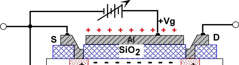
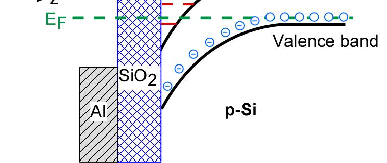
6 Realisation of a 2D electron gas Si MOSFET 6


7 GaAs Heterostructure Layers grown by: Molecular Beam Epitaxy (MBE) or Metal Organic Chemical Beam Epitaxy (MOVCD) 4 mm 7
8 Inversion Layer E E 1 de Broglie wavelength: typically 100 nm (GaAs) E 0 E F Conduction band level spacing at 10 T: Si: 7.9 mev GaAs: 17 mev Graphene: 120 mev z (nm) thermal energy: T = 4 K: kt = 0.36 mev 8
9 Landau levels c cyclotron motion in a strong magnetic field Classical: r c c v r c e B m z Quantum mechanics: Energy values of closed orbits E 1 E0 cn, n 2 0,1, 2, 3... (spin neglected) magnetic length: (8 10 T) r c l 2n 1, l e B 9
10 Landau quantization (2) E Orbital degeneracy N L w 2 2l Number of states in a Landau level State density n B 1 2l 2 eb h Number of flux quanta within the area of the sample B = 0 B z >0 no scattering Filling factor: i n n B s 10
11 Quantum Hall effect? Hall voltage in a 2D-system: U H B I n e s R H B i n B e h, 2 e i i 1, 2, 3... observed when i levels are fully occupied! 11
12 Mobility gap Fermi level mobility gap Disorder and scattering removes orbital degeneracy Localized states do not carry current extended states localized states Plateau forms when E F resides within the localized states B z >0 no scattering B z >0 scattering state density Varenna 2016 / El. Standards II 14
13 QHE in a real device V H I V H + V c 15
14 QHE in a real device (2) E electronic states at Fermi energy E F -L y /2 o +L y /2 No energy gaps for real devices with finite width 16
15 Edge state picture Skipping Orbits source and drain contact are connected by a common edge one-dimensional edge channels carry the current Landauer formalism current = driving force of electronic transport Varenna 2016 / El. Standards II 17
16 Büttiker formalism Current in 1D channels: 5 R 5, T 5 R 6, T 6 6 I h e I R 1 T 1 R 2 T 2 : difference electrochemical potential R 3, T 3 R 4, T 4 R H R i xx 5 3 e 4 3 e i e i e h h 1 2 h i e 0 2 T: transmission R: reflection coefficient T i = 1, R i =0 ; Varenna 2016 / El. Standards II 6 18
17 QHE Model The QHE is a collective phenomenon, it can not be explained by a microscopic model A vanishing longitudinal resistivity indicated the absence of backscattering Under this condition, the QHE is the direct consequence of the transmission of one-dimensional channels. 19


18 QHE in Graphene Graphene: 2D crystal of carbon atoms with charge carriers» massless relativistic particles Geim & Novoselov Nobel Prize in Physics (2010) 20


19 Unconventional quantum Hall effect xy 4 e 2 1 N h 2 Novoselov, et al, Nature 438,

20 E / mev Interest for graphene E required for accuracy of R H at T B / T Potential to develop a quantum Hall resistance standard At T >5 K and B < 5 T Cryogen-free and cheap 22
21 Fine structure constant R K e h 2 0c 2 Test the validity of RK i RH (i) or: additional route to the determination of independent of QED) most accurate value for : measurement of a e + theoretical expansion of a e in a series expansion of (numerical computations: Kinoshita et al.) 23


22 Fine structure constant R K h e 2 0c 2 a e : Anomalous magnetic moment of e µ Mu : Ground state hyperfine splitting G 90 : Gyro-magnetic moment of the proton h/m: Neutron diffraction; cold atoms.. R K : QHE QED theory necessary without QED 24
23 Metrological application Ideal systems: T = 0 K, I = 0 A No dissipation: R xx = 0 R H i h i e 2 R i K R K is a universal quantity Localization theory, Edge state model Real experiment: T > 0.3 K, I = 40 µa Non-ideal samples Dissipation: R xx > 0 R H i, R 0?? xx Is R H (i) a universal quantity? Independent of device material, mobility, carrier density, plateau index, contact properties...? Few quantitative theoretical models available empirical approach, h i e precision measurements 2 25


24 QHE devices for metrology Carrier concentration B i n s e R H i m -2 < n s < m -2 n s > m -2 : 2nd subband fills up Mobility: > 10 T -1 to have clear separation of the LL up to plateau 4 Hall bar defined by photolithography and wet etching techniques Alloyed AuGeNi contacts 26
25 R H (kw QHE in a real device R H h i e 2 i = DEG B z I R xx (kw B (T)
26 Temperature dependence Thermal activation: 1 K T 10 K electrons thermally activated to the nearest extended states xx T 0 xx e kt E F E LL xy T xy (T) ie2 h xy (T) s xx (T) Cage et al. 1984: 1.2 K < T < 4.2 K, 2 GaAs samples, i = < s <
27 Current dependence GaAs T = 0.3 K i = 2 W = 400 µm Breakdown 29
28 Measurement technique To make use of the QHE for metrological applications, a measurement technique, capable of transferring the QHR to room temperature resistance standards must be available. Most accurate resistance bridge technique: Cryogenic Current Comparator (CCC) 30

29 The cryogenic current comparator (CCC): Principles Meissner effect: Harvey 1972 SQUID Harvey 1972 n 1I1 n2i 2 31

30 The CCC bridge: SQUID: N P I P N S I S (1 d) Detector: with d N t N S R L R L R H U m R S I S R P I P R P R S N P 1 N S 1 d 1 1 U m U 32

31 Ratio accuracy: W 1 N(1 w 1 ) W 2 N(1 w 2 ) U SQUID (w 1 w 2 ) Windings in a binary series: 1, 1, 2, 4, 8, 10, 16, 32, 32, 64, 100, 128, 256, 512, 1000, 1097, 2065,
32 Ratio accuracy 34
33 Performance V n-rms (nv/sqrt(hz)) Detector Johnson 300 K SQUID noise Thermal noise Hz Transfer function I CC s 4 A turn SQUID V nth 4 k B T R B 0.01 Johnson 1.2 K k 100k R (W) R H (2) : 100 Ω N P = 2065, N S = 16, I P = 50 µa V n-rms : 7 nv/hz u A : 1 nw/w in 2 min 35
34 Universality of the quantum Hall effect Width dependence Contact resistance Device mobility Plateau index Device material: MOSFET-GaAs - Graphene 36
35 Geometry of the QHE device Some theories predict a width dependence of the QHR Jeanneret et al., µm Value of : 2 ( ) ( ) 10 3 OFMET 200 µm 50 µm EPFL 20 µm 10 µm Deviation on 500 µm wide samples: i = 2 < ppb i = 4 < ppb No influence No size effect observed within the measurement uncertainty 37
36 Effect of the contact resistance Rc M. Büttiker, 1992:...It is likely, therefore, that in the future, contacts will play an essential role in assessing the accuracy of the QHE. On a perfectly quantised plateau: R P V I c 1 P1 P2 g I B z P 1 P 2 = i C Real sample R c > 0 Transmission 1 Reflection 0 Bad contacts electron gas depletion in the contact region non-ohmic behaviour of metal semiconductor interface 38
37 Contact resistance (2) g : depleted region in the contact arm 12 h/2e vg R H e h 2 1 g h/12e 2 4 B (T) 6 h/6e
38 R H /R H (ppb) R H /R H (ppb) Contact resistance (3) i = 2 80 W Deviation of R H related to finite V xx i = 4 6 W R c /R H (i) 40
39 Scattering parameters Electron mobility: measure of the electron velocity Jeckelmann et al. 97 R H independent of the device mobility or the fabrication process to 2 parts in
40 Step ratio measurements R H independent of the plateau index to 3 parts in i R H (i) 2 R H 2 i 1,3, 4,6,8 1 ( ) Jeckelmann et al
41 QHR comparison GaAs - MOSFET Jeckelmann et al., METAS, 1996 R H MOSFET GaAs R H
 High precision measurements in epitaxial graphene on SiC at NPL T. J. B. M. Janssen et al., New J. of Phys.")
42 QHR comparison GaAs - Graphene GaAsgraphene ( ) A. Tzalenchuk et al., Nat. Nanotech. (2010) High precision measurements in epitaxial graphene on SiC at NPL T. J. B. M. Janssen et al., New J. of Phys. and Metrologia (2012) 44
43 QHR comparison GaAs Graphene (2) GaAsgraphene ( ) F. Lafont et al. LNE, 2014: graphene grown by CVD on SiC 45
44 Universality: Summary The quantum Hall resistance is a universal quantity independent of: Device width Device material: MOSFET- GaAs - Graphene Device mobility Plateau index..to a level of < R H h i, Rxx 0 2 i e CCEM Technical Guidelines: F. Delahaye and B. Jeckelmann, Metrologia 40, , (2003) 46
45 International QHR Key-comparison (r Lab -r BIPM )/r Lab BNM-LCIE METAS PTB NPL NIST PTB R H (2) / 100 W 10 kw / 100 W 100 W / 1 W Key Comparison BIPM.EM-K
46 (R-R nom )/R nom (nww Deviation from fit (nww Application: DC Resistance Standard (data METAS) Ω resistance standard year Deviation from fit < 2 nω/ω over a period of 10 years 48
47 QHE arrays Connection of several Hall bars (Delahaye 1993) R 2 1 AB R H c I B z A A Rc B B single connection c R R c H I B z A A R c R c B B double connection c R R c H
 129")

48 QHE array (LNE) 129 i = 2 10 mm 50

49 AC-QHE: Applications SI realisation of the Farad: Calculable capacitor complicated experiment Representation of the Farad: DC QHE New route: AC measurements of the QHR 51
50 First AC measurements of the QHE i = 2 T = 1.3 K I = 40 µa f = 800 Hz Narrow bumpy plateau (PTB, NPL, NRC, BIPM) Frequency dependence: R H ( i, )/ R H = = 1 to / khz Measurement problems: AC Losses Delahaye et al. 2000, Shurr et al. 2001, Overney et al Delahaye 94 52
51 Ratio Bridge: Principle U id it ib iq U jc Z Z T B 0 U(1 ) R R B T 1 RH, I Rc 1, I 53
 =0.")
52 Calculable Resistor: Quadrifilar Resistor (QR) Transmission line equations R// f R, L, C, G, R c R dc 2 c (1 ) = /khz 2 54
53 AC measurements of the QHE (with grounded back gate) Linear frequency dependence of the Hall resistance observed B C B C Capacitive losses scale with the surface 55
54 Model for ac Losses z V H B y x Hp Lc i i H Hc Lp i l d V G Z H V i H V i i H H R H i R 1 l H R 1 l H VH Overney et al.,
55 Adjusting capacitive losses (2 back gates) V H V G 57
.")
56 Double shielding technique Meet the defining condition: ALL currents which have passed the Hall-potential line are collected and measured. Adjust the high-shield potential su so that dr H /di = 0. B.P. Kibble, J. Schurr, Metrologia 45, L25-L27 (2008). 58
57 QHR as impedance standard R H /R H / P741-63a " " P741-2B " P741-2C P741-2J P741-E -20 frequency of application f / khz = khz -1 capacitive effects < khz -1 for different devices better than artefacts J. Schurr, J. Kucera, K. Pierz, and B.P. Kibble, Metrologia 48, (2011). 59
58 Realization of the Farad 10 nf10 nf 10 nf RC = 1 quadrature bridge frequency QHR R K QHR = he / 2 10:1 bridge 1 nf 10:1 bridge 100 pf 10:1 bridge 10:1 calibration - relative uncertainty of 10 pf: (k = 1) (cryogenic quantum effect without calculable artefacts) - quantum standard of capacitance, analogous to R DC 10 pf J. Schurr, V. Bürkel, B. P. Kibble, Metrologia 46, ,
59 Conclusions R H is a universal quantity QHR improved electrical calibrations in National Metrology Institutes considerably QHR plays an important role in the determination of the fine structure constant QHR can be used as quantum standard for impedance 61
60 Thank you very much for your attention
The quantised Hall resistance as a resistance standard
 Federal Department of Justice and Police FDJP Federal Office of Metrology METAS The quantised Hall resistance as a resistance standard Blaise Jeanneret The quantised Hall resistance (QHR) as a resistance
BUREAU INTERNATIONAL DES POIDS ET MESURES. Comparison of Quantum Hall Effect resistance standards of the PTB and the BIPM
 BUREAU INTERNATIONAL DES POIDS ET MESURES Comparison of Quantum Hall Effect resistance standards of the PTB and the BIPM on-going comparison BIPM.EM-K12 Report on the 2013 on-site comparison Final Report
Quantized Resistance. Zhifan He, Huimin Yang Fudan University (China) April 9, Physics 141A
 April 9, Physics 141A") Quantized Resistance Zhifan He, Huimin Yang Fudan University (China) April 9, Physics 141A Outline General Resistance Hall Resistance Experiment of Quantum Hall Effect Theory of QHE Other Hall Effect General
Quantized Resistance Zhifan He, Huimin Yang Fudan University (China) April 9, Physics 141A Outline General Resistance Hall Resistance Experiment of Quantum Hall Effect Theory of QHE Other Hall Effect General
SiC Graphene Suitable For Quantum Hall Resistance Metrology.
 SiC Graphene Suitable For Quantum Hall Resistance Metrology. Samuel Lara-Avila 1, Alexei Kalaboukhov 1, Sara Paolillo, Mikael Syväjärvi 3, Rositza Yakimova 3, Vladimir Fal'ko 4, Alexander Tzalenchuk 5,
Lecture 20: Semiconductor Structures Kittel Ch 17, p , extra material in the class notes
 Lecture 20: Semiconductor Structures Kittel Ch 17, p 494-503, 507-511 + extra material in the class notes MOS Structure Layer Structure metal Oxide insulator Semiconductor Semiconductor Large-gap Semiconductor
2D Electron Systems: Magneto-Transport Quantum Hall Effects
 Hauptseminar: Advanced Physics of Nanosystems 2D Electron Systems: Magneto-Transport Quantum Hall Effects Steffen Sedlak The Hall Effect P.Y. Yu,, M.Cardona, Fundamentals of Semiconductors, Springer Verlag,
metrologia A. Jeffery, R. E. Elmquist, J. Q. Shields, L. H. Lee, M. E. Cage, S. H. Shields and R. F. Dziuba
 metrologia Determination of the von Klitzing constant and the fine-structure constant through a comparison of the quantized Hall resistance and the ohm derived from the NIST calculable capacitor A. Jeffery,
Quantum Condensed Matter Physics Lecture 17
 Quantum Condensed Matter Physics Lecture 17 David Ritchie http://www.sp.phy.cam.ac.uk/drp/home 17.1 QCMP Course Contents 1. Classical models for electrons in solids. Sommerfeld theory 3. From atoms to
Mini array of quantum Hall devices based on epitaxial graphene
 Mini array of quantum Hall devices based on epitaxial graphene S. Novikov, 1 N. Lebedeva, 1 J. Hämäläinen, 2 I. Iisakka, 2 P. Immonen, 2 A.J. Manninen, 2 and A. Satrapinski 2 1 Department of Micro and
Final Report. CCEM Comparison of 10 pf Capacitance Standards. Anne-Marie Jeffery Electricity Division NIST May 2000 Revised March 2002
 Final Report CCEM Comparison of 10 pf Capacitance Standards Anne-Marie Jeffery Electricity Division NIST May 2000 Revised March 2002 Abstract Comparison of electrical standards must be carried out periodically
Nanomaterials Characterization by lowtemperature Scanning Probe Microscopy
 Nanomaterials Characterization by lowtemperature Scanning Probe Microscopy Stefan Heun NEST, Istituto Nanoscienze-CNR and Scuola Normale Superiore Piazza San Silvestro 12, 56127 Pisa, Italy e-mail: stefan.heun@nano.cnr.it
Scanning gate microscopy and individual control of edge-state transmission through a quantum point contact
 Scanning gate microscopy and individual control of edge-state transmission through a quantum point contact Stefan Heun NEST, CNR-INFM and Scuola Normale Superiore, Pisa, Italy Coworkers NEST, Pisa, Italy:
Correlated 2D Electron Aspects of the Quantum Hall Effect
 Correlated 2D Electron Aspects of the Quantum Hall Effect Magnetic field spectrum of the correlated 2D electron system: Electron interactions lead to a range of manifestations 10? = 4? = 2 Resistance (arb.
25 Years of Quantum Hall Effect (QHE) A Personal View on the Discovery, Physics and Applications of this Quantum Effect
 A Personal View on the Discovery, Physics and Applications of this Quantum Effect") The Quantum Hall Effect, 1 21 c Birkhäuser Verlag, Basel, 2005 Poincaré Seminar 2004 25 Years of Quantum Hall Effect (QHE) A Personal View on the Discovery, Physics and Applications of this Quantum Effect
The Quantum Hall Effect, 1 21 c Birkhäuser Verlag, Basel, 2005 Poincaré Seminar 2004 25 Years of Quantum Hall Effect (QHE) A Personal View on the Discovery, Physics and Applications of this Quantum Effect
The Journey from Ω Through 19 Orders of Magnitude
 The Journey from 12 906.403 5 Ω Through 19 Orders of Magnitude Presented at: 2013 NCSLI Conference and Symposium Nashville, Tennessee Personalize with title, slogan or I/B/P name in master slide Kai Wendler
Fabrication and Study of Large Area QHE Devices Based on Epitaxial Graphene.
 Fabrication and Study of Large Area QHE Devices Based on Epitaxial Graphene. S. Novikov 1, N. Lebedeva 1, K. Pierz and A. Satrapinski 3 1 Department of Micro and Nanosciences, Aalto University, Micronova,
Quantum Wires and Quantum Point Contacts. Quantum conductance
 Quantum Wires and Quantum Point Contacts Quantum conductance Classification of quasi-1d systems 1. What is quantum of resistance in magnetic and transport measurements of nanostructures? Are these quanta
Mise en pratique for the definition of the ampere and other electric units in the SI
 Mise en pratique for the definition of the ampere and other electric units in the SI Consultative Committee for Electricity and Magnetism 1. Introduction The purpose of this Mise en pratique, prepared
Chapter 3 Properties of Nanostructures
 Chapter 3 Properties of Nanostructures In Chapter 2, the reduction of the extent of a solid in one or more dimensions was shown to lead to a dramatic alteration of the overall behavior of the solids. Generally,
25 Years of Quantum Hall Effect (QHE) APersonalViewontheDiscovery, Physics and Applications of this Quantum Effect
 APersonalViewontheDiscovery, Physics and Applications of this Quantum Effect") Séminaire Poincaré 2 (2004) 1 16 Séminaire Poincaré 25 Years of Quantum Hall Effect (QHE) APersonalViewontheDiscovery, Physics and Applications of this Quantum Effect Klaus von Klitzing Max-Planck-Institut
Séminaire Poincaré 2 (2004) 1 16 Séminaire Poincaré 25 Years of Quantum Hall Effect (QHE) APersonalViewontheDiscovery, Physics and Applications of this Quantum Effect Klaus von Klitzing Max-Planck-Institut
Graphene: Plane and Simple Electrical Metrology?
 Graphene: Plane and Simple Electrical Metrology? R. E. Elmquist, F. L. Hernandez-Marquez, M. Real, T. Shen, D. B. Newell, C. J. Jacob, and G. R. Jones, Jr. National Institute of Standards and Technology,
Final Report August 2010
 Bilateral Comparison of 100 pf Capacitance Standards (ongoing BIPM key comparison BIPM.EM-K14.b) between the CMI, Czech Republic and the BIPM, January-July 2009 J. Streit** and N. Fletcher* *Bureau International
Il nuovo Sistema Internazionale (SI) Le unità elettromagnetiche
 Le unità elettromagnetiche") Il nuovo Sistema Internazionale (SI) Le unità elettromagnetiche Luca Callegaro Istituto Nazionale di Ricerca Metrologica Torino, Italy 4 Maggio 2017 Luca Callegaro (INRIM) Nuovo SI 4 Maggio 2017 1 / 27
Il nuovo Sistema Internazionale (SI) Le unità elettromagnetiche Luca Callegaro Istituto Nazionale di Ricerca Metrologica Torino, Italy 4 Maggio 2017 Luca Callegaro (INRIM) Nuovo SI 4 Maggio 2017 1 / 27
Lecture 20 - Semiconductor Structures
 Lecture 0: Structures Kittel Ch 17, p 494-503, 507-511 + extra material in the class notes MOS Structure metal Layer Structure Physics 460 F 006 Lect 0 1 Outline What is a semiconductor Structure? Created
SI units are divided into 2 classes: base units (7) and derived units. Athens Programme Course CTU 1 - Metrology of Electrical Quantities.
 and derived units. Athens Programme Course CTU 1 - Metrology of Electrical Quantities.") Athens Programme Course CTU 1 - Metrology of Electrical Quantities The 11th CGPM (1960) adopted the name Système International d'unités (International System of Units, abbreviation SI), for the recommended
Athens Programme Course CTU 1 - Metrology of Electrical Quantities The 11th CGPM (1960) adopted the name Système International d'unités (International System of Units, abbreviation SI), for the recommended
Spin-orbit Effects in Semiconductor Spintronics. Laurens Molenkamp Physikalisches Institut (EP3) University of Würzburg
 University of Würzburg") Spin-orbit Effects in Semiconductor Spintronics Laurens Molenkamp Physikalisches Institut (EP3) University of Würzburg Collaborators Hartmut Buhmann, Charlie Becker, Volker Daumer, Yongshen Gui Matthias
Spin-orbit Effects in Semiconductor Spintronics Laurens Molenkamp Physikalisches Institut (EP3) University of Würzburg Collaborators Hartmut Buhmann, Charlie Becker, Volker Daumer, Yongshen Gui Matthias
SUPPLEMENTARY FIGURES
 1 SUPPLEMENTARY FIGURES Supplementary Figure 1: Schematic representation of the experimental set up. The PC of the hot line being biased, the temperature raises. The temperature is extracted from noise
Ultra-low noise HEMTs for deep cryogenic lowfrequency and high-impedance readout electronics
 Ultra-low noise HEMTs for deep cryogenic lowfrequency and high-impedance readout electronics Y. Jin, Q. Dong, Y.X. Liang, A. Cavanna, U. Gennser, L Couraud - Why cryoelectronics - Why HEMT - Noise characterization
Developing Quantum Logic Gates: Spin-Resonance-Transistors
 Developing Quantum Logic Gates: Spin-Resonance-Transistors H. W. Jiang (UCLA) SRT: a Field Effect Transistor in which the channel resistance monitors electron spin resonance, and the resonance frequency
The BTE with a High B-field
 ECE 656: Electronic Transport in Semiconductors Fall 2017 The BTE with a High B-field Mark Lundstrom Electrical and Computer Engineering Purdue University West Lafayette, IN USA 10/11/17 Outline 1) Introduction
Low Frequency Electrical Metrology Programs at NIST
 Low Frequency Electrical Metrology Programs at NIST James K. Olthoff National Institute of Standards and Technology Gaithersburg, Maryland, USA 20899 301-975-2431, 301-926-3972 Fax, james.olthoff@nist.gov
A BIT OF MATERIALS SCIENCE THEN PHYSICS
 GRAPHENE AND OTHER D ATOMIC CRYSTALS Andre Geim with many thanks to K. Novoselov, S. Morozov, D. Jiang, F. Schedin, I. Grigorieva, J. Meyer, M. Katsnelson A BIT OF MATERIALS SCIENCE THEN PHYSICS CARBON
From nanophysics research labs to cell phones. Dr. András Halbritter Department of Physics associate professor
 From nanophysics research labs to cell phones Dr. András Halbritter Department of Physics associate professor Curriculum Vitae Birth: 1976. High-school graduation: 1994. Master degree: 1999. PhD: 2003.
Quantum Hall Effect. Jessica Geisenhoff. December 6, 2017
 Quantum Hall Effect Jessica Geisenhoff December 6, 2017 Introduction In 1879 Edwin Hall discovered the classical Hall effect, and a hundred years after that came the quantum Hall effect. First, the integer
The quantum Hall effect under the influence of a top-gate and integrating AC lock-in measurements
 The quantum Hall effect under the influence of a top-gate and integrating AC lock-in measurements TOBIAS KRAMER 1,2, ERIC J. HELLER 2,3, AND ROBERT E. PARROTT 4 arxiv:95.3286v1 [cond-mat.mes-hall] 2 May
Room-Temperature Ballistic Nanodevices
 Encyclopedia of Nanoscience and Nanotechnology www.aspbs.com/enn Room-Temperature Ballistic Nanodevices Aimin M. Song Department of Electrical Engineering and Electronics, University of Manchester Institute
Carbon based Nanoscale Electronics
 Carbon based Nanoscale Electronics 09 02 200802 2008 ME class Outline driving force for the carbon nanomaterial electronic properties of fullerene exploration of electronic carbon nanotube gold rush of
High-mobility electron transport on cylindrical surfaces
 High-mobility electron transport on cylindrical surfaces Klaus-Jürgen Friedland Paul-Drude-nstitute for Solid State Electronics, Berlin, Germany Concept to create high mobility electron gases on free standing
arxiv: v1 [cond-mat.mes-hall] 16 Jul 2015
![arxiv: v1 [cond-mat.mes-hall] 16 Jul 2015](/thumbs/71/65744128.jpg "arxiv: v1 [cond-mat.mes-hall] 16 Jul 2015") arxiv:157.461v1 [cond-mat.mes-hall] 16 Jul 215 Operation of graphene quantum Hall resistance standard in a cryogen-free table-top system T.J.B.M. Janssen 1, S. Rozhko 1, I. Antonov 2, A. Tzalenchuk 1,2,
arxiv:157.461v1 [cond-mat.mes-hall] 16 Jul 215 Operation of graphene quantum Hall resistance standard in a cryogen-free table-top system T.J.B.M. Janssen 1, S. Rozhko 1, I. Antonov 2, A. Tzalenchuk 1,2,
Application II: The Ballistic Field-E ect Transistor
 Chapter 1 Application II: The Ballistic Field-E ect Transistor 1.1 Introduction In this chapter, we apply the formalism we have developed for charge currents to understand the output characteristics of
Observation of neutral modes in the fractional quantum hall effect regime. Aveek Bid
 Observation of neutral modes in the fractional quantum hall effect regime Aveek Bid Department of Physics, Indian Institute of Science, Bangalore Nature 585 466 (2010) Quantum Hall Effect Magnetic field
Hartmut Buhmann. Physikalisches Institut, EP3 Universität Würzburg Germany
 Hartmut Buhmann Physikalisches Institut, EP3 Universität Würzburg Germany Part I and II Insulators and Topological Insulators HgTe crystal structure Part III quantum wells Two-Dimensional TI Quantum Spin
Les états de bord d un. isolant de Hall atomique
 Les états de bord d un isolant de Hall atomique séminaire Atomes Froids 2/9/22 Nathan Goldman (ULB), Jérôme Beugnon and Fabrice Gerbier Outline Quantum Hall effect : bulk Landau levels and edge states
Magnetoresistance in a High Mobility Two- Dimensional Electron System as a Function of Sample Geometry
 Journal of Physics: Conference Series OPEN ACCESS Magnetoresistance in a High Mobility Two- Dimensional Electron System as a Function of Sample Geometry To cite this article: L Bockhorn et al 213 J. Phys.:
Topological Phases under Strong Magnetic Fields
 Topological Phases under Strong Magnetic Fields Mark O. Goerbig ITAP, Turunç, July 2013 Historical Introduction What is the common point between graphene, quantum Hall effects and topological insulators?...
Metallic: 2n 1. +n 2. =3q Armchair structure always metallic = 2
 Properties of CNT d = 2.46 n 2 2 1 + n1n2 + n2 2π Metallic: 2n 1 +n 2 =3q Armchair structure always metallic a) Graphite Valence(π) and Conduction(π*) states touch at six points(fermi points) Carbon Nanotube:
Energy position of the active near-interface traps in metal oxide semiconductor field-effect transistors on 4H SiC
 Energy position of the active near-interface traps in metal oxide semiconductor field-effect transistors on 4H SiC Author Haasmann, Daniel, Dimitrijev, Sima Published 2013 Journal Title Applied Physics
Graphene surpasses GaAs/AlGaAs. for the application of the quantum Hall effect in metrology
 Graphene surpasses GaAs/AlGaAs for the application of the quantum Hall effect in metrology Graphene technology demonstrates sufficient maturity to realize a quantum Hall resistance standard able to operate
Single Electron Transistor (SET)
") Single Electron Transistor (SET) SET: e - e - dot A single electron transistor is similar to a normal transistor (below), except 1) the channel is replaced by a small dot. C g 2) the dot is separated from
Single Electron Transistor (SET) SET: e - e - dot A single electron transistor is similar to a normal transistor (below), except 1) the channel is replaced by a small dot. C g 2) the dot is separated from
Surfaces, Interfaces, and Layered Devices
 Surfaces, Interfaces, and Layered Devices Building blocks for nanodevices! W. Pauli: God made solids, but surfaces were the work of Devil. Surfaces and Interfaces 1 Interface between a crystal and vacuum
Advanced Practical Course F1. Experiment K1. Quantum Hall Effect
 Advanced Practical Course F1 Experiment K1 Quantum Hall Effect Contents 1 Classical treatment of electrons in electric and magnetic fields (Drude model) 3 1.1 The classical Hall-effect for low magnetic
BUREAU INTERNATIONAL DES POIDS ET MESURES
 BUREAU INTERNATIONAL DES POIDS ET MESURES Bilateral comparison of 1 Ω and 10 kω standards (ongoing BIPM key comparisons BIPM.EM-K13.a and 13.b) between the NIMT (Thailand) and the BIPM December 016 Final
Quantum transport in nanoscale solids
 Quantum transport in nanoscale solids The Landauer approach Dietmar Weinmann Institut de Physique et Chimie des Matériaux de Strasbourg Strasbourg, ESC 2012 p. 1 Quantum effects in electron transport R.
The Quantum Hall Effects
 The Quantum Hall Effects Integer and Fractional Michael Adler July 1, 2010 1 / 20 Outline 1 Introduction Experiment Prerequisites 2 Integer Quantum Hall Effect Quantization of Conductance Edge States 3
Fatih Balli Department of Physics, University of South Carolina 11/6/2015. Fatih Balli, Department of Physics UofSC
 Fatih Balli Department of Physics, University of South Carolina 11/6/2015 1 Timeline and Motivation Hall Effect Landau Problem on Planar System Quantum Hall Effect Incompressibility and Multiparticle Wavefunction
Supplementary Figure 1 Magneto-transmission spectra of graphene/h-bn sample 2 and Landau level transition energies of three other samples.
 Supplementary Figure 1 Magneto-transmission spectra of graphene/h-bn sample 2 and Landau level transition energies of three other samples. (a,b) Magneto-transmission ratio spectra T(B)/T(B 0 ) of graphene/h-bn
Observation of topological surface state quantum Hall effect in an intrinsic three-dimensional topological insulator
 Observation of topological surface state quantum Hall effect in an intrinsic three-dimensional topological insulator Authors: Yang Xu 1,2, Ireneusz Miotkowski 1, Chang Liu 3,4, Jifa Tian 1,2, Hyoungdo
V bg
 SUPPLEMENTARY INFORMATION a b µ (1 6 cm V -1 s -1 ) 1..8.4-3 - -1 1 3 mfp (µm) 1 8 4-3 - -1 1 3 Supplementary Figure 1: Mobility and mean-free path. a) Drude mobility calculated from four-terminal resistance
SUPPLEMENTARY INFORMATION
 doi:1.138/nature12186 S1. WANNIER DIAGRAM B 1 1 a φ/φ O 1/2 1/3 1/4 1/5 1 E φ/φ O n/n O 1 FIG. S1: Left is a cartoon image of an electron subjected to both a magnetic field, and a square periodic lattice.
Graphene and Carbon Nanotubes
 Graphene and Carbon Nanotubes 1 atom thick films of graphite atomic chicken wire Novoselov et al - Science 306, 666 (004) 100μm Geim s group at Manchester Novoselov et al - Nature 438, 197 (005) Kim-Stormer
Topological insulators
 http://www.physik.uni-regensburg.de/forschung/fabian Topological insulators Jaroslav Fabian Institute for Theoretical Physics University of Regensburg Stara Lesna, 21.8.212 DFG SFB 689 what are topological
No reason one cannot have double-well structures: With MBE growth, can control well thicknesses and spacings at atomic scale.
 The story so far: Can use semiconductor structures to confine free carriers electrons and holes. Can get away with writing Schroedinger-like equation for Bloch envelope function to understand, e.g., -confinement
Classification of Solids
 Classification of Solids Classification by conductivity, which is related to the band structure: (Filled bands are shown dark; D(E) = Density of states) Class Electron Density Density of States D(E) Examples
Quantum Hall Effect in Graphene p-n Junctions
 Quantum Hall Effect in Graphene p-n Junctions Dima Abanin (MIT) Collaboration: Leonid Levitov, Patrick Lee, Harvard and Columbia groups UIUC January 14, 2008 Electron transport in graphene monolayer New
Charging and Kondo Effects in an Antidot in the Quantum Hall Regime
 Semiconductor Physics Group Cavendish Laboratory University of Cambridge Charging and Kondo Effects in an Antidot in the Quantum Hall Regime M. Kataoka C. J. B. Ford M. Y. Simmons D. A. Ritchie University
Supporting Online Material for
 www.sciencemag.org/cgi/content/full/327/5966/662/dc Supporting Online Material for 00-GHz Transistors from Wafer-Scale Epitaxial Graphene Y.-M. Lin,* C. Dimitrakopoulos, K. A. Jenkins, D. B. Farmer, H.-Y.
Zeeman splitting of single semiconductor impurities in resonant tunneling heterostructures
 Superlattices and Microstructures, Vol. 2, No. 4, 1996 Zeeman splitting of single semiconductor impurities in resonant tunneling heterostructures M. R. Deshpande, J. W. Sleight, M. A. Reed, R. G. Wheeler
Quantum Hall circuits with variable geometry: study of the inter-channel equilibration by Scanning Gate Microscopy
 *nicola.paradiso@sns.it Nicola Paradiso Ph. D. Thesis Quantum Hall circuits with variable geometry: study of the inter-channel equilibration by Scanning Gate Microscopy N. Paradiso, Advisors: S. Heun,
WATT BALANCES AND THE FUTURE OF THE KILOGRAM
 WATT BALANCES AND THE FUTURE OF THE KILOGRAM Michael Stock Bureau International des Poids et Mesures (BIPM) Pavillon de Breteuil, 92312 Sèvres CEDEX, France Tel.: +33 1 4507 7070 Fax: +33 1 4534 2021 email:
What is Quantum Transport?
 What is Quantum Transport? Branislav K. Nikolić Department of Physics and Astronomy, University of Delaware, U.S.A. http://www.physics.udel.edu/~bnikolic Semiclassical Transport (is boring!) Bloch-Boltzmann
Graphene. Tianyu Ye November 30th, 2011
 Graphene Tianyu Ye November 30th, 2011 Outline What is graphene? How to make graphene? (Exfoliation, Epitaxial, CVD) Is it graphene? (Identification methods) Transport properties; Other properties; Applications;
Information processing in nanoscale systems
 Information processing in nanoscale systems Mark Rudner Niels Bohr International Academy Image from: www.upscale.utoronto.ca 100 years after Bohr, the basic laws and players are established 1913 2013 Image
arxiv:cond-mat/ v1 17 Jan 1996
 Ballistic Composite Fermions in Semiconductor Nanostructures J. E. F. Frost, C.-T. Liang, D. R. Mace, M. Y. Simmons, D. A. Ritchie and M. Pepper Cavendish Laboratory, Madingley Road, Cambridge CB3 0HE,
Lectures: Condensed Matter II 1 Electronic Transport in Quantum dots 2 Kondo effect: Intro/theory. 3 Kondo effect in nanostructures
 Lectures: Condensed Matter II 1 Electronic Transport in Quantum dots 2 Kondo effect: Intro/theory. 3 Kondo effect in nanostructures Luis Dias UT/ORNL Lectures: Condensed Matter II 1 Electronic Transport
arxiv:cond-mat/ v1 [cond-mat.mes-hall] 14 Jan 1999
![arxiv:cond-mat/ v1 [cond-mat.mes-hall] 14 Jan 1999](/thumbs/74/69993481.jpg "arxiv:cond-mat/ v1 [cond-mat.mes-hall] 14 Jan 1999") Hall potentiometer in the ballistic regime arxiv:cond-mat/9901135v1 [cond-mat.mes-hall] 14 Jan 1999 B. J. Baelus and F. M. Peeters a) Departement Natuurkunde, Universiteit Antwerpen (UIA), Universiteitsplein
Hall potentiometer in the ballistic regime arxiv:cond-mat/9901135v1 [cond-mat.mes-hall] 14 Jan 1999 B. J. Baelus and F. M. Peeters a) Departement Natuurkunde, Universiteit Antwerpen (UIA), Universiteitsplein
Graphene and Quantum Hall (2+1)D Physics
D Physics") The 4 th QMMRC-IPCMS Winter School 8 Feb 2011, ECC, Seoul, Korea Outline 2 Graphene and Quantum Hall (2+1)D Physics Lecture 1. Electronic structures of graphene and bilayer graphene Lecture 2. Electrons
The 4 th QMMRC-IPCMS Winter School 8 Feb 2011, ECC, Seoul, Korea Outline 2 Graphene and Quantum Hall (2+1)D Physics Lecture 1. Electronic structures of graphene and bilayer graphene Lecture 2. Electrons
Anomalous Hall effect in a wide parabolic well
 phys. stat. sol. (c) 1, No. S, S181 S187 (4) / DOI 1.1/pssc.45138 Anomalous Hall effect in a wide parabolic well G. M. Gusev *, A. A. Quivy, T. E. Lamas, and J. R.Leite Departamento de Física de Materiais
Graphite, graphene and relativistic electrons
 Graphite, graphene and relativistic electrons Introduction Physics of E. graphene Y. Andrei Experiments Rutgers University Transport electric field effect Quantum Hall Effect chiral fermions STM Dirac
Ferroelectric Field Effect Transistor Based on Modulation Doped CdTe/CdMgTe Quantum Wells
 Vol. 114 (2008) ACTA PHYSICA POLONICA A No. 5 Proc. XXXVII International School of Semiconducting Compounds, Jaszowiec 2008 Ferroelectric Field Effect Transistor Based on Modulation Doped CdTe/CdMgTe Quantum
The Kilogram Redefined:
 The Kilogram Redefined: SI Units and Fundamental Constants Alan Steele, NRC Canada IPAC 18 Vancouver May 2, 2018 The Metre Convention: May 20, 1875 International Treaty that creates the BIPM and launches
arxiv: v1 [physics.ins-det] 8 Mar 2010
![arxiv: v1 [physics.ins-det] 8 Mar 2010](/thumbs/96/127102363.jpg "arxiv: v1 [physics.ins-det] 8 Mar 2010") arxiv:1003.1582v1 [physics.ins-det] 8 Mar 2010 Realization of the farad from the dc quantum Hall effect with digitally-assisted impedance bridges Luca Callegaro, Vincenzo D Elia, and Bruno Trinchera Istituto
arxiv:1003.1582v1 [physics.ins-det] 8 Mar 2010 Realization of the farad from the dc quantum Hall effect with digitally-assisted impedance bridges Luca Callegaro, Vincenzo D Elia, and Bruno Trinchera Istituto
Anisotropic spin splitting in InGaAs wire structures
 Available online at www.sciencedirect.com Physics Physics Procedia Procedia 3 (010) 00 (009) 155 159 000 000 14 th International Conference on Narrow Gap Semiconductors and Systems Anisotropic spin splitting
FIG. 1: (Supplementary Figure 1: Large-field Hall data) (a) AHE (blue) and longitudinal
 (a) AHE (blue) and longitudinal") FIG. 1: (Supplementary Figure 1: Large-field Hall data) (a) AHE (blue) and longitudinal MR (red) of device A at T =2 K and V G - V G 0 = 100 V. Bold blue line is linear fit to large field Hall data (larger
FIG. 1: (Supplementary Figure 1: Large-field Hall data) (a) AHE (blue) and longitudinal MR (red) of device A at T =2 K and V G - V G 0 = 100 V. Bold blue line is linear fit to large field Hall data (larger
Quantum Spin Hall Insulator State in HgTe Quantum Wells
 SLAC-PUB-15949 Quantum Spin Hall Insulator State in HgTe Quantum Wells Markus König 1, Steffen Wiedmann 1, Christoph Brüne 1, Andreas Roth 1, Hartmut Buhmann 1, Laurens W. Molenkamp 1,, Xiao-Liang Qi 2
Beyond the Quantum Hall Effect
 Beyond the Quantum Hall Effect Jim Eisenstein California Institute of Technology School on Low Dimensional Nanoscopic Systems Harish-chandra Research Institute January February 2008 Outline of the Lectures
Quantum physics in quantum dots
 Quantum physics in quantum dots Klaus Ensslin Solid State Physics Zürich AFM nanolithography Multi-terminal tunneling Rings and dots Time-resolved charge detection Moore s Law Transistors per chip 10 9
Single Electron Transistor (SET)
") Single Electron Transistor (SET) e - e - dot C g V g A single electron transistor is similar to a normal transistor (below), except 1) the channel is replaced by a small dot. 2) the dot is separated from
Single Electron Transistor (SET) e - e - dot C g V g A single electron transistor is similar to a normal transistor (below), except 1) the channel is replaced by a small dot. 2) the dot is separated from
Martes Cuánticos. Quantum Capacitors. (Quantum RC-circuits) Victor A. Gopar
 Victor A. Gopar") Martes Cuánticos Quantum Capacitors (Quantum RC-circuits) Victor A. Gopar -Universal resistances of the quantum resistance-capacitance circuit. Nature Physics, 6, 697, 2010. C. Mora y K. Le Hur -Violation
Martes Cuánticos Quantum Capacitors (Quantum RC-circuits) Victor A. Gopar -Universal resistances of the quantum resistance-capacitance circuit. Nature Physics, 6, 697, 2010. C. Mora y K. Le Hur -Violation
GRAPHENE the first 2D crystal lattice
 GRAPHENE the first 2D crystal lattice dimensionality of carbon diamond, graphite GRAPHENE realized in 2004 (Novoselov, Science 306, 2004) carbon nanotubes fullerenes, buckyballs what s so special about
Quantum Hall effect. Quantization of Hall resistance is incredibly precise: good to 1 part in I believe. WHY?? G xy = N e2 h.
 Quantum Hall effect V1 V2 R L I I x = N e2 h V y V x =0 G xy = N e2 h n.b. h/e 2 = 25 kohms Quantization of Hall resistance is incredibly precise: good to 1 part in 10 10 I believe. WHY?? Robustness Why
BUREAU INTERNATIONAL DES POIDS ET MESURES
 BUREAU INTERNATIONAL DES POIDS ET MESURES Bilateral comparison of 1 Ω and 10 kω standards (ongoing BIPM key comparisons BIPM.EM-K13.a and 13.b) between the SMD (Belgium) and the BIPM October 2017 Final
Lecture 2 2D Electrons in Excited Landau Levels
 Lecture 2 2D Electrons in Excited Landau Levels What is the Ground State of an Electron Gas? lower density Wigner Two Dimensional Electrons at High Magnetic Fields E Landau levels N=2 N=1 N= Hartree-Fock
Evolution of the Second Lowest Extended State as a Function of the Effective Magnetic Field in the Fractional Quantum Hall Regime
 CHINESE JOURNAL OF PHYSICS VOL. 42, NO. 3 JUNE 2004 Evolution of the Second Lowest Extended State as a Function of the Effective Magnetic Field in the Fractional Quantum Hall Regime Tse-Ming Chen, 1 C.-T.
Topological insulators
 Oddelek za fiziko Seminar 1 b 1. letnik, II. stopnja Topological insulators Author: Žiga Kos Supervisor: prof. dr. Dragan Mihailović Ljubljana, June 24, 2013 Abstract In the seminar, the basic ideas behind
Physics of Semiconductors
 Physics of Semiconductors 13 th 2016.7.11 Shingo Katsumoto Department of Physics and Institute for Solid State Physics University of Tokyo Outline today Laughlin s justification Spintronics Two current
Quantum Metrology Triangle. François Piquemal
 Quantum Metrology Triangle François Piquemal The Quantum Electrical Metrology group at the LNE SET&CCC: QHE&CCC: JE: Calculable Capacitor: Laurent Devoille, Nicolas Feltin, Sami Sassine Wilfrid Poirier,
Coherence and Correlations in Transport through Quantum Dots
 Coherence and Correlations in Transport through Quantum Dots Rolf J. Haug Abteilung Nanostrukturen Institut für Festkörperphysik and Laboratory for Nano and Quantum Engineering Gottfried Wilhelm Leibniz
Topology and Fractionalization in 2D Electron Systems
 Lectures on Mesoscopic Physics and Quantum Transport, June 1, 018 Topology and Fractionalization in D Electron Systems Xin Wan Zhejiang University xinwan@zju.edu.cn Outline Two-dimensional Electron Systems
INTRODUCTION À LA PHYSIQUE MÉSOSCOPIQUE: ÉLECTRONS ET PHOTONS INTRODUCTION TO MESOSCOPIC PHYSICS: ELECTRONS AND PHOTONS
 Chaire de Physique Mésoscopique Michel Devoret Année 2007, Cours des 7 et 14 juin INTRODUCTION À LA PHYSIQUE MÉSOSCOPIQUE: ÉLECTRONS ET PHOTONS INTRODUCTION TO MESOSCOPIC PHYSICS: ELECTRONS AND PHOTONS
Conductance quantization and quantum Hall effect
 UNIVERSITY OF LJUBLJANA FACULTY OF MATHEMATICS AND PHYSICS DEPARTMENT FOR PHYSICS Miha Nemevšek Conductance quantization and quantum Hall effect Seminar ADVISER: Professor Anton Ramšak Ljubljana, 2004