New plasma technologies for atomic scale precision etching
|
|
|
- Jared Williams
- 6 years ago
- Views:
Transcription


1 New plasma technologies for atomic scale precision etching Erwine Pargon Laboratoire des Technologies de la Microélectronique (LTM/CNRS), Grenoble Journées des réseaux plasma froids octobre 2016, La Rochelle
2 Outline I. Introduction II. Limitations of current plasma technologies III. Atomic layer etching concept : ALE IV. From lab to fab 2


3 From consumer devices to CMOS technologies 300mm Si wafer Integrated Circuits (ICs) M9 M8 M7 M6 M5 M4 M3 M2 M1 Cross section observation of an Integrated circuit Interconnections métalliques Transistors MOS MOS transistor 3
 Channel Drainn Si Substrate p Electrons Trous I on W CD C ox V CD: critical")

4 MOS transistor: architecture and principle Interrupteur ouvert Interrupteur fermé C ox o d ox ox S Spacer Oxide Gate Vg CD < > Vth Vs Vd >0 Gate Source n * (Transistor n-mos) Channel Drainn Si Substrate p Electrons Trous I on W CD C ox V CD: critical dimension (channel length) W : channel width μ : carrier mobility g V 2 th 2 I on Leakage current I off C ox : oxide gate capacitance Vg : Gate voltage Vth : threshold voltage Increase MOS performance relies on our ability to decrease its dimension 4


 Sub-20nm FiN Source CD~20nm Gate W~15nm")
 Main challenges: Ability to")

5 The need for atomic precision etching for today s devices Plasma Technologies must allow the patterning of ultra-thin layers of materials integrated in complex 2D or 3D architectures with atomic precision etching. FD SOI devices (2D) (Node sub-20nm) Fin FET devices (3D) (Node sub-20nm) Sub-20nm FiN Source CD~20nm Gate W~15nm SOI Si bulk 5nm Fin (Channel) FiN Intel Fin Drain Gate all around (Node 5-3nm) Main challenges: Ability to control the profile of the patterns: anisotropy (CD control requirement < 1 nm!) Good selectivity between layers No plasma induced damage 5
6 Outline I. Introduction II. Limitations of current plasma technologies III. Atomic layer etching concept : ALE IV. From lab to fab 6

7 Inductive Coupled Plasma reactor (ICP) Semiconductor/metal etching are typically achieved in high-density ICP reactor RF power : control i and N via n e Wafer Independent control of ion energy and ion flux BUT: Impossible to control the N / i ratio! Ion energy range is restricted: ev V p = T e /2*log(M i /2 m e ) ~ 5kT e About 15 ev for Te=3eV RF power 2 (Control ion energy E i ) Conventional plasma reach their intrinsic limits Need of a major breakthrough 7

 Si channel Si channel BOX Highly selective over SiO 2 oxide gate But H+ and O+ penetration through the oxide")
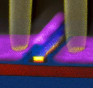
8 Limitation of typical ICP plasmas in terms of selectivity: ion induced damages Typical issue: Si-recess in FDSOI transistors during gate etching PolySi Gate etching in HBr/O 2 plasma PolySi Gate PolySi Gate SiO 2 BOX Thin Oxide gate (1.1 nm) Si channel Si channel BOX Highly selective over SiO 2 oxide gate But H+ and O+ penetration through the oxide gate leads to Si channel oxidation 1.8 nm Today s etching processes are not adapted to ultrathin layers 8

9 The ion/radical synergy: a limitation for atomic precision etching Plasma Cl 2 Cl 2 + e - Cl + d SiClx Masqu e Si SiCl 4 SiO 2 During plasma etching, the surface is bombarded simultaneously and continuously by fluxes of radicals and energetic ions. Incoming ions and neutral species blur the surface forming a thick mixed reactive layer. In this way, energetic ions work in synergy with neutral chemical species from the plasma to remove film from the wafer surface. 9
10 Importance of reactive layer thickness for atomic precision etching Reactive layer Damage of the underneath Si substrate Silicon etching proceeds through the reactive layer propagation Even if the etch selectivity between materials is high, etch precision can be lost if the ion induced mixed layer (reactive layer SiClx layer in this example) is thicker than etch stop layer (thin oxide layer). Damage and etching are convoluted 10

11 Importance of reactive layer thickness for atomic precision etching Reactive layer Damage of the underneath Si substrate Silicon etching proceeds through the reactive layer propagation For atomic precision etching: the reactive layer thickness must be minimized and ideally must be thinner than the etch stop layer thickness Ideal case: Reactive layer thickness = one atomic layer 11


 Experimental conditions: 1 plasma Cl 2 CW Helicon, 300Ws, 4mTorr")

12 Key parameter for controlling the reactive layer : ion energy P. Brichon, E. Despiau-Pujo, J. Appl. Phys. 118, (2015) e SiClx (Å) eV simulation MD exp Layadi et al. 1 exp LTM 2 10eV 25eV 50eV 100eV eV Fluence Cl + = 3, ions/cm 2 Cl/Cl + - Γ n /Γ i = eV 50eV 100eV depth (nm) E ion (ev 1/2 ) Experimental conditions: 1 plasma Cl 2 CW Helicon, 300Ws, 4mTorr 1 Layadi et al., JAP, 81, 6738 (1997) 2 plasma Cl 2 CW-ICP, 600Ws, 5mTorr 2 O. Mourey, thèse en cours au LTM The reactive layer thickness is driven by the ion energy Necessity to work at very low energy to etch ultrathin layers (<25eV) 12


13 Limitation of typical ICP plasmas in terms of CD control and uniformity In conventionnal plasma etching, etch rates and profiles are strongly dependent on the fluxes of reactive species and ions that arrive on the surface A small species gradient will generate local non uniformity such as ARDE or microloading Microloading ARDE Thicker passivation layer Cl Cl Semi isolated Dense Such transport-limited phenomena compromise the atomic precision etching The limitations of current plasma technologies for CD control at the atomic scale originate from the impossibility to control independently of the fluxes of radicals or ion bombarding the surface. 13
14 Outline I. Introduction II. Limitations of current plasma technologies III. Atomic layer etching concept : ALE IV. From lab to fab 14
15 ALE concept* : a way to achieve atomic precision etching ALE is a technique that removes thin layers of material using 2 sequential selflimiting and independent reactions. Surface to be etched Step1: Modification Step 2: Removal End and repeat Self limiting Self limiting Cycle repetition Step 1: Modification forms a thin reactive surface layer with a well defined thickness Self-limited reaction: the formation of the modified layer stops when the surface is saturated with reactants Step 2: The removal step takes away the modified layer while keeping the underlying substrate intact Self-limited reaction: the reaction stops when the modified layer is entierely consummed The surface is resetted to a pristine or near-pristine state for the next etching cycle. *M. N. Yoder, U.S. patent 4,756,794 (12 July 1988). 15


16 ALE offers fundamental advantage for atomic precision The ALE concept allows to overcome the intrinsic limitations of «plasma etching fundamentals» because of: 1. Separation into a sequence of independent unit process reactions 2. Self-limited reactions Consequences on : 1. Surface damage Atomically smooth surface after modification Flat, smooth surface, Same composition after removal 2. Uniformity, CD control, ARDE Identical surface coverage at both the wafer and pattern scale during the modification Same etch depth and profile for any patterns on the wafer 16
17 ALE concept : a way to control independently neutral and ion flux S. D. Athavale,J. Vac. Sci. Technol. B 14, 3702 (1996) A. Agarwal, J. Vac. Sci. Technol A, 27(1), 37 (2009) S-D Park, Jpn J. Appl. Phys. 44, 389 (2005) Step1: Modification Step 2: Removal Cl Ar+ Purge Surface to be etched Two schemes Chemisorption driven by radical O + /O 2 + Removal driven by ionic bombardement Purge End and repeat Conversion: -Oxidation by plasma or wet J. Lin, et al,, IEEE Elec. Dev. Lett., 35, 440,(2014) X. Cao, Microelectron. Eng., 67, 333 (2003). Removal by Wet etching or radicals 17
18 ALE concept : from lab to fab ALE has been studied for over 25 years in laboratory but never implemented into semiconductor high-volume manufacturing because low throughputs and high costefficiency Ex: S-D Park, Jpn J. Appl. Phys. 44, 389 (2005) -ALE of Si with Cl2 thermal adsorption followed by Ar+ ER= 1.36 A/cycle But 1 cycle = 85s (20s chemisorption-20s purge-40s removal-5s purge) 14 min to etch 1nm!! Now that the major industrial concern is ATOMIC PRECISION etching, the ALE concept creates renewed interest How to implement ALE concept with industrial constraints? Which technologies? Develop plasma technologies that allow: Low ion energy (<25eV) An independent control of radical and ion fluxes 1nm in 10s acceptable Low Te plasma reactor Pulsed plasmas Fast injection pulsed plasma Smart etch technology 18
19 Outline I. Introduction II. Limitations of current plasma technologies III. Atomic layer etching concept : ALE IV. From lab to fab 1. Low Te 2. Pulsed plasmas 3. Fast gas injection plasma 4. Smart etch technology 19

20 Low T e plasmas Design a reactor chamber capable to provide electrons with low electronic temperature near the wafer surface (Te <1 ev) Very low ion energy achievable :Vp-Vf~5kTe <5eV How? By separating of the plasma generation region from the wafer plasma region Plasma generation : High Te High n e- Ionization zone: Ar + e- Ar e- Production of secondary e- Wafer Region 1 Region 2 Plasma diffusion: No e- heating by EM wave The secondary electrons cool down through collisions to a very low temperature Low Te (<2 ev) Low Vp < 10eV High n e- An ideal Low Te source has a sufficient ionization population with a reduced dissociation population while maintaining a low bulk Te 20
 Goto et al., Jpn. J. Appl. Phys.")
 Q.")
 Naval research laboratory (NRL) is the first to develop a plasma reactor based on this concept R. A.")
 N5033 (2015) More recently, TEL and AMAT show some interest in this technology.")
21 Several designs RLSA Low T e plasma reactors Electron beam generated plasma Surfacer wave Plasma generated by RLSA antenna* *M. Ando, IEEE Trans. Ant. propag. AP-33, 1347, (1985) Goto et al., Jpn. J. Appl. Phys., 42, 1887 (2003) RLSA technology implemented in industrial plasma reactor in 2010 by TEL C. Tian, J. Vac. Sci. Technol. A 24, 1421, (2006) Q. yang, ECS Transactions, 52 (1) (2013) Concept exists from late 1970 s used for deposition R. A. Dugdale, J. Mat. Sci. 10, 896 (1975) Naval research laboratory (NRL) is the first to develop a plasma reactor based on this concept R. A. Meger,, Large Area Plasma Processing System ( LAPPS) U. S. Pat. 5,874,807 (1999). S.G. Walton et al, ECS J. Of Sol. State Sci.Tech., 4 (6) N5033 (2015) More recently, TEL and AMAT show some interest in this technology. No industrial tool yet L. Chen, PlasmaSources Sci. Technol. 22, (2013). S. Rauf, 61st AVS Int. Symp. and Exhib., Baltimore 21 (2014).
22 Low T e plasma properties Te and Ne in a RLSA reactor Q. yang, ECS Transactions, 52 (1) (2013) Plasma generation Plasma diffusion V p < 5 ev Antenna Wafer Antenna Wafer RLSA can sustain an over-dense high density plasma from a few mtorr to 1torr (ICP<100mT) Te and Ne varies only slightly with chamber pressure Control of N independently of i C. Tian, J. Vac. Sci. Technol. A 24, 1421, (2006) 22
23 Low T e vs ICP summary Design Element ICP Low Te Te 2-4eV < 2 ev Minimum ion energy ev <10 ev VUV flux high low Ion flux Dissociation/Etch byproducts redissociation Ions and radical production high coupled low uncoupled Minimum surface damage Reduced microloading and ARDE 23
24 Outline I. Introduction II. Limitations of current plasma technologies III. Atomic layer etching concept : ALE IV. From lab to fab 1. Low Te 2. Pulsed plasmas 3. Fast gas injection plasma 4. Smart etch technology 24
) In 2009, AMAT commercialized an ICP reactor equipped with Pulsync TM S. Banna, et al., IEEE Trans. Plasma Sci. 37, 1730 (2009).")
25 T T on T off Pulsed plasma technologies Principle: modulation of the plasma power supplies (turned «on» and «off») First studies in the 90 s: source pulsing only Source Power (S. Samukawa,Appl. Phys. Lett (1993)) In 2009, AMAT commercialized an ICP reactor equipped with Pulsync TM S. Banna, et al., IEEE Trans. Plasma Sci. 37, 1730 (2009). Two new knobs: o Frequency: f = 1/T o Duty cycle: DC = T on T on +T off T on T T off Three new regimes: -Source pulsing only -Bias pulsing only -Synchronized pulsing Bias power 25
26 Pulsed plasmas: important timescales For typical etching applications the pulsing frequency is > 1kHz (T<1ms) Ions kinetics Radicals kinetics ion Current (ma.cm -2 ) RF ON 1 khz Ar Cl 2 density (cm -3 ) RF ON 1 khz Ar/Cl Time (ms) Ion production: µs Ion losses (ambipolar diffusion) ~ 100µs 0 0,0 0,2 0,4 0,6 0,8 1,0 Time (ms) Radical production: µs Radical losses (diffusion, pumping)>ms Radical density is not modulated during plasma pulses while ion flux is strongly modulated Pulsing the ICP power allows independent control of the ion flux and radicals flux 26
27 Impact of the duty cycle on the plasma chemistry Cl 2 100sccm, 800Ws, 0 Wb, 20mTorr Decreasing Dissociation Duty cycle is the major knob and controls dissociation Pulsed plasmas with small duty cycle = reduced chemical reactivity Bodart et al., JAP, 110, (2011) 27
28 Impact of the duty cycle on the ion energy distribution CW 75 % 50 % 25 % 10 % Ions from ON period No bias applied to the substrate (in continuous plasma : Ei ~ V p ) RF ON RF OFF Ions from OFF period T e V p 3 ev 15 V T e ~ 0.2 ev V p ~ 1 V Energy (ev) When pulsing the plasma, the ion distribution function switches from unimodal to bimodal During the ON period: the ions are accelerated towards the wafer by V p ~ 15eV (No bias power) Similar behavior for continuous and pulsed plasma During the OFF period: Te and consequently Vp decrease low ion energy (<10eV) By pulsing the plasma, low ion energy regime can be reached 28
29 Impact of the duty cycle on the ion energy distribution CW 75 % 50 % 25 % 10 % Ions from ON period No bias applied to the substrate (in continuous plasma : Ei ~ V p ) RF ON RF OFF Ions from OFF period T e V p 3 ev 15 V T e ~ 0.2 ev V p ~ 1 V Energy (ev) In an ICP plasma pulsed with a small duty cycle the wafer is bombarded by: - Low flux of low energy ions - Low flux of reactive radicals key point to reduce surface damages and local non uniformity 29
 CW b)")


30 Example of application Minimizing Si recess during the over-etch of gate etching processes HBr/O 2 /Ar a) CW b) 5kHz 15% SiO 2 Si poly -Si ~ 2 nm passivation layer poly -Si ~ 1 nm passivation layer ~ 1.5 nm Si recess 1.2 nm gate oxide 1.2 nm gate oxide No recess From Petit-Etienne et al.j. Vac. Sci. Technol B 30(4), 1071 (2012) Minimizing microloading effect during PolySi etching in HBr/O 2 Continuous plasma Pulsed plasma: DC=20%, 1kHz Isolated Dense Isolated Dense Microloading effect M. Haass, J. Vac. Sci. Technol. B 33, (2015) Identical iso-dense profile Better selectivity over HM 30
31 Outline I. Introduction II. Limitations of current plasma technologies III. Atomic layer etching concept : ALE IV. From lab to fab 1. Low Te 2. Pulsed plasmas 3. Fast gas injection plasma 4. Smart etch technology 31
32 How can we reproduce the two steps of the ALE concept in an industrial reactor with acceptable time constraints? Surface to be etched Step1:Modification Cl Purge Step 2:Removal Ar+ Purge End and repeat Chemisorption driven by radical Removal driven by ionic bombardement Step 1: plasma needs to operate in a regime that forms sub-1nm reactive layer Ion energy <25eV Hardly achievable with conventional ICP reactor Can we stop the growth of the reactive layer before it reaches 1 nm thickness? 32

33 A dynamic control of the reactive layer thickness Thickness (nm) Steady state reactive layer Si atom Cl atom 0 ms 100 ms 200 ms 300 ms 400 ms 500 ms Typical time to reach 1nm thick reactive layer ~ ms Sub-1 nm thick reactive layer can be obtained if the reactive gas injection in the plasma chamber is stopped before the reactive layer reaches its steady state thickness Technically feasible by fast gas switching technology (if t >100ms) Patent US B1 (2012) Rapid and uniform gas switching for a plasma etch process 33 33


34 How can we reproduce the two steps of the ALE concept in an industrial reactor with acceptable time constraints? Surface to be etched Step1:Modification Cl Step 2:Removal Ar+ End and repeat Chemisorption driven by radical Removal driven by ionic bombardement Step 2: bombarding particles are used to provide enough energy to break the Si Si bonds that have been weakened by adsorbed chlorine. After 10s plasma for ion flux of 2mA/cm 2 MD simulations show that 25-50eV ion energy range allows -SiCl removal with acceptable time constraint -with limited Si amorphization Paulin Brichon, phd thesis 34


35 Atomic Precision etching using Fast gas injection Reactive layer thickness Step 1 Step 2 Step 1 Step 2 t 1 ~ 100 ms t 2 ~ 10 s Reactive gas injection Ar Cl 2 Ar gas injection e nm 0 nm Time 35
36 Demonstration of Atomic Precision etching using Fast gas injection ICP (Ar/Cl 2 plasma) Plasma enhanced ALE (Cl 2 followed by Ar) Microtrenching Flat etch front Rough Smooth K. J. Kanarik, Solid State Technol. 56, 14 (2013). 36
37 Outline I. Introduction II. Limitations of current plasma technologies III. Atomic layer etching concept : ALE IV. From lab to fab 1. Low Te 2. Pulsed plasmas 3. Fast gas injection plasma 4. Smart etch technology 37
38 Smart etch Technology : An alternative process for thin layer etching Based on the ALE concept using a «conversion» modification step Developped for SiN or SiO 2 materials Surface to be etched H/He ion implantation using ICP or CCP plasma He+/H+ Removal by Wet etching or radicals End and repeat Step 1: Implantation of light ions (He+ or H+) to modify the material without sputtering it The modification depth is driven by ion flux and energy Step 2: Removal of the modified layer by chemical action: Wet etching or radicals produced by downstream plasma The chemical step must present high etch selectivity over the non modified layer N. Posseme, Appl. Phys. Lett. 105, (2014) 38
39 Smart etch Technology: Proof of concept Step 1: Implantation of light ions Impact of ion energy Impact of ion dose (ion flux*time) N. Posseme et al, Appl. Phys. Lett. 105, (2014) The modified layer thickness is driven by the ion energy This step is self-limited: at a given ion energy, the modified layer thickness saturates above a certain ion dose. Respect of the ALE criteria 39


40 Smart etch Technology: Proof of concept Step 2: removal by NF3/NH3 downstream plasma Formation of HF and NH 4 F by NH 3 and NF 3 dissociation and subsequent recombinaison Etching proceeds through the formation of salts that can sublimate for T>100 C SiO2 + 4 HF + 2 NH4F (NH4)2SiF6 (salts) + 2 H2O Etch mechanisms of the modified Si 3 N 4 not well understood However the smart etch technology shows remarkable capability to etch modified Si 3 N 4 layer with excellent selectivity over the non modified Si 3 N 4 After H+ implantation After NH 3 /NF 3 downstream plasma Modified Si3N4 Gate Spacer Si 3 N 4 Almost no consumption of non modified Si 3 N 4 No Si recess Si 40


41 Modified depth (nm) Towards a technological rupture for atomic precision etching AMAT proposes a new reactor design that allows to achieve the two ALE steps in the same chamber 1. Step1: modification by ion implantation generated by CCP plasma Energy (ev) Modification depth driven by ion energy Self limited 41

42 Towards a technological rupture for atomic precision etching AMAT proposes a new reactor design that allows to achieve the two ALE steps in the same chamber 2. Step2 : removal of the modified layer by radicals generated by down stream plasma The etching proceeds through the formation of salts Self limited: the etched amount saturates with process time 42
43 Conclusion The complexification of MOS transistors architecture imposed by the miniaturization requires atomic precision etching CD control at the nanometer scale Etching of ultra thin layers without introducing plasma damage Conventional ICP reactor reach their intrinsic limits to have an atomic precision etching Impossible to control the N / i ratio! Ion energy range is restricted: ev New tool concepts are being introduced to meet the needs of future process technologies The ideal tool does not exist. Each of them have pros and cons. The right tool has to be chosen according to the application targeted 43
44 44
Plasma Etching: Atomic Scale Surface Fidelity and 2D Materials
 1 Plasma Etching: Atomic Scale Surface Fidelity and 2D Materials Thorsten Lill, Keren J. Kanarik, Samantha Tan, Meihua Shen, Alex Yoon, Eric Hudson, Yang Pan, Jeffrey Marks, Vahid Vahedi, Richard A. Gottscho
MODELING OF SEASONING OF REACTORS: EFFECTS OF ION ENERGY DISTRIBUTIONS TO CHAMBER WALLS*
 MODELING OF SEASONING OF REACTORS: EFFECTS OF ION ENERGY DISTRIBUTIONS TO CHAMBER WALLS* Ankur Agarwal a) and Mark J. Kushner b) a) Department of Chemical and Biomolecular Engineering University of Illinois,
ETCHING Chapter 10. Mask. Photoresist
 ETCHING Chapter 10 Mask Light Deposited Substrate Photoresist Etch mask deposition Photoresist application Exposure Development Etching Resist removal Etching of thin films and sometimes the silicon substrate
Patterning Challenges and Opportunities: Etch and Film
 Patterning Challenges and Opportunities: Etch and Film Ying Zhang, Shahid Rauf, Ajay Ahatnagar, David Chu, Amulya Athayde, and Terry Y. Lee Applied Materials, Inc. SEMICON, Taiwan 2016 Sept. 07-09, 2016,
Etching Issues - Anisotropy. Dry Etching. Dry Etching Overview. Etching Issues - Selectivity
 Etching Issues - Anisotropy Dry Etching Dr. Bruce K. Gale Fundamentals of Micromachining BIOEN 6421 EL EN 5221 and 6221 ME EN 5960 and 6960 Isotropic etchants etch at the same rate in every direction mask
DEPOSITION AND COMPOSITION OF POLYMER FILMS IN FLUOROCARBON PLASMAS*
 DEPOSITION AND COMPOSITION OF POLYMER FILMS IN FLUOROCARBON PLASMAS* Kapil Rajaraman and Mark J. Kushner 1406 W. Green St. Urbana, IL 61801 rajaramn@uiuc.edu mjk@uiuc.edu http://uigelz.ece.uiuc.edu November
Fabrication Technology, Part I
 EEL5225: Principles of MEMS Transducers (Fall 2004) Fabrication Technology, Part I Agenda: Microfabrication Overview Basic semiconductor devices Materials Key processes Oxidation Thin-film Deposition Reading:
3.155J/6.152J Microelectronic Processing Technology Fall Term, 2004
 3.155J/6.152J Microelectronic Processing Technology Fall Term, 2004 Bob O'Handley Martin Schmidt Quiz Nov. 17, 2004 Ion implantation, diffusion [15] 1. a) Two identical p-type Si wafers (N a = 10 17 cm
DOE WEB SEMINAR,
 DOE WEB SEMINAR, 2013.03.29 Electron energy distribution function of the plasma in the presence of both capacitive field and inductive field : from electron heating to plasma processing control 1 mm PR
Effect of Noble Gas. Plasma Processing Laboratory University of Houston. Acknowledgements: DoE Plasma Science Center and NSF
 Ion Energy Distributions in Pulsed Plasmas with Synchronous DC Bias: Effect of Noble Gas W. Zhu, H. Shin, V. M. Donnelly and D. J. Economou Plasma Processing Laboratory University of Houston Acknowledgements:
EFFECT OF REACTOR GEOMETRY ON ION ENERGY DISTRIBUTIONS FOR PULSED PLASMA DOPING (P 2 LAD)*
*") EFFECT OF REACTOR GEOMETRY ON ION ENERGY DISTRIBUTIONS FOR PULSED PLASMA DOPING (P 2 LAD)* Ankur Agarwal a) and Mark J. Kushner b) a) Department of Chemical and Biomolecular Engineering University of Illinois
EFFECT OF REACTOR GEOMETRY ON ION ENERGY DISTRIBUTIONS FOR PULSED PLASMA DOPING (P 2 LAD)* Ankur Agarwal a) and Mark J. Kushner b) a) Department of Chemical and Biomolecular Engineering University of Illinois
P. Diomede, D. J. Economou and V. M. Donnelly Plasma Processing Laboratory, University of Houston
 P. Diomede, D. J. Economou and V. M. Donnelly Plasma Processing Laboratory, University of Houston 1 Outline Introduction PIC-MCC simulation of tailored bias on boundary electrode Semi-analytic model Comparison
Plasma Deposition (Overview) Lecture 1
 Lecture 1") Plasma Deposition (Overview) Lecture 1 Material Processes Plasma Processing Plasma-assisted Deposition Implantation Surface Modification Development of Plasma-based processing Microelectronics needs (fabrication
Plasma Deposition (Overview) Lecture 1 Material Processes Plasma Processing Plasma-assisted Deposition Implantation Surface Modification Development of Plasma-based processing Microelectronics needs (fabrication
CVD: General considerations.
 CVD: General considerations. PVD: Move material from bulk to thin film form. Limited primarily to metals or simple materials. Limited by thermal stability/vapor pressure considerations. Typically requires
Hong Young Chang Department of Physics, Korea Advanced Institute of Science and Technology (KAIST), Republic of Korea
, Republic of Korea") Hong Young Chang Department of Physics, Korea Advanced Institute of Science and Technology (KAIST), Republic of Korea Index 1. Introduction 2. Some plasma sources 3. Related issues 4. Summary -2 Why is
Hong Young Chang Department of Physics, Korea Advanced Institute of Science and Technology (KAIST), Republic of Korea Index 1. Introduction 2. Some plasma sources 3. Related issues 4. Summary -2 Why is
A global (volume averaged) model of a chlorine discharge
 model of a chlorine discharge") A global (volume averaged) model of a chlorine discharge Eyþór Gísli Þorsteinsson and Jón Tómas Guðmundsson Science Institute, University of Iceland, Iceland Department of Electrical and Computer Engineering,
A global (volume averaged) model of a chlorine discharge Eyþór Gísli Þorsteinsson and Jón Tómas Guðmundsson Science Institute, University of Iceland, Iceland Department of Electrical and Computer Engineering,
Etching: Basic Terminology
 Lecture 7 Etching Etching: Basic Terminology Introduction : Etching of thin films and sometimes the silicon substrate are very common process steps. Usually selectivity, and directionality are the first
INVESTIGATION of Si and SiO 2 ETCH MECHANISMS USING an INTEGRATED SURFACE KINETICS MODEL
 46 th AVS International Symposium Oct. 25-29, 1999 Seattle, WA INVESTIGATION of Si and SiO 2 ETCH MECHANISMS USING an INTEGRATED SURFACE KINETICS MODEL Da Zhang* and Mark J. Kushner** *Department of Materials
CHAPTER 6: Etching. Chapter 6 1
 Chapter 6 1 CHAPTER 6: Etching Different etching processes are selected depending upon the particular material to be removed. As shown in Figure 6.1, wet chemical processes result in isotropic etching
4FNJDPOEVDUPS 'BCSJDBUJPO &UDI
 2010.5.4 1 Major Fabrication Steps in CMOS Process Flow UV light oxygen Silicon dioxide Silicon substrate Oxidation (Field oxide) photoresist Photoresist Coating Mask exposed photoresist Mask-Wafer Exposed
The effect of the chamber wall on fluorocarbonassisted atomic layer etching of SiO 2 using cyclic Ar/C 4 F 8 plasma
 The effect of the chamber wall on fluorocarbonassisted atomic layer etching of SiO 2 using cyclic Ar/C 4 F 8 plasma Running title: The effect of the chamber wall on FC assisted atomic layer etching of
Plasma atomic layer etching using conventional plasma equipment
 Plasma atomic layer etching using conventional plasma equipment Ankur Agarwal a Department of Chemical and Biomolecular Engineering, University of Illinois, 600 S. Mathews Ave., Urbana, Illinois 61801
Reactive Ion Etching (RIE)
") Reactive Ion Etching (RIE) RF 13.56 ~ MHz plasma Parallel-Plate Reactor wafers Sputtering Plasma generates (1) Ions (2) Activated neutrals Enhance chemical reaction 1 2 Remote Plasma Reactors Plasma Sources
Reactive Ion Etching (RIE) RF 13.56 ~ MHz plasma Parallel-Plate Reactor wafers Sputtering Plasma generates (1) Ions (2) Activated neutrals Enhance chemical reaction 1 2 Remote Plasma Reactors Plasma Sources
Lecture 6 Plasmas. Chapters 10 &16 Wolf and Tauber. ECE611 / CHE611 Electronic Materials Processing Fall John Labram 1/68
 Lecture 6 Plasmas Chapters 10 &16 Wolf and Tauber 1/68 Announcements Homework: Homework will be returned to you on Thursday (12 th October). Solutions will be also posted online on Thursday (12 th October)
LECTURE 5 SUMMARY OF KEY IDEAS
 LECTURE 5 SUMMARY OF KEY IDEAS Etching is a processing step following lithography: it transfers a circuit image from the photoresist to materials form which devices are made or to hard masking or sacrificial
PIC-MCC/Fluid Hybrid Model for Low Pressure Capacitively Coupled O 2 Plasma
 PIC-MCC/Fluid Hybrid Model for Low Pressure Capacitively Coupled O 2 Plasma Kallol Bera a, Shahid Rauf a and Ken Collins a a Applied Materials, Inc. 974 E. Arques Ave., M/S 81517, Sunnyvale, CA 9485, USA
Robert A. Meger Richard F. Fernster Martin Lampe W. M. Manheimer NOTICE
 Serial Number Filing Date Inventor 917.963 27 August 1997 Robert A. Meger Richard F. Fernster Martin Lampe W. M. Manheimer NOTICE The above identified patent application is available for licensing. Requests
PIC-MCC/Fluid Hybrid Model for Low Pressure Capacitively Coupled O 2 Plasma
 PIC-MCC/Fluid Hybrid Model for Low Pressure Capacitively Coupled O 2 Plasma Kallol Bera a, Shahid Rauf a and Ken Collins a a Applied Materials, Inc. 974 E. Arques Ave., M/S 81517, Sunnyvale, CA 9485, USA
Plasma-Surface Interactions in Patterning High-k k Dielectric Materials
 Plasma-Surface Interactions in Patterning High-k k Dielectric Materials October 11, 4 Feature Level Compensation and Control Seminar Jane P. Chang Department of Chemical Engineering University of California,
EFFECT OF PRESSURE AND ELECTRODE SEPARATION ON PLASMA UNIFORMITY IN DUAL FREQUENCY CAPACITIVELY COUPLED PLASMA TOOLS *
 EFFECT OF PRESSURE AND ELECTRODE SEPARATION ON PLASMA UNIFORMITY IN DUAL FREQUENCY CAPACITIVELY COUPLED PLASMA TOOLS * Yang Yang a) and Mark J. Kushner b) a) Department of Electrical and Computer Engineering
Normally-Off GaN Field Effect Power Transistors: Device Design and Process Technology Development
 Center for High Performance Power Electronics Normally-Off GaN Field Effect Power Transistors: Device Design and Process Technology Development Dr. Wu Lu (614-292-3462, lu.173@osu.edu) Dr. Siddharth Rajan
Control of Ion Energy Distributions on Plasma Electrodes
 Control of Ion Energy Distributions on Plasma Electrodes P. Diomede, D. J. Economou and V. M. Donnelly Plasma Processing Laboratory, University of Houston DOE Plasma Science Center Teleseminar, February
H. Shin, W. Zhu, V. M. Donnelly, and D. J. Economou University of Houston. November 2, AVS 58h International Symposium, Nashville, TN, USA
 Near-Threshold Ion-Enhanced Silicon Etching H. Shin, W. Zhu, V. M. Donnelly, and D. J. Economou o ou University of Houston Acknowledgements: DOE Plasma Science Center, NSF and Varian Semiconductor Equipment
MOSFET: Introduction
 E&CE 437 Integrated VLSI Systems MOS Transistor 1 of 30 MOSFET: Introduction Metal oxide semiconductor field effect transistor (MOSFET) or MOS is widely used for implementing digital designs Its major
Plasma Chemistry Study in an Inductively Coupled Dielectric Etcher
 Plasma Chemistry Study in an Inductively Coupled Dielectric Etcher Chunshi Cui, John Trow, Ken Collins, Betty Tang, Luke Zhang, Steve Shannon, and Yan Ye Applied Materials, Inc. October 26, 2000 10/28/2008
EE 527 MICROFABRICATION. Lecture 24 Tai-Chang Chen University of Washington
 EE 527 MICROFABRICATION Lecture 24 Tai-Chang Chen University of Washington EDP ETCHING OF SILICON - 1 Ethylene Diamine Pyrocatechol Anisotropy: (100):(111) ~ 35:1 EDP is very corrosive, very carcinogenic,
Lecture 04 Review of MOSFET
 ECE 541/ME 541 Microelectronic Fabrication Techniques Lecture 04 Review of MOSFET Zheng Yang (ERF 3017, email: yangzhen@uic.edu) What is a Transistor? A Switch! An MOS Transistor V GS V T V GS S Ron D
MODELING OF AN ECR SOURCE FOR MATERIALS PROCESSING USING A TWO DIMENSIONAL HYBRID PLASMA EQUIPMENT MODEL. Ron L. Kinder and Mark J.
 TECHCON 98 Las Vegas, Nevada September 9-11, 1998 MODELING OF AN ECR SOURCE FOR MATERIALS PROCESSING USING A TWO DIMENSIONAL HYBRID PLASMA EQUIPMENT MODEL Ron L. Kinder and Mark J. Kushner Department of
PLASMA immersion ion implantation (PIII) is a fledgling
 is a fledgling") IEEE TRANSACTIONS ON PLASMA SCIENCE, VOL. 26, NO. 6, DECEMBER 1998 1661 Low Pressure Plasma Immersion Ion Implantation of Silicon Zhi-Neng Fan, Qing-Chuan Chen, Paul K. Chu, Member, IEEE, and Chung Chan
IEEE TRANSACTIONS ON PLASMA SCIENCE, VOL. 26, NO. 6, DECEMBER 1998 1661 Low Pressure Plasma Immersion Ion Implantation of Silicon Zhi-Neng Fan, Qing-Chuan Chen, Paul K. Chu, Member, IEEE, and Chung Chan
Physique des plasmas radiofréquence Pascal Chabert
 Physique des plasmas radiofréquence Pascal Chabert LPP, Ecole Polytechnique pascal.chabert@lpp.polytechnique.fr Planning trois cours : Lundi 30 Janvier: Rappels de physique des plasmas froids Lundi 6 Février:
Section 12: Intro to Devices
 Section 12: Intro to Devices Extensive reading materials on reserve, including Robert F. Pierret, Semiconductor Device Fundamentals EE143 Ali Javey Bond Model of Electrons and Holes Si Si Si Si Si Si Si
Wet and Dry Etching. Theory
 Wet and Dry Etching Theory 1. Introduction Etching techniques are commonly used in the fabrication processes of semiconductor devices to remove selected layers for the purposes of pattern transfer, wafer
Section 3: Etching. Jaeger Chapter 2 Reader
 Section 3: Etching Jaeger Chapter 2 Reader Etch rate Etch Process - Figures of Merit Etch rate uniformity Selectivity Anisotropy d m Bias and anisotropy etching mask h f substrate d f d m substrate d f
Feature-level Compensation & Control
 Feature-level Compensation & Control 2 Plasma Eray Aydil, UCSB, Mike Lieberman, UCB and David Graves UCB Workshop November 19, 2003 Berkeley, CA 3 Feature Profile Evolution Simulation Eray S. Aydil University
MICROCHIP MANUFACTURING by S. Wolf
 by S. Wolf Chapter 15 ALUMINUM THIN-FILMS and SPUTTER-DEPOSITION 2004 by LATTICE PRESS CHAPTER 15 - CONTENTS Aluminum Thin-Films Sputter-Deposition Process Steps Physics of Sputter-Deposition Magnetron-Sputtering
Etching Applications and Discoveries Made Possible by Advanced Ion Energy Control
 Etching Applications and Discoveries Made Possible by Advanced Ion Energy Control Possible by Advanced Ion Energy Control V. M. Donnelly Department of Chemical and Biomolecular Engineering University of
Chapter 6. Summary and Conclusions
 Chapter 6 Summary and Conclusions Plasma deposited amorphous hydrogenated carbon films (a-c:h) still attract a lot of interest due to their extraordinary properties. Depending on the deposition conditions
an introduction to Semiconductor Devices
 an introduction to Semiconductor Devices Donald A. Neamen Chapter 6 Fundamentals of the Metal-Oxide-Semiconductor Field-Effect Transistor Introduction: Chapter 6 1. MOSFET Structure 2. MOS Capacitor -
Plasma Processing in the Microelectronics Industry. Bert Ellingboe Plasma Research Laboratory
 Plasma Processing in the Microelectronics Industry Bert Ellingboe Plasma Research Laboratory Outline What has changed in the last 12 years? What is the relavant plasma physics? Sheath formation Sheath
Chapter 7 Plasma Basic
 Chapter 7 Plasma Basic Hong Xiao, Ph. D. hxiao89@hotmail.com www2.austin.cc.tx.us/hongxiao/book.htm Hong Xiao, Ph. D. www2.austin.cc.tx.us/hongxiao/book.htm 1 Objectives List at least three IC processes
Stretching the Barriers An analysis of MOSFET Scaling. Presenters (in order) Zeinab Mousavi Stephanie Teich-McGoldrick Aseem Jain Jaspreet Wadhwa
 Zeinab Mousavi Stephanie Teich-McGoldrick Aseem Jain Jaspreet Wadhwa") Stretching the Barriers An analysis of MOSFET Scaling Presenters (in order) Zeinab Mousavi Stephanie Teich-McGoldrick Aseem Jain Jaspreet Wadhwa Why Small? Higher Current Lower Gate Capacitance Higher
Stretching the Barriers An analysis of MOSFET Scaling Presenters (in order) Zeinab Mousavi Stephanie Teich-McGoldrick Aseem Jain Jaspreet Wadhwa Why Small? Higher Current Lower Gate Capacitance Higher
Section 12: Intro to Devices
 Section 12: Intro to Devices Extensive reading materials on reserve, including Robert F. Pierret, Semiconductor Device Fundamentals Bond Model of Electrons and Holes Si Si Si Si Si Si Si Si Si Silicon
Lecture 150 Basic IC Processes (10/10/01) Page ECE Analog Integrated Circuits and Systems P.E. Allen
 Page ECE Analog Integrated Circuits and Systems P.E. Allen") Lecture 150 Basic IC Processes (10/10/01) Page 1501 LECTURE 150 BASIC IC PROCESSES (READING: TextSec. 2.2) INTRODUCTION Objective The objective of this presentation is: 1.) Introduce the fabrication of
Lecture 150 Basic IC Processes (10/10/01) Page 1501 LECTURE 150 BASIC IC PROCESSES (READING: TextSec. 2.2) INTRODUCTION Objective The objective of this presentation is: 1.) Introduce the fabrication of
Shapes of agglomerates in plasma etching reactors
 Shapes of agglomerates in plasma etching reactors Fred Y. Huang a) and Mark J. Kushner b) University of Illinois, Department of Electrical and Computer Engineering, 1406 West Green Street, Urbana, Illinois
SPUTTER-WIND HEATING IN IONIZED METAL PVD+
 SPUTTER-WIND HEATING IN IONIZED METAL PVD+ Junqing Lu* and Mark Kushner** *Department of Mechanical and Industrial Engineering **Department of Electrical and Computer Engineering University of Illinois
Chemical Vapor Deposition (CVD)
") Chemical Vapor Deposition (CVD) source chemical reaction film substrate More conformal deposition vs. PVD t Shown here is 100% conformal deposition ( higher temp has higher surface diffusion) t step 1
Chemical Vapor Deposition (CVD) source chemical reaction film substrate More conformal deposition vs. PVD t Shown here is 100% conformal deposition ( higher temp has higher surface diffusion) t step 1
In situ electrical characterization of dielectric thin films directly exposed to plasma vacuum-ultraviolet radiation
 JOURNAL OF APPLIED PHYSICS VOLUME 88, NUMBER 4 15 AUGUST 2000 In situ electrical characterization of dielectric thin films directly exposed to plasma vacuum-ultraviolet radiation C. Cismaru a) and J. L.
EE 527 MICROFABRICATION. Lecture 25 Tai-Chang Chen University of Washington
 EE 527 MICROFABRICATION Lecture 25 Tai-Chang Chen University of Washington ION MILLING SYSTEM Kaufmann source Use e-beam to strike plasma A magnetic field applied to increase ion density Drawback Low etch
Plasma Technology September 15, 2005 A UC Discovery Project
 1 Feature-level Compensation & Control Plasma Technology September 15, 2005 A UC Discovery Project 9/15/05 - Plasma Technology 2 Plasma Technology Professors Jane P. Chang (UCLA), Michael A. Lieberman,
CMOS Scaling. Two motivations to scale down. Faster transistors, both digital and analog. To pack more functionality per area. Lower the cost!
 Two motivations to scale down CMOS Scaling Faster transistors, both digital and analog To pack more functionality per area. Lower the cost! (which makes (some) physical sense) Scale all dimensions and
Capacitance-Voltage characteristics of nanowire trigate MOSFET considering wave functionpenetration
 Global Journal of researches in engineering Electrical and electronics engineering Volume 12 Issue 2 Version 1.0 February 2012 Type: Double Blind Peer Reviewed International Research Journal Publisher:
Quantum Mechanical Simulation for Ultra-thin High-k Gate Dielectrics Metal Oxide Semiconductor Field Effect Transistors
 Mechanical Simulation for Ultra-thin High-k Gate Dielectrics Metal Oxide Semiconductor Field Effect Transistors Shih-Ching Lo 1, Yiming Li 2,3, and Jyun-Hwei Tsai 1 1 National Center for High-Performance
DEPOSITION OF THIN TiO 2 FILMS BY DC MAGNETRON SPUTTERING METHOD
 Chapter 4 DEPOSITION OF THIN TiO 2 FILMS BY DC MAGNETRON SPUTTERING METHOD 4.1 INTRODUCTION Sputter deposition process is another old technique being used in modern semiconductor industries. Sputtering
L ECE 4211 UConn F. Jain Scaling Laws for NanoFETs Chapter 10 Logic Gate Scaling
 L13 04202017 ECE 4211 UConn F. Jain Scaling Laws for NanoFETs Chapter 10 Logic Gate Scaling Scaling laws: Generalized scaling (GS) p. 610 Design steps p.613 Nanotransistor issues (page 626) Degradation
Numerical Simulation: Effects of Gas Flow and Rf Current Direction on Plasma Uniformity in an ICP Dry Etcher
 Appl. Sci. Converg. Technol. 26(6): 189-194 (2017) http://dx.doi.org/10.5757/asct.2017.26.6.189 Research Paper Numerical Simulation: Effects of Gas Flow and Rf Current Direction on Plasma Uniformity in
Lecture 8. Detectors for Ionizing Particles
 Lecture 8 Detectors for Ionizing Particles Content Introduction Overview of detector systems Sources of radiation Radioactive decay Cosmic Radiation Accelerators Interaction of Radiation with Matter General
Chapter 7. Plasma Basics
 Chapter 7 Plasma Basics 2006/4/12 1 Objectives List at least three IC processes using plasma Name three important collisions in plasma Describe mean free path Explain how plasma enhance etch and CVD processes
Evaluation of the plasmaless gaseous etching process
 Solid State Phenomena Vol. 134 (28) pp 7-1 Online available since 27/Nov/2 at www.scientific.net (28) Trans Tech Publications, Switzerland doi:1.428/www.scientific.net/ssp.134.7 Evaluation of the plasmaless
SIMULATIONS OF ECR PROCESSING SYSTEMS SUSTAINED BY AZIMUTHAL MICROWAVE TE(0,n) MODES*
 MODES*") 25th IEEE International Conference on Plasma Science Raleigh, North Carolina June 1-4, 1998 SIMULATIONS OF ECR PROCESSING SYSTEMS SUSTAINED BY AZIMUTHAL MICROWAVE TE(,n) MODES* Ron L. Kinder and Mark J.
25th IEEE International Conference on Plasma Science Raleigh, North Carolina June 1-4, 1998 SIMULATIONS OF ECR PROCESSING SYSTEMS SUSTAINED BY AZIMUTHAL MICROWAVE TE(,n) MODES* Ron L. Kinder and Mark J.
E SC 412 Nanotechnology: Materials, Infrastructure, and Safety Wook Jun Nam
 E SC 412 Nanotechnology: Materials, Infrastructure, and Safety Wook Jun Nam Lecture 10 Outline 1. Wet Etching/Vapor Phase Etching 2. Dry Etching DC/RF Plasma Plasma Reactors Materials/Gases Etching Parameters
Plasma etching. Bibliography
 Plasma etching Bibliography 1. B. Chapman, Glow discharge processes, (Wiley, New York, 1980). - Classical plasma processing of etching and sputtering 2. D. M. Manos and D. L. Flamm, Plasma etching; An
Chapter 2 On-wafer UV Sensor and Prediction of UV Irradiation Damage
 Chapter 2 On-wafer UV Sensor and Prediction of UV Irradiation Damage Abstract UV radiation during plasma processing affects the surface of materials. Nevertheless, the interaction of UV photons with surface
Self-study problems and questions Processing and Device Technology, FFF110/FYSD13
 Self-study problems and questions Processing and Device Technology, FFF110/FYSD13 Version 2016_01 In addition to the problems discussed at the seminars and at the lectures, you can use this set of problems
Film Deposition Part 1
 1 Film Deposition Part 1 Chapter 11 : Semiconductor Manufacturing Technology by M. Quirk & J. Serda Spring Semester 2013 Saroj Kumar Patra Semidonductor Manufacturing Technology, Norwegian University of
PRINCIPLES OF PLASMA DISCHARGES AND MATERIALS PROCESSING
 PRINCIPLES OF PLASMA DISCHARGES AND MATERIALS PROCESSING Second Edition MICHAEL A. LIEBERMAN ALLAN J, LICHTENBERG WILEY- INTERSCIENCE A JOHN WILEY & SONS, INC PUBLICATION CONTENTS PREFACE xrrii PREFACE
FLCC Seminar. Spacer Lithography for Reduced Variability in MOSFET Performance
 1 Seminar Spacer Lithography for Reduced Variability in MOSFET Performance Prof. Tsu-Jae King Liu Electrical Engineering & Computer Sciences Dept. University of California at Berkeley Graduate Student:
EE130: Integrated Circuit Devices
 EE130: Integrated Circuit Devices (online at http://webcast.berkeley.edu) Instructor: Prof. Tsu-Jae King (tking@eecs.berkeley.edu) TA s: Marie Eyoum (meyoum@eecs.berkeley.edu) Alvaro Padilla (apadilla@eecs.berkeley.edu)
UHF-ECR Plasma Etching System for Dielectric Films of Next-generation Semiconductor Devices
 UHF-ECR Plasma Etching System for Dielectric Films of Next-generation Semiconductor Devices 1 UHF-ECR Plasma Etching System for Dielectric Films of Next-generation Semiconductor Devices Katsuya Watanabe
nmos IC Design Report Module: EEE 112
 nmos IC Design Report Author: 1302509 Zhao Ruimin Module: EEE 112 Lecturer: Date: Dr.Zhao Ce Zhou June/5/2015 Abstract This lab intended to train the experimental skills of the layout designing of the
I. INTRODUCTION. 127 J. Vac. Sci. Technol. B 15(1), Jan/Feb X/97/15(1)/127/6/$ American Vacuum Society 127
, Jan/Feb X/97/15(1)/127/6/$ American Vacuum Society 127") Real-time process sensing and metrology in amorphous and selective area silicon plasma enhanced chemical vapor deposition using in situ mass spectrometry Ashfaqul I. Chowdhury, a) Walter W. Read, a) Gary
Real-time process sensing and metrology in amorphous and selective area silicon plasma enhanced chemical vapor deposition using in situ mass spectrometry Ashfaqul I. Chowdhury, a) Walter W. Read, a) Gary
Hotwire-assisted Atomic Layer Deposition of Pure Metals and Metal Nitrides
 Hotwire-assisted Atomic Layer Deposition of Pure Metals and Metal Nitrides Alexey Kovalgin MESA+ Institute for Nanotechnology Semiconductor Components group a.y.kovalgin@utwente.nl 1 Motivation 1. Materials
Fundamentals of the Metal Oxide Semiconductor Field-Effect Transistor
 Triode Working FET Fundamentals of the Metal Oxide Semiconductor Field-Effect Transistor The characteristics of energy bands as a function of applied voltage. Surface inversion. The expression for the
ELEN0037 Microelectronic IC Design. Prof. Dr. Michael Kraft
 ELEN0037 Microelectronic IC Design Prof. Dr. Michael Kraft Lecture 2: Technological Aspects Technology Passive components Active components CMOS Process Basic Layout Scaling CMOS Technology Integrated
INTRODUCTION TO THE HYBRID PLASMA EQUIPMENT MODEL
 INTRODUCTION TO THE HYBRID PLASMA EQUIPMENT MODEL Prof. Mark J. Kushner Department of Electrical and Computer Engineering 1406 W. Green St. Urbana, IL 61801 217-144-5137 mjk@uiuc.edu http://uigelz.ece.uiuc.edu
Microelectronics Part 1: Main CMOS circuits design rules
 GBM8320 Dispositifs Médicaux telligents Microelectronics Part 1: Main CMOS circuits design rules Mohamad Sawan et al. Laboratoire de neurotechnologies Polystim! http://www.cours.polymtl.ca/gbm8320/! med-amine.miled@polymtl.ca!
K. Takechi a) and M. A. Lieberman Department of Electrical Engineering and Computer Sciences, University of California, Berkeley, California 94720
 and M. A. Lieberman Department of Electrical Engineering and Computer Sciences, University of California, Berkeley, California 94720") JOURNAL OF APPLIED PHYSICS VOLUME 90, NUMBER 7 1 OCTOBER 2001 Effect of Ar addition to an O 2 plasma in an inductively coupled, traveling wave driven, large area plasma source: O 2 ÕAr mixture plasma modeling
JOURNAL OF APPLIED PHYSICS VOLUME 90, NUMBER 7 1 OCTOBER 2001 Effect of Ar addition to an O 2 plasma in an inductively coupled, traveling wave driven, large area plasma source: O 2 ÕAr mixture plasma modeling
Introduction to Thin Film Processing
 Introduction to Thin Film Processing Deposition Methods Many diverse techniques available Typically based on three different methods for providing a flux of atomic or molecular material Evaporation Sputtering
ESE 570: Digital Integrated Circuits and VLSI Fundamentals
 ESE 570: Digital Integrated Circuits and VLSI Fundamentals Lec 4: January 23, 2018 MOS Transistor Theory, MOS Model Penn ESE 570 Spring 2018 Khanna Lecture Outline! CMOS Process Enhancements! Semiconductor
Nanopantography: A method for parallel writing of etched and deposited nanopatterns
 Nanopantography: A method for parallel writing of etched and deposited nanopatterns Vincent M. Donnelly 1, Lin Xu 1, Azeem Nasrullah 2, Zhiying Chen 1, Sri C. Vemula 2, Manish Jain 1, Demetre J. Economou
EE143 Fall 2016 Microfabrication Technologies. Lecture 6: Thin Film Deposition Reading: Jaeger Chapter 6
 EE143 Fall 2016 Microfabrication Technologies Lecture 6: Thin Film Deposition Reading: Jaeger Chapter 6 Prof. Ming C. Wu wu@eecs.berkeley.edu 511 Sutardja Dai Hall (SDH) 1 Vacuum Basics Units 1 atmosphere
Metal Deposition. Filament Evaporation E-beam Evaporation Sputter Deposition
 Metal Deposition Filament Evaporation E-beam Evaporation Sputter Deposition 1 Filament evaporation metals are raised to their melting point by resistive heating under vacuum metal pellets are placed on
Scaling Issues in Planar FET: Dual Gate FET and FinFETs
 Scaling Issues in Planar FET: Dual Gate FET and FinFETs Lecture 12 Dr. Amr Bayoumi Fall 2014 Advanced Devices (EC760) Arab Academy for Science and Technology - Cairo 1 Outline Scaling Issues for Planar
High-Precision Evaluation of Ultra-Shallow Impurity Profiles by Secondary Ion Mass Spectrometry
 High-Precision Evaluation of Ultra-Shallow Impurity Profiles by Secondary Ion Mass Spectrometry Yoko Tada Kunihiro Suzuki Yuji Kataoka (Manuscript received December 28, 2009) As complementary metal oxide
Part 5: Quantum Effects in MOS Devices
 Quantum Effects Lead to Phenomena such as: Ultra Thin Oxides Observe: High Leakage Currents Through the Oxide - Tunneling Depletion in Poly-Si metal gate capacitance effect Thickness of Inversion Layer
Dry Etching Zheng Yang ERF 3017, MW 5:15-6:00 pm
 Dry Etching Zheng Yang ERF 3017, email: yangzhen@uic.edu, MW 5:15-6:00 pm Page 1 Page 2 Dry Etching Why dry etching? - WE is limited to pattern sizes above 3mm - WE is isotropic causing underetching -
Graphene devices and integration: A primer on challenges
 Graphene devices and integration: A primer on challenges Archana Venugopal (TI) 8 Nov 2016 Acknowledgments: Luigi Colombo (TI) UT Dallas and UT Austin 1 Outline Where we are Issues o Contact resistance
ABSTRACT COMPARISON OF ADVANCED RESIST ETCHING IN E-BEAM GENERATED PLASMAS
 ABSTRACT Title: COMPARISON OF ADVANCED RESIST ETCHING IN E-BEAM GENERATED PLASMAS Bryan J. Orf, Masters of Science, 2006 Directed By: Professor Gottlieb S. Oehrlein, Department of Material Science and
UNIVERSITY OF CALIFORNIA College of Engineering Department of Electrical Engineering and Computer Sciences. Fall Exam 1
 UNIVERSITY OF CALIFORNIA College of Engineering Department of Electrical Engineering and Computer Sciences EECS 143 Fall 2008 Exam 1 Professor Ali Javey Answer Key Name: SID: 1337 Closed book. One sheet
EE410 vs. Advanced CMOS Structures
 EE410 vs. Advanced CMOS Structures Prof. Krishna S Department of Electrical Engineering S 1 EE410 CMOS Structure P + poly-si N + poly-si Al/Si alloy LPCVD PSG P + P + N + N + PMOS N-substrate NMOS P-well
Ion Implantation. alternative to diffusion for the introduction of dopants essentially a physical process, rather than chemical advantages:
 Ion Implantation alternative to diffusion for the introduction of dopants essentially a physical process, rather than chemical advantages: mass separation allows wide varies of dopants dose control: diffusion