FRAUNHOFER IISB STRUCTURE SIMULATION
|
|
|
- Howard Austin
- 6 years ago
- Views:
Transcription
1 FRAUNHOFER IISB STRUCTURE SIMULATION Eberhard Bär Page 1
2 FRAUNHOFER IISB STRUCTURE SIMULATION Overview SiO 2 etching in a C 2 F 6 plasma Ga ion beam sputter etching Ionized metal plasma (IMP) deposition Oxide deposition processes Superconformal copper deposition Coupled simulation of deposition and etching Stressed AlSiCu interconnect line Hierarchical modeling of coils consisting of litz wires Potential distribution in copper-ceramics substrate Coupling of topography simulation and electrical extraction Page 2
3 Structure Simulation Overview Simulation of various structures Microelectronic devices or interconnects Semiconductor manufacturing equipment Macroscopic structures, e.g., for power electronic applications Software integration E.g., TCAD suites, electrical, thermal and mechanical modeling with FEM software such as ANSYS Modeling of structure evolution for microelectronic applications Etching, deposition, CMP Modeling of structures under operation Electrical, thermal, mechanical behavior Reliability of passive components, e.g. due to electromigration Page 3

4 Simulation of SiO 2 Etching in C 2 F 6 Plasma Influence of Equipment Parameters on Feature Profile Neutral flux j neut,0 at surface Ion flux j ion,0 at surface Neutral flux j neut,0 at surface Ion flux 5*j ion,0 at surface Page 4
 image) Monte Carlo Simulation x (microns)")
5 Simulation of Ga Ion Beam Sputter Etching z (microns) Comparison between simulation and experiment (grey region: data obtained from scanning electron microscopy (SEM) image) Monte Carlo Simulation x (microns) Page 5

6 Simulation of Ionized Metal Plasma (IMP) Deposition Influence of Bias Bias = 20 V => resputtering 0 Bias = 100 V => resputtering 0.4 Sticking coefficient of metal atoms and metal ions = 1 Isotropic angular distribution of metal atoms Bias = 20 V Bias = 100 V Page 6

7 Simulation of Low-Temperature Oxide Deposition for the Formation of Air Gap Dielectrics Simulation for precursor sticking coefficient = 0.4 Data: EU project PULLNANO Page 7
8 Simulation of Plasma-Enhanced Chemical Vapor Deposition (PECVD) of Oxide Model: Rate contributions are due to Neutrals (radicals): isotropic angular distribution Ions: Gaussian distribution Local rate R PECVD ~ ( s c F neutral + F ion ), with F: local particle flux, s c : neutral sticking coefficient Model parameters: r = R neutral / ( R neutral + R ion ) in 1D regions, sticking coefficient of neutrals s c, of Gaussian distribution for ions Implementation F neutral from model which determines adsorption and re-emission of reactive molecules or radicals, F ion from flux integration of the ions Page 8
 Ions (O")
 in a CCP")
9 PECVD of SiO 2 with TEOS Chemistry Oxygen Plasma Simulation with Quantemol Q-VT Neutrals (O) Ions (O 2 +) Example for concentration of neutrals (O) and ions (dominant ion species is O 2 +) in a CCP reactor Page 9


10 PECVD of SiO 2 with TEOS Chemistry Feature-Scale Model with Ion Support for Deposition SiO 2 layer deposited in hole position at 0.0 cm position at 10.0 cm Page 10
11 Simulation of Superconformal Copper Deposition Simulation of deposition into trench and via under identical conditions (agreement with experimental data for superconformal CVD) Trench Via Page 11
12 Simulation of Plasma-Enhanced CVD (PECVD) Simulation for two trenches with different aspect ratios Model parameters: r = R neutral / ( R neutral + R ion ) = 1 s c = 0.18 Page 12
13 Influence of Ion Energy on Profile after Back Etching Simulated profiles after sputter etching for different energies of the Ar ions (upper curve: 250 ev, middle curve: 200 ev, lower curve: 180 ev) Page 13

14 Comparison of Simulation and Experiment Data: FhG IMS, Duisburg Simulation (for Ar ion energy = 250 ev) of sputter etching in comparison to the experimental data, good agreement for both trenches is obtained Page 14
15 Modeling of Stressed AlSiCu Interconnect Line Vacancy concentration in interconnect line as criterion for time-tofailure to allow comparison to experimental data w L Example for simulated vacancy distribution c v along metal line under current and thermal stress Page 15
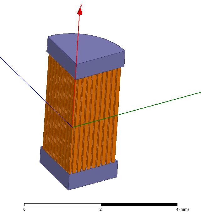
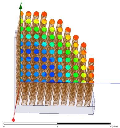
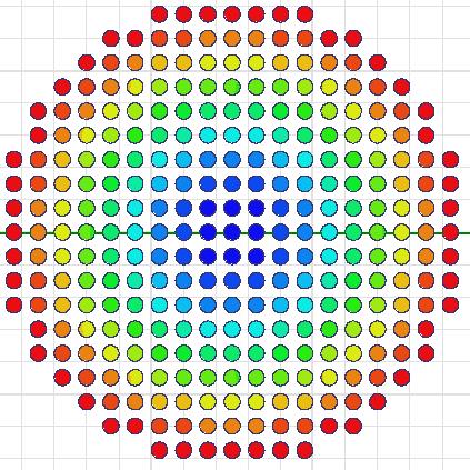
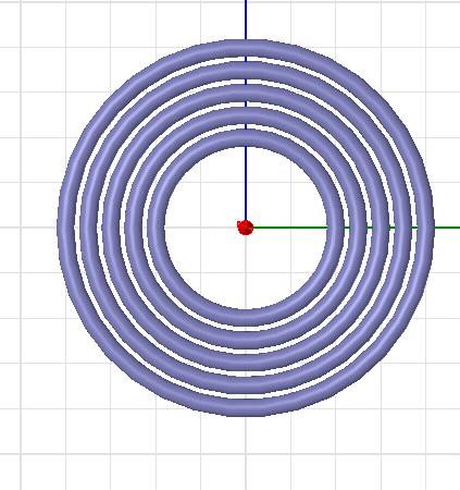
16 Hierarchical Modeling of Coils Consisting of Litz Wires 30A Page 16

17 Potential Distribution in Copper-Ceramics Substrate Copper at 10 kv Gel Conducting interlayer Ceramic Layer 1 Ceramic Layer 2 Copper at 0kV Page 17


18 Coupling of Process Simulation and Electrical Characterization Simulated interconnect geometry Current density distribution simulated with STAP, TU Vienna Page 18
Plasma Deposition (Overview) Lecture 1
 Lecture 1") Plasma Deposition (Overview) Lecture 1 Material Processes Plasma Processing Plasma-assisted Deposition Implantation Surface Modification Development of Plasma-based processing Microelectronics needs (fabrication
Plasma Deposition (Overview) Lecture 1 Material Processes Plasma Processing Plasma-assisted Deposition Implantation Surface Modification Development of Plasma-based processing Microelectronics needs (fabrication
ETCHING Chapter 10. Mask. Photoresist
 ETCHING Chapter 10 Mask Light Deposited Substrate Photoresist Etch mask deposition Photoresist application Exposure Development Etching Resist removal Etching of thin films and sometimes the silicon substrate
Film Deposition Part 1
 1 Film Deposition Part 1 Chapter 11 : Semiconductor Manufacturing Technology by M. Quirk & J. Serda Spring Semester 2013 Saroj Kumar Patra Semidonductor Manufacturing Technology, Norwegian University of
EE143 Fall 2016 Microfabrication Technologies. Lecture 6: Thin Film Deposition Reading: Jaeger Chapter 6
 EE143 Fall 2016 Microfabrication Technologies Lecture 6: Thin Film Deposition Reading: Jaeger Chapter 6 Prof. Ming C. Wu wu@eecs.berkeley.edu 511 Sutardja Dai Hall (SDH) 1 Vacuum Basics Units 1 atmosphere
Fabrication Technology, Part I
 EEL5225: Principles of MEMS Transducers (Fall 2004) Fabrication Technology, Part I Agenda: Microfabrication Overview Basic semiconductor devices Materials Key processes Oxidation Thin-film Deposition Reading:
Taurus-Topography. Topography Modeling for IC Technology
 SYSTEMS PRODUCTS LOGICAL PRODUCTS PHYSICAL IMPLEMENTATION SIMULATION AND ANALYSIS LIBRARIES TCAD Aurora DFM WorkBench Davinci Medici Raphael Raphael-NES Silicon Early Access TSUPREM-4 Taurus-Device Taurus-Lithography
SCALING OF HOLLOW CATHODE MAGNETRONS FOR METAL DEPOSITION a)
") SCALING OF HOLLOW CATHODE MAGNETRONS FOR METAL DEPOSITION a) Gabriel Font b) Novellus Systems, Inc. San Jose, CA, 95134 USA and Mark J. Kushner Dept. of Electrical and Computer Engineering Urbana, IL,
SCALING OF HOLLOW CATHODE MAGNETRONS FOR METAL DEPOSITION a) Gabriel Font b) Novellus Systems, Inc. San Jose, CA, 95134 USA and Mark J. Kushner Dept. of Electrical and Computer Engineering Urbana, IL,
4FNJDPOEVDUPS 'BCSJDBUJPO &UDI
 2010.5.4 1 Major Fabrication Steps in CMOS Process Flow UV light oxygen Silicon dioxide Silicon substrate Oxidation (Field oxide) photoresist Photoresist Coating Mask exposed photoresist Mask-Wafer Exposed
Section 5: Thin Film Deposition part 1 : sputtering and evaporation. Jaeger Chapter 6. EE143 Ali Javey
 Section 5: Thin Film Deposition part 1 : sputtering and evaporation Jaeger Chapter 6 Vacuum Basics 1. Units 1 atmosphere = 760 torr = 1.013x10 5 Pa 1 bar = 10 5 Pa = 750 torr 1 torr = 1 mm Hg 1 mtorr =
MODELING OF SEASONING OF REACTORS: EFFECTS OF ION ENERGY DISTRIBUTIONS TO CHAMBER WALLS*
 MODELING OF SEASONING OF REACTORS: EFFECTS OF ION ENERGY DISTRIBUTIONS TO CHAMBER WALLS* Ankur Agarwal a) and Mark J. Kushner b) a) Department of Chemical and Biomolecular Engineering University of Illinois,
CVD: General considerations.
 CVD: General considerations. PVD: Move material from bulk to thin film form. Limited primarily to metals or simple materials. Limited by thermal stability/vapor pressure considerations. Typically requires
DEPOSITION AND COMPOSITION OF POLYMER FILMS IN FLUOROCARBON PLASMAS*
 DEPOSITION AND COMPOSITION OF POLYMER FILMS IN FLUOROCARBON PLASMAS* Kapil Rajaraman and Mark J. Kushner 1406 W. Green St. Urbana, IL 61801 rajaramn@uiuc.edu mjk@uiuc.edu http://uigelz.ece.uiuc.edu November
UHF-ECR Plasma Etching System for Dielectric Films of Next-generation Semiconductor Devices
 UHF-ECR Plasma Etching System for Dielectric Films of Next-generation Semiconductor Devices 1 UHF-ECR Plasma Etching System for Dielectric Films of Next-generation Semiconductor Devices Katsuya Watanabe
Plasma Chemistry Study in an Inductively Coupled Dielectric Etcher
 Plasma Chemistry Study in an Inductively Coupled Dielectric Etcher Chunshi Cui, John Trow, Ken Collins, Betty Tang, Luke Zhang, Steve Shannon, and Yan Ye Applied Materials, Inc. October 26, 2000 10/28/2008
Lecture 6 Plasmas. Chapters 10 &16 Wolf and Tauber. ECE611 / CHE611 Electronic Materials Processing Fall John Labram 1/68
 Lecture 6 Plasmas Chapters 10 &16 Wolf and Tauber 1/68 Announcements Homework: Homework will be returned to you on Thursday (12 th October). Solutions will be also posted online on Thursday (12 th October)
Repetition: Practical Aspects
 Repetition: Practical Aspects Reduction of the Cathode Dark Space! E x 0 Geometric limit of the extension of a sputter plant. Lowest distance between target and substrate V Cathode (Target/Source) - +
INTRODUCTION TO THE HYBRID PLASMA EQUIPMENT MODEL
 INTRODUCTION TO THE HYBRID PLASMA EQUIPMENT MODEL Prof. Mark J. Kushner Department of Electrical and Computer Engineering 1406 W. Green St. Urbana, IL 61801 217-144-5137 mjk@uiuc.edu http://uigelz.ece.uiuc.edu
LECTURE 5 SUMMARY OF KEY IDEAS
 LECTURE 5 SUMMARY OF KEY IDEAS Etching is a processing step following lithography: it transfers a circuit image from the photoresist to materials form which devices are made or to hard masking or sacrificial
3.155J/6.152J Microelectronic Processing Technology Fall Term, 2004
 3.155J/6.152J Microelectronic Processing Technology Fall Term, 2004 Bob O'Handley Martin Schmidt Quiz Nov. 17, 2004 Ion implantation, diffusion [15] 1. a) Two identical p-type Si wafers (N a = 10 17 cm
Thin Film Deposition. Reading Assignments: Plummer, Chap 9.1~9.4
 Thin Film Deposition Reading Assignments: Plummer, Chap 9.1~9.4 Thermally grown Deposition Thin Film Formation Thermally grown SiO 2 Deposition SiO 2 Oxygen is from gas phase Silicon from substrate Oxide
SPUTTER-WIND HEATING IN IONIZED METAL PVD+
 SPUTTER-WIND HEATING IN IONIZED METAL PVD+ Junqing Lu* and Mark Kushner** *Department of Mechanical and Industrial Engineering **Department of Electrical and Computer Engineering University of Illinois
SIMULATION OF POROUS LOW-k DIELECTRIC SEALING BY COMBINED He AND NH 3 PLASMA TREATMENT *
 SIMULATION OF POROUS LOW-k DIELECTRIC SEALING BY COMBINED He AND NH 3 PLASMA TREATMENT * JULINE_ICOPS09_01 Juline Shoeb a) and Mark J. Kushner b) a) Department of Electrical and Computer Engineering Iowa
Chapter 7. Plasma Basics
 Chapter 7 Plasma Basics 2006/4/12 1 Objectives List at least three IC processes using plasma Name three important collisions in plasma Describe mean free path Explain how plasma enhance etch and CVD processes
In situ electrical characterization of dielectric thin films directly exposed to plasma vacuum-ultraviolet radiation
 JOURNAL OF APPLIED PHYSICS VOLUME 88, NUMBER 4 15 AUGUST 2000 In situ electrical characterization of dielectric thin films directly exposed to plasma vacuum-ultraviolet radiation C. Cismaru a) and J. L.
Chapter 7 Plasma Basic
 Chapter 7 Plasma Basic Hong Xiao, Ph. D. hxiao89@hotmail.com www2.austin.cc.tx.us/hongxiao/book.htm Hong Xiao, Ph. D. www2.austin.cc.tx.us/hongxiao/book.htm 1 Objectives List at least three IC processes
Device Fabrication: Etch
 Device Fabrication: Etch 1 Objectives Upon finishing this course, you should able to: Familiar with etch terminology Compare wet and dry etch processes processing and list the main dry etch etchants Become
Technology for Micro- and Nanostructures Micro- and Nanotechnology
 Lecture 10: Deposition Technology for Micro- and Nanostructures Micro- and Nanotechnology Peter Unger mailto: peter.unger @ uni-ulm.de Institute of Optoelectronics University of Ulm http://www.uni-ulm.de/opto
Alternative deposition solution for cost reduction of TSV integration
 Alternative deposition solution for cost reduction of TSV integration J. Vitiello, F. Piallat, L. Bonnet KOBUS 611 rue Aristide Bergès, Z.A. de Pré Millet, Montbonnot-Saint-Martin, 38330 France Ph: +33
Reactive Ion Etching (RIE)
") Reactive Ion Etching (RIE) RF 13.56 ~ MHz plasma Parallel-Plate Reactor wafers Sputtering Plasma generates (1) Ions (2) Activated neutrals Enhance chemical reaction 1 2 Remote Plasma Reactors Plasma Sources
Reactive Ion Etching (RIE) RF 13.56 ~ MHz plasma Parallel-Plate Reactor wafers Sputtering Plasma generates (1) Ions (2) Activated neutrals Enhance chemical reaction 1 2 Remote Plasma Reactors Plasma Sources
6.5 Optical-Coating-Deposition Technologies
 92 Chapter 6 6.5 Optical-Coating-Deposition Technologies The coating process takes place in an evaporation chamber with a fully controlled system for the specified requirements. Typical systems are depicted
Gaetano L Episcopo. Scanning Electron Microscopy Focus Ion Beam and. Pulsed Plasma Deposition
 Gaetano L Episcopo Scanning Electron Microscopy Focus Ion Beam and Pulsed Plasma Deposition Hystorical background Scientific discoveries 1897: J. Thomson discovers the electron. 1924: L. de Broglie propose
MICROCHIP MANUFACTURING by S. Wolf
 by S. Wolf Chapter 15 ALUMINUM THIN-FILMS and SPUTTER-DEPOSITION 2004 by LATTICE PRESS CHAPTER 15 - CONTENTS Aluminum Thin-Films Sputter-Deposition Process Steps Physics of Sputter-Deposition Magnetron-Sputtering
TMT4320 Nanomaterials November 10 th, Thin films by physical/chemical methods (From chapter 24 and 25)
") 1 TMT4320 Nanomaterials November 10 th, 2015 Thin films by physical/chemical methods (From chapter 24 and 25) 2 Thin films by physical/chemical methods Vapor-phase growth (compared to liquid-phase growth)
1 TMT4320 Nanomaterials November 10 th, 2015 Thin films by physical/chemical methods (From chapter 24 and 25) 2 Thin films by physical/chemical methods Vapor-phase growth (compared to liquid-phase growth)
Etching: Basic Terminology
 Lecture 7 Etching Etching: Basic Terminology Introduction : Etching of thin films and sometimes the silicon substrate are very common process steps. Usually selectivity, and directionality are the first
Transistor and Integrated Circuits: History
 Course Objective Review and practice fundamental chemical engineering concepts (mass, energy, and momentum transport coupled with heterogeneous and homogeneous reactions and thermodynamics). Apply these
Etching Issues - Anisotropy. Dry Etching. Dry Etching Overview. Etching Issues - Selectivity
 Etching Issues - Anisotropy Dry Etching Dr. Bruce K. Gale Fundamentals of Micromachining BIOEN 6421 EL EN 5221 and 6221 ME EN 5960 and 6960 Isotropic etchants etch at the same rate in every direction mask
Section 3: Etching. Jaeger Chapter 2 Reader
 Section 3: Etching Jaeger Chapter 2 Reader Etch rate Etch Process - Figures of Merit Etch rate uniformity Selectivity Anisotropy d m Bias and anisotropy etching mask h f substrate d f d m substrate d f
Nova 600 NanoLab Dual beam Focused Ion Beam IITKanpur
 Nova 600 NanoLab Dual beam Focused Ion Beam system @ IITKanpur Dual Beam Nova 600 Nano Lab From FEI company (Dual Beam = SEM + FIB) SEM: The Electron Beam for SEM Field Emission Electron Gun Energy : 500
ALD & ALE Tutorial Speakers and Schedule
 ALD & ALE Tutorial Speakers and Schedule Sunday, July 29, 2018 1:00-1:05 Tutorial Welcome 1:05-1:50 1:50-2:35 2:35-3:20 Challenges of ALD Applications in Memory Semiconductor Devices, Choon Hwan Kim (SK
Self-study problems and questions Processing and Device Technology, FFF110/FYSD13
 Self-study problems and questions Processing and Device Technology, FFF110/FYSD13 Version 2016_01 In addition to the problems discussed at the seminars and at the lectures, you can use this set of problems
Plasma-Surface Interactions in Patterning High-k k Dielectric Materials
 Plasma-Surface Interactions in Patterning High-k k Dielectric Materials October 11, 4 Feature Level Compensation and Control Seminar Jane P. Chang Department of Chemical Engineering University of California,
Feature Profile Evolution during Shallow Trench Isolation (STI) Etch in Chlorine-based Plasmas
 Etch in Chlorine-based Plasmas") 1 Feature Profile Evolution during Shallow Trench Isolation (STI) Etch in Chlorine-based Plasmas Presentation November 14, 2005 Jane P. Chang and John Hoang Department of Chemical and Biomolecular Engineering
1 Feature Profile Evolution during Shallow Trench Isolation (STI) Etch in Chlorine-based Plasmas Presentation November 14, 2005 Jane P. Chang and John Hoang Department of Chemical and Biomolecular Engineering
Case Study of Electronic Materials Packaging with Poor Metal Adhesion and the Process for Performing Root Cause Failure Analysis
 Case Study of Electronic Materials Packaging with Poor Metal Adhesion and the Process for Performing Root Cause Failure Analysis Dr. E. A. Leone BACKGRUND ne trend in the electronic packaging industry
EE 527 MICROFABRICATION. Lecture 25 Tai-Chang Chen University of Washington
 EE 527 MICROFABRICATION Lecture 25 Tai-Chang Chen University of Washington ION MILLING SYSTEM Kaufmann source Use e-beam to strike plasma A magnetic field applied to increase ion density Drawback Low etch
Introduction to Plasma
 What is a plasma? The fourth state of matter A partially ionized gas How is a plasma created? Energy must be added to a gas in the form of: Heat: Temperatures must be in excess of 4000 O C Radiation Electric
Sensors and Metrology. Outline
 Sensors and Metrology A Survey 1 Outline General Issues & the SIA Roadmap Post-Process Sensing (SEM/AFM, placement) In-Process (or potential in-process) Sensors temperature (pyrometry, thermocouples, acoustic
Application of Rarefied Flow & Plasma Simulation Software
 2016/5/18 Application of Rarefied Flow & Plasma Simulation Software Yokohama City in Japan Profile of Wave Front Co., Ltd. Name : Wave Front Co., Ltd. Incorporation : March 1990 Head Office : Yokohama
Carbon Nanotubes for Interconnect Applications Franz Kreupl, Andrew P. Graham, Maik Liebau, Georg S. Duesberg, Robert Seidel, Eugen Unger
 Carbon Nanotubes for Interconnect Applications Franz Kreupl, Andrew P. Graham, Maik Liebau, Georg S. Duesberg, Robert Seidel, Eugen Unger Infineon Technologies Corporate Research Munich, Germany Outline
E SC 412 Nanotechnology: Materials, Infrastructure, and Safety Wook Jun Nam
 E SC 412 Nanotechnology: Materials, Infrastructure, and Safety Wook Jun Nam Lecture 10 Outline 1. Wet Etching/Vapor Phase Etching 2. Dry Etching DC/RF Plasma Plasma Reactors Materials/Gases Etching Parameters
PIC-MCC/Fluid Hybrid Model for Low Pressure Capacitively Coupled O 2 Plasma
 PIC-MCC/Fluid Hybrid Model for Low Pressure Capacitively Coupled O 2 Plasma Kallol Bera a, Shahid Rauf a and Ken Collins a a Applied Materials, Inc. 974 E. Arques Ave., M/S 81517, Sunnyvale, CA 9485, USA
Supplementary Information
 Supplementary Information Supplementary Figure 1. fabrication. A schematic of the experimental setup used for graphene Supplementary Figure 2. Emission spectrum of the plasma: Negative peaks indicate an
Sputtering by Particle Bombardment
 Rainer Behrisch, Wolfgang Eckstein (Eds.) Sputtering by Particle Bombardment Experiments and Computer Calculations from Threshold to MeV Energies With 201 Figures e1 Springer Contents Introduction and
UNIVERSITY OF CALIFORNIA College of Engineering Department of Electrical Engineering and Computer Sciences. Fall Exam 1
 UNIVERSITY OF CALIFORNIA College of Engineering Department of Electrical Engineering and Computer Sciences EECS 143 Fall 2008 Exam 1 Professor Ali Javey Answer Key Name: SID: 1337 Closed book. One sheet
Wet and Dry Etching. Theory
 Wet and Dry Etching Theory 1. Introduction Etching techniques are commonly used in the fabrication processes of semiconductor devices to remove selected layers for the purposes of pattern transfer, wafer
SUPPLEMENTARY NOTES Supplementary Note 1: Fabrication of Scanning Thermal Microscopy Probes
 SUPPLEMENTARY NOTES Supplementary Note 1: Fabrication of Scanning Thermal Microscopy Probes Fabrication of the scanning thermal microscopy (SThM) probes is summarized in Supplementary Fig. 1 and proceeds
Plasma Technology September 15, 2005 A UC Discovery Project
 1 Feature-level Compensation & Control Plasma Technology September 15, 2005 A UC Discovery Project 9/15/05 - Plasma Technology 2 Plasma Technology Professors Jane P. Chang (UCLA), Michael A. Lieberman,
OPTIMIZATION OF DIELECTRICS SURFACE PREPARATION FOR VACUUM COATING
 OPTIMIZATION OF DIELECTRICS SURFACE PREPARATION FOR VACUUM COATING Dr. Boris Statnikov Introduction Modern MICRO and NANO technologies in ultra- and high-frequency electronics are widely focused on application
Vapor-Phase Cutting of Carbon Nanotubes Using a Nanomanipulator Platform
 Vapor-Phase Cutting of Carbon Nanotubes Using a Nanomanipulator Platform MS&T 10, October 18, 2010 Vladimir Mancevski, President and CTO, Xidex Corporation Philip D. Rack, Professor, The University of
Simulation of Ion Beam Etching of Patterned Nanometer-scale Magnetic Structures for High-Density Storage Applications
 Engineered Excellence A Journal for Process and Device Engineers Simulation of Ion Beam Etching of Patterned Nanometer-scale Magnetic Structures for High-Density Storage Applications Introduction Fabrication
Imaging Methods: Scanning Force Microscopy (SFM / AFM)
") Imaging Methods: Scanning Force Microscopy (SFM / AFM) The atomic force microscope (AFM) probes the surface of a sample with a sharp tip, a couple of microns long and often less than 100 Å in diameter.
Imaging Methods: Scanning Force Microscopy (SFM / AFM) The atomic force microscope (AFM) probes the surface of a sample with a sharp tip, a couple of microns long and often less than 100 Å in diameter.
Auger Electron Spectroscopy
 Auger Electron Spectroscopy Auger Electron Spectroscopy is an analytical technique that provides compositional information on the top few monolayers of material. Detect all elements above He Detection
Feature-level Compensation & Control
 Feature-level Compensation & Control 2 Plasma Eray Aydil, UCSB, Mike Lieberman, UCB and David Graves UCB Workshop November 19, 2003 Berkeley, CA 3 Feature Profile Evolution Simulation Eray S. Aydil University
Chapter 3 Engineering Science for Microsystems Design and Fabrication
 Lectures on MEMS and MICROSYSTEMS DESIGN and MANUFACTURE Chapter 3 Engineering Science for Microsystems Design and Fabrication In this Chapter, we will present overviews of the principles of physical and
Trench filling by ionized metal physical vapor deposition
 Trench filling by ionized metal physical vapor deposition Junqing Lu a) and Mark J. Kushner b) University of Illinois, 1406 W. Green Street, Urbana, Illinois 61801 Received 25 January 2001; accepted 16
Dry Etching Zheng Yang ERF 3017, MW 5:15-6:00 pm
 Dry Etching Zheng Yang ERF 3017, email: yangzhen@uic.edu, MW 5:15-6:00 pm Page 1 Page 2 Dry Etching Why dry etching? - WE is limited to pattern sizes above 3mm - WE is isotropic causing underetching -
Chapter 6. Summary and Conclusions
 Chapter 6 Summary and Conclusions Plasma deposited amorphous hydrogenated carbon films (a-c:h) still attract a lot of interest due to their extraordinary properties. Depending on the deposition conditions
The plasma simulation system Brochure.
 1 The plasma simulation system 2016 Brochure www.quantemol.com 2 What does Q-VT do? Quantemol-Virtual Tool is an expert software system for the simulation of industrial plasma processing tools. Q-VT builds
Enhanced High Aspect Ratio Etch Performance With ANAB Technology. Keywords: High Aspect Ratio, Etch, Neutral Particles, Neutral Beam I.
 Enhanced High Aspect Ratio Etch Performance With ANAB Technology. Keywords: High Aspect Ratio, Etch, Neutral Particles, Neutral Beam I. INTRODUCTION As device density increases according to Moore s law,
PIC-MCC/Fluid Hybrid Model for Low Pressure Capacitively Coupled O 2 Plasma
 PIC-MCC/Fluid Hybrid Model for Low Pressure Capacitively Coupled O 2 Plasma Kallol Bera a, Shahid Rauf a and Ken Collins a a Applied Materials, Inc. 974 E. Arques Ave., M/S 81517, Sunnyvale, CA 9485, USA
Repetition: Ion Plating
 Repetition: Ion Plating Substrate HV (bis ca. 1kV) Optional ionization system Source Ionized filling gas Source material, ionized or neutral Repetition: Ion Plating Ion Species Separated ion source Ions
Direct-Write Deposition Utilizing a Focused Electron Beam
 Direct-Write Deposition Utilizing a Focused Electron Beam M. Fischer, J. Gottsbachner, S. Müller, W. Brezna, and H.D. Wanzenboeck Institute of Solid State Electronics, Vienna University of Technology,
Solutions for Assignment-6
 Solutions for Assignment-6 Q1. What is the aim of thin film deposition? [1] (a) To maintain surface uniformity (b) To reduce the amount (or mass) of light absorbing materials (c) To decrease the weight
X- ray Photoelectron Spectroscopy and its application in phase- switching device study
 X- ray Photoelectron Spectroscopy and its application in phase- switching device study Xinyuan Wang A53073806 I. Background X- ray photoelectron spectroscopy is of great importance in modern chemical and
INVESTIGATION of Si and SiO 2 ETCH MECHANISMS USING an INTEGRATED SURFACE KINETICS MODEL
 46 th AVS International Symposium Oct. 25-29, 1999 Seattle, WA INVESTIGATION of Si and SiO 2 ETCH MECHANISMS USING an INTEGRATED SURFACE KINETICS MODEL Da Zhang* and Mark J. Kushner** *Department of Materials
MODELING OF AN ECR SOURCE FOR MATERIALS PROCESSING USING A TWO DIMENSIONAL HYBRID PLASMA EQUIPMENT MODEL. Ron L. Kinder and Mark J.
 TECHCON 98 Las Vegas, Nevada September 9-11, 1998 MODELING OF AN ECR SOURCE FOR MATERIALS PROCESSING USING A TWO DIMENSIONAL HYBRID PLASMA EQUIPMENT MODEL Ron L. Kinder and Mark J. Kushner Department of
Plasma Etching: Atomic Scale Surface Fidelity and 2D Materials
 1 Plasma Etching: Atomic Scale Surface Fidelity and 2D Materials Thorsten Lill, Keren J. Kanarik, Samantha Tan, Meihua Shen, Alex Yoon, Eric Hudson, Yang Pan, Jeffrey Marks, Vahid Vahedi, Richard A. Gottscho
SIMULATIONS OF ECR PROCESSING SYSTEMS SUSTAINED BY AZIMUTHAL MICROWAVE TE(0,n) MODES*
 MODES*") 25th IEEE International Conference on Plasma Science Raleigh, North Carolina June 1-4, 1998 SIMULATIONS OF ECR PROCESSING SYSTEMS SUSTAINED BY AZIMUTHAL MICROWAVE TE(,n) MODES* Ron L. Kinder and Mark J.
25th IEEE International Conference on Plasma Science Raleigh, North Carolina June 1-4, 1998 SIMULATIONS OF ECR PROCESSING SYSTEMS SUSTAINED BY AZIMUTHAL MICROWAVE TE(,n) MODES* Ron L. Kinder and Mark J.
Focused Ion Beam Induced Local Tungsten Deposition
 Focused Ion Beam Induced Local Tungsten Deposition H. Langfischer, B. Basnar, E. Bertagnolli Institute for Solid State Electronics, Vienna University of Technology, Floragasse 7, 1040 ien, Austria H. Hutter
Supplementary Figure 1 Detailed illustration on the fabrication process of templatestripped
 Supplementary Figure 1 Detailed illustration on the fabrication process of templatestripped gold substrate. (a) Spin coating of hydrogen silsesquioxane (HSQ) resist onto the silicon substrate with a thickness
EE 527 MICROFABRICATION. Lecture 24 Tai-Chang Chen University of Washington
 EE 527 MICROFABRICATION Lecture 24 Tai-Chang Chen University of Washington EDP ETCHING OF SILICON - 1 Ethylene Diamine Pyrocatechol Anisotropy: (100):(111) ~ 35:1 EDP is very corrosive, very carcinogenic,
arxiv: v1 [physics.plasm-ph] 10 Nov 2014
![arxiv: v1 [physics.plasm-ph] 10 Nov 2014](/thumbs/88/117240344.jpg "arxiv: v1 [physics.plasm-ph] 10 Nov 2014") arxiv:1411.2464v1 [physics.plasm-ph] 10 Nov 2014 Effects of fast atoms and energy-dependent secondary electron emission yields in PIC/MCC simulations of capacitively coupled plasmas A. Derzsi 1, I. Korolov
arxiv:1411.2464v1 [physics.plasm-ph] 10 Nov 2014 Effects of fast atoms and energy-dependent secondary electron emission yields in PIC/MCC simulations of capacitively coupled plasmas A. Derzsi 1, I. Korolov
Supplementary Information Our InGaN/GaN multiple quantum wells (MQWs) based one-dimensional (1D) grating structures
 based one-dimensional (1D) grating structures") Polarized white light from hybrid organic/iii-nitrides grating structures M. Athanasiou, R. M. Smith, S. Ghataora and T. Wang* Department of Electronic and Electrical Engineering, University of Sheffield,
Polarized white light from hybrid organic/iii-nitrides grating structures M. Athanasiou, R. M. Smith, S. Ghataora and T. Wang* Department of Electronic and Electrical Engineering, University of Sheffield,
Effects of plasma treatment on the precipitation of fluorine-doped silicon oxide
 ARTICLE IN PRESS Journal of Physics and Chemistry of Solids 69 (2008) 555 560 www.elsevier.com/locate/jpcs Effects of plasma treatment on the precipitation of fluorine-doped silicon oxide Jun Wu a,, Ying-Lang
Procédés de dépôt plasma avec injection pulsée de précurseurs (PECVD et PEALD) :
 :") Procédés de dépôt plasma avec injection pulsée de précurseurs (PECVD et PEALD) : Impact du réacteur et de la pression et développement de dépôts sélectifs C. Vallée 1,3, R. Gassilloud 2, R. Vallat 1,2,
Procédés de dépôt plasma avec injection pulsée de précurseurs (PECVD et PEALD) : Impact du réacteur et de la pression et développement de dépôts sélectifs C. Vallée 1,3, R. Gassilloud 2, R. Vallat 1,2,
Outlines 3/12/2011. Vacuum Chamber. Inside the sample chamber. Nano-manipulator. Focused ion beam instrument. 1. Other components of FIB instrument
 Focused ion beam instruments Outlines 1. Other components of FIB instrument 1.a Vacuum chamber 1.b Nanomanipulator 1.c Gas supply for deposition 1.d Detectors 2. Capabilities of FIB instrument Lee Chow
Effect of Gas Flow Rate and Gas Composition in Ar/CH 4 Inductively Coupled Plasmas
 COMSOL CONFERENCE BOSTON 2011 Effect of Gas Flow Rate and Gas Composition in Ar/CH 4 Inductively Coupled Plasmas Keisoku Engineering System Co., Ltd., JAPAN Dr. Lizhu Tong October 14, 2011 1 Contents 1.
Table of Content. Mechanical Removing Techniques. Ultrasonic Machining (USM) Sputtering and Focused Ion Beam Milling (FIB)
 Sputtering and Focused Ion Beam Milling (FIB)") Table of Content Mechanical Removing Techniques Ultrasonic Machining (USM) Sputtering and Focused Ion Beam Milling (FIB) Ultrasonic Machining In ultrasonic machining (USM), also called ultrasonic grinding,
Table of Content Mechanical Removing Techniques Ultrasonic Machining (USM) Sputtering and Focused Ion Beam Milling (FIB) Ultrasonic Machining In ultrasonic machining (USM), also called ultrasonic grinding,
Semiconductor Technology
 Semiconductor Technology from A to Z Deposition www.halbleiter.org Contents Contents List of Figures II 1 Deposition 1 1.1 Plasma, the fourth aggregation state of a material............. 1 1.1.1 Plasma
Photoresist Profile. Undercut: negative slope, common for negative resist; oxygen diffusion prohibits cross-linking; good for lift-off.
 Photoresist Profile 4-15 Undercut: negative slope, common for negative resist; oxygen diffusion prohibits cross-linking; good for lift-off undercut overcut Overcut: positive slope, common to positive resist,
EE C245 ME C218 Introduction to MEMS Design Fall 2007
 EE C245 ME C218 Introduction to MEMS Design Fall 2007 Prof. Clark T.-C. Nguyen Dept. of Electrical Engineering & Computer Sciences University of California at Berkeley Berkeley, CA 94720 Lecture 4: Film
Auger Electron Spectroscopy (AES)
") 1. Introduction Auger Electron Spectroscopy (AES) Silvia Natividad, Gabriel Gonzalez and Arena Holguin Auger Electron Spectroscopy (Auger spectroscopy or AES) was developed in the late 1960's, deriving
1. Introduction Auger Electron Spectroscopy (AES) Silvia Natividad, Gabriel Gonzalez and Arena Holguin Auger Electron Spectroscopy (Auger spectroscopy or AES) was developed in the late 1960's, deriving
Scaling up Chemical Vapor Deposition Graphene to 300 mm Si substrates
 Scaling up Chemical Vapor Deposition Graphene to 300 mm Si substrates Co- Authors Aixtron Alex Jouvray Simon Buttress Gavin Dodge Ken Teo The work shown here has received partial funding from the European
EE 292L : Nanomanufacturing. Week 5: Advanced Process Technology. Oct
 EE 292L : Nanomanufacturing Week 5: Advanced Process Technology Oct 22 2012 1 Advanced Process Technology 1 HAR etch 2 3 HAR Gapfill Metal ALD 4 Reflow 5 6 SAC Airgap 7 8 Strain Ge/III-V Engineering 1
Manufacturable AlGaAs/GaAs HBT Implant Isolation Process Using Doubly Charged Helium
 Manufacturable AlGaAs/GaAs HBT Implant Isolation Process Using Doubly Charged Helium ABSTRACT Rainier Lee, Shiban Tiku, and Wanming Sun Conexant Systems 2427 W. Hillcrest Drive Newbury Park, CA 91320 (805)
SURFACE ENGINEERING MASS SPECTROMETERS FOR THIN FILMS, PLASMA AND SURFACE ENGINEERING
 SURFACE ENGINEERING MASS SPECTROMETERS FOR THIN FILMS, PLASMA AND SURFACE ENGINEERING HIDEN MS MASS SPECTROMETERS for Thin Films and Surface Engineering Hiden Analytical have been designing and developing
Metal Deposition. Filament Evaporation E-beam Evaporation Sputter Deposition
 Metal Deposition Filament Evaporation E-beam Evaporation Sputter Deposition 1 Filament evaporation metals are raised to their melting point by resistive heating under vacuum metal pellets are placed on
Fabrication and Characterization of Silicon Rich Oxide (SRO) Thin Film Deposited by Plasma Enhanced CVD for Si Quantum Dot
 Thin Film Deposited by Plasma Enhanced CVD for Si Quantum Dot") Fabrication and Characterization of Silicon Rich Oxide (SRO) Thin Film Deposited by Plasma Enhanced CVD for Si Quantum Dot By Tian Zhang School of Photovoltaic and Renewable Energy Engineering Technology
Fabrication and Characterization of Silicon Rich Oxide (SRO) Thin Film Deposited by Plasma Enhanced CVD for Si Quantum Dot By Tian Zhang School of Photovoltaic and Renewable Energy Engineering Technology
Plasma atomic layer etching using conventional plasma equipment
 Plasma atomic layer etching using conventional plasma equipment Ankur Agarwal a Department of Chemical and Biomolecular Engineering, University of Illinois, 600 S. Mathews Ave., Urbana, Illinois 61801
EE143 LAB. Professor N Cheung, U.C. Berkeley
 EE143 LAB 1 1 EE143 Equipment in Cory 218 2 Guidelines for Process Integration * A sequence of Additive and Subtractive steps with lateral patterning Processing Steps Si wafer Watch out for materials compatibility
A Mechanical Model for Erosion in Copper Chemical-Mechanical Polishing
 A Mechanical Model for Erosion in Copper Chemical-Mechanical Polishing Kyungyoon Noh, Nannaji Saka and Jung-Hoon Chun Laboratory for Manufacturing and Productivity Massachusetts Institute of Technology