Table of Content. Mechanical Removing Techniques. Ultrasonic Machining (USM) Sputtering and Focused Ion Beam Milling (FIB)
|
|
|
- Eunice Patrick
- 5 years ago
- Views:
Transcription
1 Table of Content Mechanical Removing Techniques Ultrasonic Machining (USM) Sputtering and Focused Ion Beam Milling (FIB)


2 Ultrasonic Machining In ultrasonic machining (USM), also called ultrasonic grinding, highfrequency vibrations delivered to a tool tip, embedded in an abrasive slurry, by a booster or sonotrode, create accurate cavities of virtually any shape; that are, negatives of the tool. Since this method is non-thermal, non-electrical, and non-chemical, it produces virtually stress-free shapes even in hard and brittle work-pieces. Ultrasonic drilling is most effective for hard and brittle materials; soft materials absorb too much sound energy and make the process less efficient.
, and is often made from a softer material than the workpiece, say from brass, cold-rolled steel, or stainless steel")
3 Almost any hard and brittle material, including aluminum oxides, silicon, silicon carbide, silicon nitride, glass, quartz, sapphire, ferrite, fiber optics, etc., can be ultrasonically machined. The tool does not exert any pressure on the work-piece (drilling without drills), and is often made from a softer material than the workpiece, say from brass, cold-rolled steel, or stainless steel and wears only slightly. The roots of ultrasonic technology can be traced back to research on the piezoelectric effect conducted by Pierre Curie around He found that asymmetrical crystals such as quartz and Rochelle salt (potassium sodium titrate) generate an electric charge when mechanical pressure is applied. Conversely, mechanical vibrations are obtained by applying electrical oscillations to the same crystals. Ultrasonic waves are sound waves of frequency higher than 20,000 Hz. Ultrasonic Machining

4 The tool, typically vibrating at a low amplitude of mm at a frequency of 20 to 100 khz, is gradually fed into the work-piece to form a cavity corresponding to the tool shape. The vibration transmits a high velocity force to fine abrasive grains between the tool and the surface of the workpiece. In the process material is removed by micro-chipping or erosion with the abrasive particles. The grains are in a water slurry which also serves to remove debris from the cutting area. The high-frequency power supply for the magnetostrictive or piezoelectric transducer stack that drives the tool is typically rated between 0.1 and 40 kw. Ultrasonic Machining Channels and holes ultrasonically machined in a polycrystalline silicon wafer.

5 Ultrasonic Machining Coin with grooving carried out with USM The abrasive particles (SiC, Al 2 O 3 or BC d= 8~ 500 µm) are suspended in water or oil. The particle size and the vibration amplitude are ususally made about the same. The particle size determines the roughness or surface finish and the speed of the cut. Material removal rates are quite low, usually less than 50 mm 3 /min.
 to the modulus of elasticity (E).")
6 Ultrasonic Machining The mechanical properties and fracture behavior of the work-piece materials also play a large role in both roughness and cutting speed. For a given grit size of the abrasive, the resulting surface roughness depends on the ratio of the hardness (H) to the modulus of elasticity (E). As this ratio increases, the surface roughness increases. Higher H/E ratios also lead to higher removal rates: 4 mm 3 /min for carbide and 11 mm 3 /min for glass. ultrasonic machining can be used to form intricate, finely detailed graphite electrodes.

7 Ultrasonic Machining Machines cost up to $20,000, and production rates of about 2500 parts per machine per day are typical. If the machined part is a complex element (e.g., a fluidic element) of a size > 1 cm 2 and the best material to be used is an inert, hard ceramic, this machining method might well be the most appropriate 900 watt Sonic-mill, Ultrasonic Mill
8 Ultrasonic Machining Advantages and disadvantages of ultrasonic machining. Advantages Machining of any material regardless of conductivity Precision machining of brittle hard materials Does not produce electric, thermal or chemical defe cts at the surfa ce Can drill circular or non-circular holes in very hard materials Less stress because of its non-thermal nature Disadvantages Low material removal rate Tool wears fast Machining area and depth are quite restricted
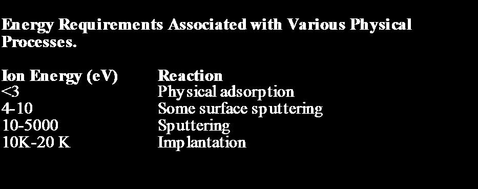
9 Sputtering Talking about sputtering we usually mean the usage of the phenomena which are going on at the surface of solids (target) exposed in vacuum under the directed flow of atomic particles - ions or neutrals. Ions are extracted from gas discharge plasma as a spatially restricted beam and accelerated by the electric field to the required energies. Usually for the purposes of sputtering we use the energy band from about 100 ev to 5000 ev (for ion implantation, energies up to a few tens kev may be used) (see figure on next slide). What happens when ions with energy 0,1-5 kev bombard the surface of the solid target? (The velocities of ions with such energies in vacuum may be about a few tens thousand meters per second!).they can knock out atoms from the work-piece.
10 Sputtering

11 The simplest plasma reactor consists of opposed parallel plate electrodes in a chamber maintainable at low pressure, typically in the order of 1 mbar. The electrical potentials established in the reaction chamber, filled with an inert gas such as argon at a reduced pressure, determine the energy of ions and electrons striking the surfaces immersed in the discharge. Apply 1.5 kv between them. With the electrodes separated by 15 cm this results in a 100 V/cm field. Electrical breakdown (rapid ionization of a medium following the application of an over-voltage) of the argon gas in this reactor will occur when electrons, accelerated in the existing field, transfer an amount of kinetic energy greater than the argon ionization potential (i.e., 15.7 ev) to the argon neutrals. Elastic collisions deplete very little of the electron s energy and do not significantly influence the molecules because of the great mass difference between electrons and gas molecules. Sputtering
12 Inelastic collisions on the other hand, excite the molecules of the gas or ionize them by completely removing an electron. Such energetic inelastic collisions may thus generate a second free electron and a positive ion for each successful strike. Both free electrons reenergize, creating an avalanche of ions and electrons that results in a gas breakdown emitting a characteristic beautiful blue glow (in the case of Argon; for air or nitrogen a pink color is due to excited nitrogen molecules). Sputtering

13 Sputtering The main production process in the argon plasmas we study is electron impact ionisation of a ground state atom. This is simply a collision between an electron and a neutral atom which results in a positive ion and two electrons. Plasmas used in important industrial applications are created in vacuum chambers by the application of electrical energy to a gas at low pressure. The plasma is in a "steady state" when the production rate of charged particles is the same as the loss rate. At low pressures, charged particles are lost mainly by diffusion through the gas to the chamber walls. Sputtersphere 822
14 Sputtering Faceting: angle of preferential etching Ditching (trenching): sometimes caused by faceting Redeposition: rotational stage might reduce this effect.
15 Sputtering In case the direction of momentum propagation in the target (work-piece) changes : (a) the depths of the disturbed zone changes and (b) the surface zone where the atoms are sputtered from changes. It can be shows that the number of sputtered atoms will increase when the angle becomes larger than 0. But when the angle becomes close to 90, ions start practically to slide along the surface and the energy and momentum transferred to the target's atoms decrease. Correspondingly the number of sputtered atoms decreases too. The number of atoms sputtered by one incident ion is called the "sputtering yield". So the angular dependence of sputtering yield S should be like shown below.
16 Sputtering
17 Focused Ion Beam Milling (FIB) Focused ion beam, also known as FIB, is a technique used particularly in the semiconductor and materials science fields for site-specific analysis, deposition, and ablation of materials. The FIB is a scientific instrument that resembles a scanning electron microscope. However, while the SEM uses a focused beam of electrons to image the sample in the chamber, a FIB instead uses a focused beam of ions. Gallium ions are accelerated to an energy of 5-50 kev (kiloelectronvolts), and then focused onto the sample by electrostatic lenses. A modern FIB can deliver tens of nanoamps of current to a sample and can image the sample with a spot size on the order of a few nanometers.

18 Focused Ion Beam Milling (FIB) Because of the sputtering capability, the FIB is used as a micro-machining tool, to modify or machine materials at the micro- and nanoscale. FIB micro machining has become a broad field of its own, but nano machining with FIB is a field that still needs developing. The common smallest beam size is 4-6 nm. FIB tools are designed to etch or machine surfaces, an ideal FIB might machine away one atom layer without any disruption of the atoms in the next layer, or any residual disruptions above the surface.
")

19 Focused Ion Beam Milling (FIB) v=vv90xm3qtcm
Gaetano L Episcopo. Scanning Electron Microscopy Focus Ion Beam and. Pulsed Plasma Deposition
 Gaetano L Episcopo Scanning Electron Microscopy Focus Ion Beam and Pulsed Plasma Deposition Hystorical background Scientific discoveries 1897: J. Thomson discovers the electron. 1924: L. de Broglie propose
Nova 600 NanoLab Dual beam Focused Ion Beam IITKanpur
 Nova 600 NanoLab Dual beam Focused Ion Beam system @ IITKanpur Dual Beam Nova 600 Nano Lab From FEI company (Dual Beam = SEM + FIB) SEM: The Electron Beam for SEM Field Emission Electron Gun Energy : 500
Lecture 6 Plasmas. Chapters 10 &16 Wolf and Tauber. ECE611 / CHE611 Electronic Materials Processing Fall John Labram 1/68
 Lecture 6 Plasmas Chapters 10 &16 Wolf and Tauber 1/68 Announcements Homework: Homework will be returned to you on Thursday (12 th October). Solutions will be also posted online on Thursday (12 th October)
6.5 Optical-Coating-Deposition Technologies
 92 Chapter 6 6.5 Optical-Coating-Deposition Technologies The coating process takes place in an evaporation chamber with a fully controlled system for the specified requirements. Typical systems are depicted
TMT4320 Nanomaterials November 10 th, Thin films by physical/chemical methods (From chapter 24 and 25)
") 1 TMT4320 Nanomaterials November 10 th, 2015 Thin films by physical/chemical methods (From chapter 24 and 25) 2 Thin films by physical/chemical methods Vapor-phase growth (compared to liquid-phase growth)
1 TMT4320 Nanomaterials November 10 th, 2015 Thin films by physical/chemical methods (From chapter 24 and 25) 2 Thin films by physical/chemical methods Vapor-phase growth (compared to liquid-phase growth)
Introduction to Plasma
 What is a plasma? The fourth state of matter A partially ionized gas How is a plasma created? Energy must be added to a gas in the form of: Heat: Temperatures must be in excess of 4000 O C Radiation Electric
DEPOSITION OF THIN TiO 2 FILMS BY DC MAGNETRON SPUTTERING METHOD
 Chapter 4 DEPOSITION OF THIN TiO 2 FILMS BY DC MAGNETRON SPUTTERING METHOD 4.1 INTRODUCTION Sputter deposition process is another old technique being used in modern semiconductor industries. Sputtering
Metal Deposition. Filament Evaporation E-beam Evaporation Sputter Deposition
 Metal Deposition Filament Evaporation E-beam Evaporation Sputter Deposition 1 Filament evaporation metals are raised to their melting point by resistive heating under vacuum metal pellets are placed on
Combinatorial RF Magnetron Sputtering for Rapid Materials Discovery: Methodology and Applications
 Combinatorial RF Magnetron Sputtering for Rapid Materials Discovery: Methodology and Applications Philip D. Rack,, Jason D. Fowlkes,, and Yuepeng Deng Department of Materials Science and Engineering University
Etching Issues - Anisotropy. Dry Etching. Dry Etching Overview. Etching Issues - Selectivity
 Etching Issues - Anisotropy Dry Etching Dr. Bruce K. Gale Fundamentals of Micromachining BIOEN 6421 EL EN 5221 and 6221 ME EN 5960 and 6960 Isotropic etchants etch at the same rate in every direction mask
object objective lens eyepiece lens
 Advancing Physics G495 June 2015 SET #1 ANSWERS Field and Particle Pictures Seeing with electrons The compound optical microscope Q1. Before attempting this question it may be helpful to review ray diagram
Sputter Ion Pump (Ion Pump) By Biswajit
 By Biswajit") Sputter Ion Pump (Ion Pump) By Biswajit 08-07-17 Sputter Ion Pump (Ion Pump) An ion pump is a type of vacuum pump capable of reaching pressures as low as 10 11 mbar under ideal conditions. An ion pump
Sputter Ion Pump (Ion Pump) By Biswajit 08-07-17 Sputter Ion Pump (Ion Pump) An ion pump is a type of vacuum pump capable of reaching pressures as low as 10 11 mbar under ideal conditions. An ion pump
CHAPTER 6: Etching. Chapter 6 1
 Chapter 6 1 CHAPTER 6: Etching Different etching processes are selected depending upon the particular material to be removed. As shown in Figure 6.1, wet chemical processes result in isotropic etching
Chemistry Instrumental Analysis Lecture 17. Chem 4631
 Chemistry 4631 Instrumental Analysis Lecture 17 Introduction to Optical Atomic Spectrometry From molecular to elemental analysis there are three major techniques used for elemental analysis: Optical spectrometry
Energetic particles and their detection in situ (particle detectors) Part II. George Gloeckler
 Part II. George Gloeckler") Energetic particles and their detection in situ (particle detectors) Part II George Gloeckler University of Michigan, Ann Arbor, MI University of Maryland, College Park, MD Simple particle detectors Gas-filled
Energetic particles and their detection in situ (particle detectors) Part II George Gloeckler University of Michigan, Ann Arbor, MI University of Maryland, College Park, MD Simple particle detectors Gas-filled
UNIT 3. By: Ajay Kumar Gautam Asst. Prof. Dev Bhoomi Institute of Technology & Engineering, Dehradun
 UNIT 3 By: Ajay Kumar Gautam Asst. Prof. Dev Bhoomi Institute of Technology & Engineering, Dehradun 1 Syllabus Lithography: photolithography and pattern transfer, Optical and non optical lithography, electron,
PRINCIPLES OF PLASMA DISCHARGES AND MATERIALS PROCESSING
 PRINCIPLES OF PLASMA DISCHARGES AND MATERIALS PROCESSING Second Edition MICHAEL A. LIEBERMAN ALLAN J, LICHTENBERG WILEY- INTERSCIENCE A JOHN WILEY & SONS, INC PUBLICATION CONTENTS PREFACE xrrii PREFACE
Processing of Semiconducting Materials Prof. Pallab Banerji Department of Metallurgy and Material Science Indian Institute of Technology, Kharagpur
 Processing of Semiconducting Materials Prof. Pallab Banerji Department of Metallurgy and Material Science Indian Institute of Technology, Kharagpur Lecture - 9 Diffusion and Ion Implantation III In my
The Franck-Hertz Experiment Physics 2150 Experiment No. 9 University of Colorado
 Experiment 9 1 Introduction The Franck-Hertz Experiment Physics 2150 Experiment No. 9 University of Colorado During the late nineteenth century, a great deal of evidence accumulated indicating that radiation
Introduction to Photolithography
 http://www.ichaus.de/news/72 Introduction to Photolithography Photolithography The following slides present an outline of the process by which integrated circuits are made, of which photolithography is
Fundamentals of Mass Spectrometry. Fundamentals of Mass Spectrometry. Learning Objective. Proteomics
 Mass spectrometry (MS) is the technique for protein identification and analysis by production of charged molecular species in vacuum, and their separation by magnetic and electric fields based on mass
Questions on Electric Fields
 Questions on Electric Fields 1. The diagram shows a positively charged oil drop held at rest between two parallel conducting plates A and B. Oil drop A B 2.50 cm The oil drop has a mass 9.79 x 10 15 kg.
Lasers... the optical cavity
 Lasers... the optical cavity history principle, intuitive aspects, characteristics 2 levels systems Ti: Helium Al2O3 - Neon model-locked laser laser VCSEL bragg mirrors cleaved facets 13 ptical and/or
Technology for Micro- and Nanostructures Micro- and Nanotechnology
 Lecture 10: Deposition Technology for Micro- and Nanostructures Micro- and Nanotechnology Peter Unger mailto: peter.unger @ uni-ulm.de Institute of Optoelectronics University of Ulm http://www.uni-ulm.de/opto
Stepwise Solution Important Instructions to examiners:
 (ISO/IEC - 700-005 Certified) SUMMER 05 EXAMINATION Subject Code: 70 Model Answer (Applied Science- Physics) Page No: 0/6 Que. No. Sub. Que. Important Instructions to examiners: ) The answers should be
Chapter 37 Early Quantum Theory and Models of the Atom. Copyright 2009 Pearson Education, Inc.
 Chapter 37 Early Quantum Theory and Models of the Atom Planck s Quantum Hypothesis; Blackbody Radiation Photon Theory of Light and the Photoelectric Effect Energy, Mass, and Momentum of a Photon Compton
Imaging Methods: Scanning Force Microscopy (SFM / AFM)
") Imaging Methods: Scanning Force Microscopy (SFM / AFM) The atomic force microscope (AFM) probes the surface of a sample with a sharp tip, a couple of microns long and often less than 100 Å in diameter.
Imaging Methods: Scanning Force Microscopy (SFM / AFM) The atomic force microscope (AFM) probes the surface of a sample with a sharp tip, a couple of microns long and often less than 100 Å in diameter.
Vacuum Pumps. Two general classes exist: Gas transfer physical removal of matter. Mechanical, diffusion, turbomolecular
 Vacuum Technology Vacuum Pumps Two general classes exist: Gas transfer physical removal of matter Mechanical, diffusion, turbomolecular Adsorption entrapment of matter Cryo, sublimation, ion Mechanical
Discovered by German scientist Johann Hittorf in 1869 and in 1876 named by Eugen Goldstein.
 DO PHYSICS ONLINE CATHODE RAYS CATHODE RAYS (electron beams) Streams of electrons (negatively charged particles) observed in vacuum tubes - evacuated glass tubes that are equipped with at least two metal
ELEMENT2 High Resolution- ICP-MS INSTRUMENT OVERVIEW
 ELEMENT2 High Resolution- ICP-MS INSTRUMENT OVERVIEW Inductively Coupled Plasma Mass Spectrometry (ICP-MS) What is a Plasma? - The magnetic field created by a RF (radio frequency) coil produces
Auger Electron Spectroscopy (AES) Prof. Paul K. Chu
 Prof. Paul K. Chu") Auger Electron Spectroscopy (AES) Prof. Paul K. Chu Auger Electron Spectroscopy Introduction Principles Instrumentation Qualitative analysis Quantitative analysis Depth profiling Mapping Examples The Auger
Auger Electron Spectroscopy (AES) Prof. Paul K. Chu Auger Electron Spectroscopy Introduction Principles Instrumentation Qualitative analysis Quantitative analysis Depth profiling Mapping Examples The Auger
PHI 5000 Versaprobe-II Focus X-ray Photo-electron Spectroscopy
 PHI 5000 Versaprobe-II Focus X-ray Photo-electron Spectroscopy The very basic theory of XPS XPS theroy Surface Analysis Ultra High Vacuum (UHV) XPS Theory XPS = X-ray Photo-electron Spectroscopy X-ray
Wet and Dry Etching. Theory
 Wet and Dry Etching Theory 1. Introduction Etching techniques are commonly used in the fabrication processes of semiconductor devices to remove selected layers for the purposes of pattern transfer, wafer
Chapter 10. Nanometrology. Oxford University Press All rights reserved.
 Chapter 10 Nanometrology Oxford University Press 2013. All rights reserved. 1 Introduction Nanometrology is the science of measurement at the nanoscale level. Figure illustrates where nanoscale stands
LECTURE 5 SUMMARY OF KEY IDEAS
 LECTURE 5 SUMMARY OF KEY IDEAS Etching is a processing step following lithography: it transfers a circuit image from the photoresist to materials form which devices are made or to hard masking or sacrificial
Secondary Ion Mass Spectrometry (SIMS)
") CHEM53200: Lecture 10 Secondary Ion Mass Spectrometry (SIMS) Major reference: Surface Analysis Edited by J. C. Vickerman (1997). 1 Primary particles may be: Secondary particles can be e s, neutral species
CHEM53200: Lecture 10 Secondary Ion Mass Spectrometry (SIMS) Major reference: Surface Analysis Edited by J. C. Vickerman (1997). 1 Primary particles may be: Secondary particles can be e s, neutral species
- A spark is passed through the Argon in the presence of the RF field of the coil to initiate the plasma
 THE PLASMA Inductively Coupled Plasma Mass Spectrometry (ICP-MS) What is a Plasma? - The magnetic field created by a RF (radio frequency) coil produces a current within a stream of Argon (Ar) gas, which
Adaptive Cutting Force Control for Process Stability of Micro Ultrasonic Machining
 University of Nebraska - Lincoln DigitalCommons@University of Nebraska - Lincoln Industrial and Management Systems Engineering -- Dissertations and Student Research Industrial and Management Systems Engineering
Chapter 6. Fiber Optic Thermometer. Ho Suk Ryou
 Chapter 6. Fiber Optic Thermometer Ho Suk Ryou Properties of Optical Fiber Optical Fiber Composed of rod core surrounded by sheath Core: conducts electromagnetic wave Sheath: contains wave within the core
= 6 (1/ nm) So what is probability of finding electron tunneled into a barrier 3 ev high?
 So what is probability of finding electron tunneled into a barrier 3 ev high?") STM STM With a scanning tunneling microscope, images of surfaces with atomic resolution can be readily obtained. An STM uses quantum tunneling of electrons to map the density of electrons on the surface
STM STM With a scanning tunneling microscope, images of surfaces with atomic resolution can be readily obtained. An STM uses quantum tunneling of electrons to map the density of electrons on the surface
Outlines 3/12/2011. Vacuum Chamber. Inside the sample chamber. Nano-manipulator. Focused ion beam instrument. 1. Other components of FIB instrument
 Focused ion beam instruments Outlines 1. Other components of FIB instrument 1.a Vacuum chamber 1.b Nanomanipulator 1.c Gas supply for deposition 1.d Detectors 2. Capabilities of FIB instrument Lee Chow
Saveetha Engineering College, Thandalam, Chennai. Department of Physics. First Semester. Ph6151 Engineering Physics I (NOV/DEC 2014)
") Saveetha Engineering College, Thandalam, Chennai. Department of Physics First Semester Ph6151 Engineering Physics I (NOV/DEC 2014) Part A (Questions and Answers) 1. Distinguish between Crystalline and
Saveetha Engineering College, Thandalam, Chennai. Department of Physics First Semester Ph6151 Engineering Physics I (NOV/DEC 2014) Part A (Questions and Answers) 1. Distinguish between Crystalline and
MSN551 LITHOGRAPHY II
 MSN551 Introduction to Micro and Nano Fabrication LITHOGRAPHY II E-Beam, Focused Ion Beam and Soft Lithography Why need electron beam lithography? Smaller features are required By electronics industry:
EE650R: Reliability Physics of Nanoelectronic Devices Lecture 18: A Broad Introduction to Dielectric Breakdown Date:
 EE650R: Reliability Physics of Nanoelectronic Devices Lecture 18: A Broad Introduction to Dielectric Breakdown Date: Nov 1, 2006 ClassNotes: Jing Li Review: Sayeef Salahuddin 18.1 Review As discussed before,
ELECTROMAGNETIC WAVES
 VISUAL PHYSICS ONLINE MODULE 7 NATURE OF LIGHT ELECTROMAGNETIC WAVES SPECTRA PRODUCED BY DISCHARGE TUBES CATHODE RAYS (electron beams) Streams of electrons (negatively charged particles) observed in vacuum
EEE4106Z Radiation Interactions & Detection
 EEE4106Z Radiation Interactions & Detection 2. Radiation Detection Dr. Steve Peterson 5.14 RW James Department of Physics University of Cape Town steve.peterson@uct.ac.za May 06, 2015 EEE4106Z :: Radiation
PHOTOELECTRON SPECTROSCOPY IN AIR (PESA)
") PHOTOELECTRON SPECTROSCOPY IN AIR (PESA) LEADERS IN GAS DETECTION Since 1977 Model AC-3 Features: Atmospheric pressure operation (unique in the world) Estimate work function, ionization potential, density
PHOTOELECTRON SPECTROSCOPY IN AIR (PESA) LEADERS IN GAS DETECTION Since 1977 Model AC-3 Features: Atmospheric pressure operation (unique in the world) Estimate work function, ionization potential, density
Integrating MEMS Electro-Static Driven Micro-Probe and Laser Doppler Vibrometer for Non-Contact Vibration Mode SPM System Design
 Tamkang Journal of Science and Engineering, Vol. 12, No. 4, pp. 399 407 (2009) 399 Integrating MEMS Electro-Static Driven Micro-Probe and Laser Doppler Vibrometer for Non-Contact Vibration Mode SPM System
Chemistry Instrumental Analysis Lecture 34. Chem 4631
 Chemistry 4631 Instrumental Analysis Lecture 34 From molecular to elemental analysis there are three major techniques used for elemental analysis: Optical spectrometry Mass spectrometry X-ray spectrometry
Chapter 37 Early Quantum Theory and Models of the Atom
 Chapter 37 Early Quantum Theory and Models of the Atom Units of Chapter 37 37-7 Wave Nature of Matter 37-8 Electron Microscopes 37-9 Early Models of the Atom 37-10 Atomic Spectra: Key to the Structure
Courtesy of ESS and TheRGA web pages part of a series of application and theory notes for public use which are provided free of charge by ESS.
 ESS The RGA freenotes Theory page 1 of 14 RGA Theory Notes Courtesy of ESS and TheRGA web pages part of a series of application and theory notes for public use which are provided free of charge by ESS.
Basic structure of SEM
 Table of contents Basis structure of SEM SEM imaging modes Comparison of ordinary SEM and FESEM Electron behavior Electron matter interaction o Elastic interaction o Inelastic interaction o Interaction
EE C245 / ME C218 INTRODUCTION TO MEMS DESIGN FALL 2009 PROBLEM SET #7. Due (at 7 p.m.): Thursday, Dec. 10, 2009, in the EE C245 HW box in 240 Cory.
: Thursday, Dec. 10, 2009, in the EE C245 HW box in 240 Cory.") Issued: Thursday, Nov. 24, 2009 PROBLEM SET #7 Due (at 7 p.m.): Thursday, Dec. 10, 2009, in the EE C245 HW box in 240 Cory. 1. Gyroscopes are inertial sensors that measure rotation rate, which is an extremely
Issued: Thursday, Nov. 24, 2009 PROBLEM SET #7 Due (at 7 p.m.): Thursday, Dec. 10, 2009, in the EE C245 HW box in 240 Cory. 1. Gyroscopes are inertial sensors that measure rotation rate, which is an extremely
ORION NanoFab: An Overview of Applications. White Paper
 ORION NanoFab: An Overview of Applications White Paper ORION NanoFab: An Overview of Applications Author: Dr. Bipin Singh Carl Zeiss NTS, LLC, USA Date: September 2012 Introduction With the advancement
h p λ = mν Back to de Broglie and the electron as a wave you will learn more about this Equation in CHEM* 2060
 Back to de Broglie and the electron as a wave λ = mν h = h p you will learn more about this Equation in CHEM* 2060 We will soon see that the energies (speed for now if you like) of the electrons in the
MSE 321 Structural Characterization
 Auger Spectroscopy Auger Electron Spectroscopy (AES) Scanning Auger Microscopy (SAM) Incident Electron Ejected Electron Auger Electron Initial State Intermediate State Final State Physical Electronics
Supplementary Figure 1 Detailed illustration on the fabrication process of templatestripped
 Supplementary Figure 1 Detailed illustration on the fabrication process of templatestripped gold substrate. (a) Spin coating of hydrogen silsesquioxane (HSQ) resist onto the silicon substrate with a thickness
Electrical Discharges Characterization of Planar Sputtering System
 International Journal of Recent Research and Review, Vol. V, March 213 ISSN 2277 8322 Electrical Discharges Characterization of Planar Sputtering System Bahaa T. Chaid 1, Nathera Abass Ali Al-Tememee 2,
Instrumentation and Operation
 Instrumentation and Operation 1 STM Instrumentation COMPONENTS sharp metal tip scanning system and control electronics feedback electronics (keeps tunneling current constant) image processing system data
Industrial Applications of Plasma
 Industrial Applications of Plasma Features that make plasma useful for industrial applications: Ø It is characterized by a wide range of energy And/or power densities (thermal plasmas in DC arcs, high
Interface (backside) & Extraction Lens
 & Extraction Lens") Plasma Interface Interface (backside) & Extraction Lens Extraction Lens (-2000 volts) ION OPTICS Tip of the sampler cone is positioned to be in the region of maximum ionization Ions no longer under control
Plasma Interface Interface (backside) & Extraction Lens Extraction Lens (-2000 volts) ION OPTICS Tip of the sampler cone is positioned to be in the region of maximum ionization Ions no longer under control
Chapter 7 Plasma Basic
 Chapter 7 Plasma Basic Hong Xiao, Ph. D. hxiao89@hotmail.com www2.austin.cc.tx.us/hongxiao/book.htm Hong Xiao, Ph. D. www2.austin.cc.tx.us/hongxiao/book.htm 1 Objectives List at least three IC processes
ION Pumps for UHV Systems, Synchrotrons & Particle Accelerators. Mauro Audi, Academic, Government & Research Marketing Manager
 ION Pumps for UHV Systems, Synchrotrons & Particle Accelerators Mauro Audi, Academic, Government & Research Marketing Manager ION Pumps Agilent Technologies 1957-59 Varian Associates invents the first
EE 527 MICROFABRICATION. Lecture 24 Tai-Chang Chen University of Washington
 EE 527 MICROFABRICATION Lecture 24 Tai-Chang Chen University of Washington EDP ETCHING OF SILICON - 1 Ethylene Diamine Pyrocatechol Anisotropy: (100):(111) ~ 35:1 EDP is very corrosive, very carcinogenic,
Chapter 12. Nanometrology. Oxford University Press All rights reserved.
 Chapter 12 Nanometrology Introduction Nanometrology is the science of measurement at the nanoscale level. Figure illustrates where nanoscale stands in relation to a meter and sub divisions of meter. Nanometrology
A Study on the Process of Granite Belt Grinding
 Key Engineering Materials Online: 2003-04-15 ISSN: 1662-9795, Vols. 238-239, pp 111-116 doi:10.4028/www.scientific.net/kem.238-239.111 2003 Trans Tech Publications, Switzerland A Study on the Process of
Micro/nano and precision manufacturing technologies and applications
 The 4th China-American Frontiers of Engineering Symposium Micro/nano and precision manufacturing technologies and applications Dazhi Wang School of Mechanical Engineering Dalian University of Technology
AP5301/ Name the major parts of an optical microscope and state their functions.
 Review Problems on Optical Microscopy AP5301/8301-2015 1. Name the major parts of an optical microscope and state their functions. 2. Compare the focal lengths of two glass converging lenses, one with
Competitive Advantages of Ontos7 Atmospheric Plasma
 Competitive Advantages of Ontos7 Atmospheric Plasma Eric Schulte Matt Phillips Keith Cooper SETNA Proprietary 1 Advantages of Ontos7 Atmospheric Plasma Process over Vacuum RIE Plasma for Die/Wafer Surface
Previous Lecture. Electron beam lithoghraphy e - Electrons are generated in vacuum. Electron beams propagate in vacuum
 Previous Lecture Electron beam lithoghraphy e - Electrons are generated in vacuum Electron beams propagate in vacuum Lecture 6: Vacuum & plasmas Objectives From this vacuum lecture you will learn: What
A novel sputtering technique: Inductively Coupled Impulse Sputtering (ICIS)
") IOP Conference Series: Materials Science and Engineering A novel sputtering technique: Inductively Coupled Impulse Sputtering (ICIS) To cite this article: D A L Loch and A P Ehiasarian 2012 IOP Conf. Ser.:
IOP Conference Series: Materials Science and Engineering A novel sputtering technique: Inductively Coupled Impulse Sputtering (ICIS) To cite this article: D A L Loch and A P Ehiasarian 2012 IOP Conf. Ser.:
Radiation Dose, Biology & Risk
 ENGG 167 MEDICAL IMAGING Lecture 2: Sept. 27 Radiation Dosimetry & Risk References: The Essential Physics of Medical Imaging, Bushberg et al, 2 nd ed. Radiation Detection and Measurement, Knoll, 2 nd Ed.
Chamber Development Plan and Chamber Simulation Experiments
 Chamber Development Plan and Chamber Simulation Experiments Farrokh Najmabadi HAPL Meeting November 12-13, 2001 Livermore, CA Electronic copy: http://aries.ucsd.edu/najmabadi/talks UCSD IFE Web Site: http://aries.ucsd.edu/ife
Chapter 7. Plasma Basics
 Chapter 7 Plasma Basics 2006/4/12 1 Objectives List at least three IC processes using plasma Name three important collisions in plasma Describe mean free path Explain how plasma enhance etch and CVD processes
Experimental High Energy Physics & Plasma Etching
 Experimental High Energy Physics & Plasma Etching Samah M. Balouza Purdue University Nikhef Doctoral Interview 07/06/2017 Outlines Plasma Physics Research Experimental High Energy PhysicsResearch Samah
Transducers. ME 3251 Thermal Fluid Systems
 Transducers ME 3251 Thermal Fluid Systems 1 Transducers Transform values of physical variables into equivalent electrical signals Converts a signal from one form to another form 2 Types of Transducers
Device Fabrication: Etch
 Device Fabrication: Etch 1 Objectives Upon finishing this course, you should able to: Familiar with etch terminology Compare wet and dry etch processes processing and list the main dry etch etchants Become
Fadei Komarov Alexander Kamyshan
 Fadei Komarov Alexander Kamyshan Institute of Applied Physics Problems, Belarusian State University, Minsk, Belarus KomarovF@bsu.by Tasks and Objects 2 Introduction and motivation Experimental setup designed
Optical and Photonic Glasses. Lecture 30. Femtosecond Laser Irradiation and Acoustooptic. Professor Rui Almeida
 Optical and Photonic Glasses : Femtosecond Laser Irradiation and Acoustooptic Effects Professor Rui Almeida International Materials Institute For New Functionality in Glass Lehigh University Femto second
4. Collisions and momentum
 St 4. Collisions and momentum 4. Introduction Collisions occur when two or more bodies interact for a short time. Examples include a ball bouncing back from a wall, the crash of a car, a jump. At each
Effect of surface roughness of the neutralization grid on the energy and flux of fast neutrals and residual ions extracted from a neutral beam source
 Effect of surface roughness of the neutralization grid on the energy and flux of fast neutrals and residual ions extracted from a neutral beam source Alok Ranjan Plasma Processing Laboratory, Department
Finite element analysis of ultrasonic vibratory tool and experimental study in ultrasonic vibration-assisted Turning (uvt)
") International Journal of Engineering Science Invention (IJESI) ISSN (Online): 2319 6734, ISSN (Print): 2319 6726 www.ijesi.org ǁ PP.73-77 Finite element analysis of ultrasonic vibratory tool and experimental
International Journal of Engineering Science Invention (IJESI) ISSN (Online): 2319 6734, ISSN (Print): 2319 6726 www.ijesi.org ǁ PP.73-77 Finite element analysis of ultrasonic vibratory tool and experimental
Thin Film Bi-based Perovskites for High Energy Density Capacitor Applications
 ..SKELETON.. Thin Film Bi-based Perovskites for High Energy Density Capacitor Applications Colin Shear Advisor: Dr. Brady Gibbons 2010 Table of Contents Chapter 1 Introduction... 1 1.1 Motivation and Objective...
b. The displacement of the mass due to a constant acceleration a is x=
 EE147/247A Final, Fall 2013 Page 1 /35 2 /55 NO CALCULATORS, CELL PHONES, or other electronics allowed. Show your work, and put final answers in the boxes provided. Use proper units in all answers. 1.
Finite Element Analysis of Piezoelectric Cantilever
 Finite Element Analysis of Piezoelectric Cantilever Nitin N More Department of Mechanical Engineering K.L.E S College of Engineering and Technology, Belgaum, Karnataka, India. Abstract- Energy (or power)
Proportional Counters
 Proportional Counters 3 1 Introduction 3 2 Before we can look at individual radiation processes, we need to understand how the radiation is detected: Non-imaging detectors Detectors capable of detecting
Characterization of low pressure plasma-dc glow discharges (Ar, SF 6 and SF 6 /He) for Si etching
 for Si etching") Indian Journal of Pure & Applied Physics Vol. 48, October 2010, pp. 723-730 Characterization of low pressure plasma-dc glow discharges (Ar, SF 6 and SF 6 /He) for Si etching Bahaa T Chiad a, Thair L Al-zubaydi
Indian Journal of Pure & Applied Physics Vol. 48, October 2010, pp. 723-730 Characterization of low pressure plasma-dc glow discharges (Ar, SF 6 and SF 6 /He) for Si etching Bahaa T Chiad a, Thair L Al-zubaydi
ETCHING Chapter 10. Mask. Photoresist
 ETCHING Chapter 10 Mask Light Deposited Substrate Photoresist Etch mask deposition Photoresist application Exposure Development Etching Resist removal Etching of thin films and sometimes the silicon substrate
Chapter 3 Engineering Science for Microsystems Design and Fabrication
 Lectures on MEMS and MICROSYSTEMS DESIGN and MANUFACTURE Chapter 3 Engineering Science for Microsystems Design and Fabrication In this Chapter, we will present overviews of the principles of physical and
Alex Samarian School of Physics, University of Sydney, NSW 2006, Australia
 Alex Samarian School of Physics, University of Sydney, NSW 2006, Australia What is Dusty (Complex) Plasma? Laboratory Dusty Plasma Why Study Complex (Dusty) Plasma? Worldwide Research Activities Complex
Effect of Spiral Microwave Antenna Configuration on the Production of Nano-crystalline Film by Chemical Sputtering in ECR Plasma
 THE HARRIS SCIENCE REVIEW OF DOSHISHA UNIVERSITY, VOL. 56, No. 1 April 2015 Effect of Spiral Microwave Antenna Configuration on the Production of Nano-crystalline Film by Chemical Sputtering in ECR Plasma
Secondary ion mass spectrometry (SIMS)
") Secondary ion mass spectrometry (SIMS) ELEC-L3211 Postgraduate Course in Micro and Nanosciences Department of Micro and Nanosciences Personal motivation and experience on SIMS Offers the possibility to
Secondary ion mass spectrometry (SIMS) ELEC-L3211 Postgraduate Course in Micro and Nanosciences Department of Micro and Nanosciences Personal motivation and experience on SIMS Offers the possibility to
Chapter Six: X-Rays. 6.1 Discovery of X-rays
 Chapter Six: X-Rays 6.1 Discovery of X-rays In late 1895, a German physicist, W. C. Roentgen was working with a cathode ray tube in his laboratory. He was working with tubes similar to our fluorescent
Radionuclide Imaging MII Detection of Nuclear Emission
 Radionuclide Imaging MII 3073 Detection of Nuclear Emission Nuclear radiation detectors Detectors that are commonly used in nuclear medicine: 1. Gas-filled detectors 2. Scintillation detectors 3. Semiconductor
Study on Erosion Mechanism of Magnetic-field-assisted Micro-EDM
 Study on Erosion Mechanism of Magnetic-field-assisted Micro-EDM Xuyang Chu a, Kai Zhu b, Yiru Zhang c and Chunmei Wang d Department of mechanical and electrical engineering, Xiamen University, Xiamen 361005,
Micromachining structured optical fibres using focused ion. beam (FIB) milling
 milling") Micromachining structured optical fibres using focused ion beam (FIB) milling Cicero Martelli Optical Fibre Technology Centre, School of Chemistry, University of Sydney, 206 National Innovation Centre,
Micromachining structured optical fibres using focused ion beam (FIB) milling Cicero Martelli Optical Fibre Technology Centre, School of Chemistry, University of Sydney, 206 National Innovation Centre,
SUPPLEMENTARY NOTES Supplementary Note 1: Fabrication of Scanning Thermal Microscopy Probes
 SUPPLEMENTARY NOTES Supplementary Note 1: Fabrication of Scanning Thermal Microscopy Probes Fabrication of the scanning thermal microscopy (SThM) probes is summarized in Supplementary Fig. 1 and proceeds
Kavli Workshop for Journalists. June 13th, CNF Cleanroom Activities
 Kavli Workshop for Journalists June 13th, 2007 CNF Cleanroom Activities Seeing nm-sized Objects with an SEM Lab experience: Scanning Electron Microscopy Equipment: Zeiss Supra 55VP Scanning electron microscopes
Ionization Techniques Part IV
 Ionization Techniques Part IV CU- Boulder CHEM 5181 Mass Spectrometry & Chromatography Presented by Prof. Jose L. Jimenez High Vacuum MS Interpretation Lectures Sample Inlet Ion Source Mass Analyzer Detector
A novel technique to produce X-rays for XRF, medical, and scientific purposes
 A novel technique to produce X-rays for XRF, medical, and scientific purposes Carlos G Camara a, *, Seth J Putterman b and Andy Kotowski a ABSTRACT A long-standing mystery in science is the process whereby