Thin Film Deposition. Reading Assignments: Plummer, Chap 9.1~9.4
|
|
|
- Elijah George
- 6 years ago
- Views:
Transcription
1 Thin Film Deposition Reading Assignments: Plummer, Chap 9.1~9.4
2 Thermally grown Deposition Thin Film Formation Thermally grown SiO 2 Deposition SiO 2 Oxygen is from gas phase Silicon from substrate Oxide grow into silicon Higher quality Both oxygen and silicon are from gas phase Deposit on substrate surface Lower temperature (no silicon bond breaking) Higher growth rate
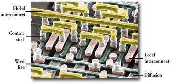
3 Configuration of IC Nitride Oxide PD2 ARC PMD or ILD1 Metal 2, Al Cu W W USG Al Cu Metal 1, Al Cu BPSG PD1 IMD or ILD2 WCVD Sidewall spacer STI n n USG Pwell Pepi Pwafer p p Nwell STI TiN CVD
4 Primary Concerns Deposition Dielectric (oxide, nitride, SiOC, HfO 2 etc. by CVD) Semiconductor (polysi by CVD) Metal (Al, Ti, TiN, Ta, Co, Ni, Cu, Pt, Ru, W by CVD or PVD) Concerned issues Quality (composition, contamination, defect density, mechanical and electrical properties) Uniformity (thickness, conformal step coverage) Filling (via or contact hole)
5 Chemical Vapor Deposition Gases are introduced into the deposition chamber that react and form the desired films on the surface of substrate Reaction take place on the surface instead of in the gas stream (particulates) Sometimes reactants are not available in gaseous form, in which case liquid source may be used. Carrier gas : H 2, N 2, Ar
6 Chemical Vapor Deposition Atmospheric pressure chemical vapor deposition (APCVD) Low pressure chemical vapor deposition (LPCVD) Plasma enhanced chemical vapor deposition (PECVD) Metal organic chemical vapor deposition (MOCVD) Atomic layer chemical vapor deposition (ALCVD) Rapid thermal chemical vapor deposition (RTCVD)
7 Chemical Vapor Deposition 1. Reactant transfer 2. Reactant diffusion 3. Absorption 4. Surface Reaction 5. Desorption of byproducts 6. Byproduct diffusion 7. Byproduct transfer
8 Reaction Mechanisms C G Boundary Layer Gas F 1 F 2 C S Silicon h G : gas phase masstransfer coefficient k s : surfacereaction rate constant F1 = hg( CG CS) F SteadyState = kc 2 s S F1 = F2 k S CS = CG(1 ) hg Growth Rate S 1 F CG kshg ν = = N N k h Number of atoms per cm 3 G Step 2 Step 35
9 Reaction Mechanisms mole fraction in gas phase Y = C C G T Concentration of all molecules in the gas phase SiCl 2H Si 4HCl 4( g) 2( g) ( s) ( g) Y CG PG PG = = = C P P P '... T Total G G Deposition Rate C k h T S G ν = Y N k S h G
10 Refresh: In DealGrove Model DealGrove Relation (linearparabolic growth law): 2 ox T AT = B( t τ ) 2 Tox ox for t >> τ, t >> A 2 /4B = for (t τ) << A 2 /4B T ox Bt Diffusioncontrolled B = ( tτ ) A Reactioncontrolled t ox A, B : temperature, ambient composition, pressure and crystalline orientation τ is related to the initial oxide thickness t Si 0.44 t ox Top oxide surface Silicon Original silicon surface Oxidesilicon surface * DC x Ax i i A= 2 D[ ] B= τ = k h N B s I
11 Dominant Reaction Mechanisms Deposition rate is determined by k s or h G Two limiting cases Surface reaction controlled case Mass transfer controlled case If k s << h G C ν N If h G << k s C ν N T T ky S hy k S limited deposition is VERY temp sensitive. h G limited deposition is VERY geometry (boundary layer) sensitive. G
12 Arrhenius Plot of Growth Rate k S term with k S =k 0 exp(e a /kt) Growth velocity (log scale) Net Growth Velocity h G term with h G =constant Temperature sensitive Mass Transfer Controlled Flow dynamic sensitive Mixed 1/T Reaction Controlled
13 Different precursors. Change h G CVD Si by Different Precursors
14 APCVD k s decreases as the boundary layer thickness increases. Gas depletion along the length of the susceptor. The difficulties of controlling the boundary layer and gas depletion make APCVD typically not a preferable method in furnace batch progress.
15 LPCVD Standup wafers Furnace with resistance heaters Trap Exhaust scrubber Deposition Rate T S G ν = Y N k S h G If many wafers are deposited at once (furnace), operation at the surface reaction controlled region is preferable. Diffusivity is inversely proportional to the number of collisions Diffusivity increases by 100 times as pressure is reduced from 760 to 1torr C k h Vaccum Pump
16 Step Coverage Step coverage is determined by both the arriving angle and precursor surface mobility (sticking coefficient) Sidewall step coverage = b/a Conformity = b/c Bottom step coverage = d/a Overhang = (cb)/b h d w c b Aspect ratio = h/w a Arriving Angle
17 Surface Adsorption Chemisorption & physisorption Binding energy Distance from surface Chemisorbed precursor (bond formation) Low surface mobility Substrate surface Physisorbed precursor (van der Waals or dipoledipole ) High surface mobility
18 Precursor & Adsorption Pyrophoric, toxic, explosive Perfectly symmetrical tetragonal structure neither chemisorb nor physisorb Very Reactive SiH 3, SiH 2, SiH (chemisorption) Low surface mobility overhang H H Si H H
19 Precursor & Adsorption TEOS (tetraethyloxysilane) Not perfectly symmetric due to large size of ethyl group Hydrogen bond physisorb H High surface mobility H H C H H C H H C H C O O Si O H C H C H H O H H H H H C C H H H

20 Step coverage TEOS Silane
21 Void Formation Metal Dielectric Metal Dielectric Void Metal Dielectric
22 Higher current density Void Discontinuous
23 Step Coverage, Pressure and Surface Mobility APCVD (low MFP) No mobility LPCVD (high MFP) No mobility High mobility
24 What is Plasma? Plasma The plasma state is the fourth state of matter. Solid Liquid Gas PLASMA Energy (electricity) Input Gas Flow PLASMA Output Gas Flow Vacuum: to gain enough energy PLASMA: an ionized gas with equal numbers of positive and negative charges. Jyyang in NDL
25 Ionization Ionization: e A 2e A Ionization collisions generate electrons and ions. It sustains the stable plasma. Ionization rate between % 5% Nucleus Nucleus Free Electron Orbital Electron Free Electrons
26 ExcitationRelaxation ExcitationRelaxation: e A e A * A* A hν (Photos) Different atoms or molecules emit different characteristic glow colors. The change of the glow colors is used for the endpoint detection. Grounded electron Excited electron Impact electron hν h: Planck Constant ν: Frequency of Light Excited State Impact electron Nucleus Nucleus hν Ground State
27 Dissociation Dissociation: e AB e A B Electron collides with a molecule, it can break the chemical bond and generate free radicals. Free radicals have at least one unpaired electron and are chemically very reactive. e Free Radicals A B Molecule A B e
28 Sheath Potential x Electrode Bulk plasma Sheath Region V p Electron moves much faster than ions and will charge the electrode (chamber wall) negatively. Sheath Potential Dark space V f
29 Light emission E Plasma Potential Dark space sheath Potential distribution of static plasma Dark space V=0 Free electron Neutrals Ions E wall e A 2 e e A 2 (ionization) e A 2 e A A (dissociation) wall e A 2 2e A A (dissociative ionization) e A 2 e A 2 * (excitation) Plasma: electrons, ions, radicals, atoms, molecules
30 Potential Distribution DC Biased Potential distribution V(x) Cathode (target) Cathode Glow Ar Anode Wafer Cathode Sheath Negative Glow Anode sheath
31 Volt Potential Distribution RF Biased RF Source Plasma Potential DC Bias RF potential Time V V A = A m
32 PECVD Deposition of SiO 2, Si 3 N 4 as Al film has already been on the wafer Al melting point : 660 C <500 C APCVD or LPCVD can be used but will result in poor quality (porous) PECVD is employed Low temperature ( C) Excellent conformal deposition
33 Gas Inlet SiH 4,O 2 PlasmaEnhanced CVD RF power input (13.56MHz) Electrode /Target Glow Discharge Wafers Electrode Heater Vacuum Equal size of electrodes. Electron accelerated by the plasma potential to sustain the plasma. Free radicals are mainly responsible for the deposition.
34 Physical Vapor Deposition transport Gas phase Gas phase Physical Process Only Evaporation Condensation Condensed phase solid Condensed phase solid Vacuum evaporation Sputtering Molecule beam epitaxy
35 Applications: Interconnection
36 Physical Vapor Deposition PVD uses mainly physical process to deposit the films, allowing almost any material deposition Molten source(evaporation) or sputter Usually, PVD operates in a very low pressure environment Surface reaction occurs rapidly and the probability of atoms rearrangement is low Thickness uniformity, shadowing by surface topography, step coverage are challenging issues
37 Thermal Evaporator Wafers Aluminum Charge Aluminum Vapor 10 6 Torr To Pump High Current Source
38 Electron Beam Evaporator Wafers Aluminum Charge 10 6 Torr Aluminum Vapor Electron Beam To Pump Power Supply

39 evaporate Vapor Pressure Vapor pressure for reasonable deposition rate sublime Need to deposit at low pressure to reduce impurities.
40 DC sputter system V(DC) Electrode /Target Glow Discharge Wafers Electrode Heater Gas Inlet Vacuum
41 DC sputter system Potential distribution V(x) Cathode (target) Cathode Glow Ar Anode Wafer Cathode Sheath Negative Glow Anode sheath
42 DC sputter system Al _ Al target Dark space or sheath O e Secondary electron Ar Ar o Ar Al O Ar o Negative glow e Ar e Al Al Al Wafer surface Positive ions are mainly responsible for physical bombardment.
43 DC sputter deposition Target act as electrode,thus source material must be conductive Al, Ti, W Reactive Sputter Deposition Reactive gas can be introduced into system TiN, TiO 2 Controlling stoichiometry is difficult
44 RF Sputter Deposition Since the target is used as an electrode, it should be conductive Otherwise, plasma could not be initiated when the target is nonconductive RF is needed for sputtering oxide, nitride MHz is used
45 RF Sputter Deposition Matching Network RF Generator Wafers Electrode /Target Glow Discharge Electrode Gas Inlet Vacuum Heater
46 Volt Potential Distribution RF Biased RF Source Plasma Potential DC Bias RF potential Time V V A = A m
47 Problem in PVD Technology Overhangs at contact openings Thinner deposition on the sidewall Discontinuous at contact bottom
48 Effect of arrival angle distribution Low MFP: Wide range of arrival angle distribution High MFP: Narrow range of arrival angle distribution
49 Arriving Angles, Contact Holes Larger arriving angle Smaller arriving angle PSG Silicon Nitride
50 Schematic of Magnetron Sputtering Magnets Target Higher plasma density Magnetic field line Erosion grove Right angel between the direction of electric and magnetic field > spiral motion of electrons.
51 PVD vs. CVD CVD: Chemical reaction on the surface PVD: No chemical reaction on the surface CVD: Better step coverage (50% to ~100%) and gap fill capability PVD: Poor step coverage (~ 15%) and gap fill capability PVD: higher quality, purer deposited film, higher conductivity, easy to deposit alloys CVD: always has impurity in the film, lower conductivity, hard to deposit alloys
Chapter 7 Plasma Basic
 Chapter 7 Plasma Basic Hong Xiao, Ph. D. hxiao89@hotmail.com www2.austin.cc.tx.us/hongxiao/book.htm Hong Xiao, Ph. D. www2.austin.cc.tx.us/hongxiao/book.htm 1 Objectives List at least three IC processes
Chapter 7. Plasma Basics
 Chapter 7 Plasma Basics 2006/4/12 1 Objectives List at least three IC processes using plasma Name three important collisions in plasma Describe mean free path Explain how plasma enhance etch and CVD processes
EE143 Fall 2016 Microfabrication Technologies. Lecture 6: Thin Film Deposition Reading: Jaeger Chapter 6
 EE143 Fall 2016 Microfabrication Technologies Lecture 6: Thin Film Deposition Reading: Jaeger Chapter 6 Prof. Ming C. Wu wu@eecs.berkeley.edu 511 Sutardja Dai Hall (SDH) 1 Vacuum Basics Units 1 atmosphere
Plasma Deposition (Overview) Lecture 1
 Lecture 1") Plasma Deposition (Overview) Lecture 1 Material Processes Plasma Processing Plasma-assisted Deposition Implantation Surface Modification Development of Plasma-based processing Microelectronics needs (fabrication
Plasma Deposition (Overview) Lecture 1 Material Processes Plasma Processing Plasma-assisted Deposition Implantation Surface Modification Development of Plasma-based processing Microelectronics needs (fabrication
Film Deposition Part 1
 1 Film Deposition Part 1 Chapter 11 : Semiconductor Manufacturing Technology by M. Quirk & J. Serda Spring Semester 2013 Saroj Kumar Patra Semidonductor Manufacturing Technology, Norwegian University of
CVD: General considerations.
 CVD: General considerations. PVD: Move material from bulk to thin film form. Limited primarily to metals or simple materials. Limited by thermal stability/vapor pressure considerations. Typically requires
Chemical Vapor Deposition (CVD)
") Chemical Vapor Deposition (CVD) source chemical reaction film substrate More conformal deposition vs. PVD t Shown here is 100% conformal deposition ( higher temp has higher surface diffusion) t step 1
Chemical Vapor Deposition (CVD) source chemical reaction film substrate More conformal deposition vs. PVD t Shown here is 100% conformal deposition ( higher temp has higher surface diffusion) t step 1
MICROCHIP MANUFACTURING by S. Wolf
 by S. Wolf Chapter 15 ALUMINUM THIN-FILMS and SPUTTER-DEPOSITION 2004 by LATTICE PRESS CHAPTER 15 - CONTENTS Aluminum Thin-Films Sputter-Deposition Process Steps Physics of Sputter-Deposition Magnetron-Sputtering
Device Fabrication: Etch
 Device Fabrication: Etch 1 Objectives Upon finishing this course, you should able to: Familiar with etch terminology Compare wet and dry etch processes processing and list the main dry etch etchants Become
Fabrication Technology, Part I
 EEL5225: Principles of MEMS Transducers (Fall 2004) Fabrication Technology, Part I Agenda: Microfabrication Overview Basic semiconductor devices Materials Key processes Oxidation Thin-film Deposition Reading:
DEPOSITION OF THIN TiO 2 FILMS BY DC MAGNETRON SPUTTERING METHOD
 Chapter 4 DEPOSITION OF THIN TiO 2 FILMS BY DC MAGNETRON SPUTTERING METHOD 4.1 INTRODUCTION Sputter deposition process is another old technique being used in modern semiconductor industries. Sputtering
EE C245 ME C218 Introduction to MEMS Design Fall 2007
 EE C245 ME C218 Introduction to MEMS Design Fall 2007 Prof. Clark T.-C. Nguyen Dept. of Electrical Engineering & Computer Sciences University of California at Berkeley Berkeley, CA 94720 Lecture 4: Film
Modern Methods in Heterogeneous Catalysis Research: Preparation of Model Systems by Physical Methods
 Modern Methods in Heterogeneous Catalysis Research: Preparation of Model Systems by Physical Methods Methods for catalyst preparation Methods discussed in this lecture Physical vapour deposition - PLD
Lecture 6 Plasmas. Chapters 10 &16 Wolf and Tauber. ECE611 / CHE611 Electronic Materials Processing Fall John Labram 1/68
 Lecture 6 Plasmas Chapters 10 &16 Wolf and Tauber 1/68 Announcements Homework: Homework will be returned to you on Thursday (12 th October). Solutions will be also posted online on Thursday (12 th October)
TMT4320 Nanomaterials November 10 th, Thin films by physical/chemical methods (From chapter 24 and 25)
") 1 TMT4320 Nanomaterials November 10 th, 2015 Thin films by physical/chemical methods (From chapter 24 and 25) 2 Thin films by physical/chemical methods Vapor-phase growth (compared to liquid-phase growth)
1 TMT4320 Nanomaterials November 10 th, 2015 Thin films by physical/chemical methods (From chapter 24 and 25) 2 Thin films by physical/chemical methods Vapor-phase growth (compared to liquid-phase growth)
Semiconductor Technology
 Semiconductor Technology from A to Z Deposition www.halbleiter.org Contents Contents List of Figures II 1 Deposition 1 1.1 Plasma, the fourth aggregation state of a material............. 1 1.1.1 Plasma
Introduction to Plasma
 What is a plasma? The fourth state of matter A partially ionized gas How is a plasma created? Energy must be added to a gas in the form of: Heat: Temperatures must be in excess of 4000 O C Radiation Electric
Introduction to Thin Film Processing
 Introduction to Thin Film Processing Deposition Methods Many diverse techniques available Typically based on three different methods for providing a flux of atomic or molecular material Evaporation Sputtering
Metal Deposition. Filament Evaporation E-beam Evaporation Sputter Deposition
 Metal Deposition Filament Evaporation E-beam Evaporation Sputter Deposition 1 Filament evaporation metals are raised to their melting point by resistive heating under vacuum metal pellets are placed on
Repetition: Practical Aspects
 Repetition: Practical Aspects Reduction of the Cathode Dark Space! E x 0 Geometric limit of the extension of a sputter plant. Lowest distance between target and substrate V Cathode (Target/Source) - +
Chemical Vapor Deposition *
 OpenStax-CNX module: m25495 1 Chemical Vapor Deposition * Andrew R. Barron This work is produced by OpenStax-CNX and licensed under the Creative Commons Attribution License 3.0 note: This module was developed
CHAPTER 6: Etching. Chapter 6 1
 Chapter 6 1 CHAPTER 6: Etching Different etching processes are selected depending upon the particular material to be removed. As shown in Figure 6.1, wet chemical processes result in isotropic etching
Technology for Micro- and Nanostructures Micro- and Nanotechnology
 Lecture 10: Deposition Technology for Micro- and Nanostructures Micro- and Nanotechnology Peter Unger mailto: peter.unger @ uni-ulm.de Institute of Optoelectronics University of Ulm http://www.uni-ulm.de/opto
Section 5: Thin Film Deposition part 1 : sputtering and evaporation. Jaeger Chapter 6. EE143 Ali Javey
 Section 5: Thin Film Deposition part 1 : sputtering and evaporation Jaeger Chapter 6 Vacuum Basics 1. Units 1 atmosphere = 760 torr = 1.013x10 5 Pa 1 bar = 10 5 Pa = 750 torr 1 torr = 1 mm Hg 1 mtorr =
ETCHING Chapter 10. Mask. Photoresist
 ETCHING Chapter 10 Mask Light Deposited Substrate Photoresist Etch mask deposition Photoresist application Exposure Development Etching Resist removal Etching of thin films and sometimes the silicon substrate
Etching Issues - Anisotropy. Dry Etching. Dry Etching Overview. Etching Issues - Selectivity
 Etching Issues - Anisotropy Dry Etching Dr. Bruce K. Gale Fundamentals of Micromachining BIOEN 6421 EL EN 5221 and 6221 ME EN 5960 and 6960 Isotropic etchants etch at the same rate in every direction mask
3.155J/6.152J Microelectronic Processing Technology Fall Term, 2004
 3.155J/6.152J Microelectronic Processing Technology Fall Term, 2004 Bob O'Handley Martin Schmidt Quiz Nov. 17, 2004 Ion implantation, diffusion [15] 1. a) Two identical p-type Si wafers (N a = 10 17 cm
4FNJDPOEVDUPS 'BCSJDBUJPO &UDI
 2010.5.4 1 Major Fabrication Steps in CMOS Process Flow UV light oxygen Silicon dioxide Silicon substrate Oxidation (Field oxide) photoresist Photoresist Coating Mask exposed photoresist Mask-Wafer Exposed
Nanostructure. Materials Growth Characterization Fabrication. More see Waser, chapter 2
 Nanostructure Materials Growth Characterization Fabrication More see Waser, chapter 2 Materials growth - deposition deposition gas solid Physical Vapor Deposition Chemical Vapor Deposition Physical Vapor
E SC 412 Nanotechnology: Materials, Infrastructure, and Safety Wook Jun Nam
 E SC 412 Nanotechnology: Materials, Infrastructure, and Safety Wook Jun Nam Lecture 10 Outline 1. Wet Etching/Vapor Phase Etching 2. Dry Etching DC/RF Plasma Plasma Reactors Materials/Gases Etching Parameters
Combinatorial RF Magnetron Sputtering for Rapid Materials Discovery: Methodology and Applications
 Combinatorial RF Magnetron Sputtering for Rapid Materials Discovery: Methodology and Applications Philip D. Rack,, Jason D. Fowlkes,, and Yuepeng Deng Department of Materials Science and Engineering University
Chapter 3 Engineering Science for Microsystems Design and Fabrication
 Lectures on MEMS and MICROSYSTEMS DESIGN and MANUFACTURE Chapter 3 Engineering Science for Microsystems Design and Fabrication In this Chapter, we will present overviews of the principles of physical and
EE 527 MICROFABRICATION. Lecture 24 Tai-Chang Chen University of Washington
 EE 527 MICROFABRICATION Lecture 24 Tai-Chang Chen University of Washington EDP ETCHING OF SILICON - 1 Ethylene Diamine Pyrocatechol Anisotropy: (100):(111) ~ 35:1 EDP is very corrosive, very carcinogenic,
LECTURE 5 SUMMARY OF KEY IDEAS
 LECTURE 5 SUMMARY OF KEY IDEAS Etching is a processing step following lithography: it transfers a circuit image from the photoresist to materials form which devices are made or to hard masking or sacrificial
UNIVERSITY OF CALIFORNIA. College of Engineering. Department of Electrical Engineering and Computer Sciences. Professor Ali Javey.
 UNIVERSITY OF CALIFORNIA College of Engineering Department of Electrical Engineering and Computer Sciences EE 143 Professor Ali Javey Spring 2009 Exam 2 Name: SID: Closed book. One sheet of notes is allowed.
Repetition: Ion Plating
 Repetition: Ion Plating Substrate HV (bis ca. 1kV) Optional ionization system Source Ionized filling gas Source material, ionized or neutral Repetition: Ion Plating Ion Species Separated ion source Ions
Agenda. 1. Atomic Layer Deposition Technology
 Agenda 1. Atomic Layer Deposition Technology 2. What is ALD? Atomic Layer Deposition is invented in 1977 by T. Suntola et al. - New Deposition Method for Electro-Luminescent Display (ZnS:Mn Thin Films)
Plasma etching. Bibliography
 Plasma etching Bibliography 1. B. Chapman, Glow discharge processes, (Wiley, New York, 1980). - Classical plasma processing of etching and sputtering 2. D. M. Manos and D. L. Flamm, Plasma etching; An
Lecture 1: Vapour Growth Techniques
 PH3EC2 Vapour Growth and Epitaxial Growth Lecturer: Dr. Shinoj V K Lecture 1: Vapour Growth Techniques 1.1 Vapour growth The growth of single crystal materials from the vapour phase. Deposition from the
PHYSICAL VAPOR DEPOSITION OF THIN FILMS
 PHYSICAL VAPOR DEPOSITION OF THIN FILMS JOHN E. MAHAN Colorado State University A Wiley-Interscience Publication JOHN WILEY & SONS, INC. New York Chichester Weinheim Brisbane Singapore Toronto CONTENTS
Ionization Techniques Part IV
 Ionization Techniques Part IV CU- Boulder CHEM 5181 Mass Spectrometry & Chromatography Presented by Prof. Jose L. Jimenez High Vacuum MS Interpretation Lectures Sample Inlet Ion Source Mass Analyzer Detector
Vacuum Technology and film growth. Diffusion Resistor
 Vacuum Technology and film growth Poly Gate pmos Polycrystaline Silicon Source Gate p-channel Metal-Oxide-Semiconductor (MOSFET) Drain polysilicon n-si ion-implanted Diffusion Resistor Poly Si Resistor
Wet and Dry Etching. Theory
 Wet and Dry Etching Theory 1. Introduction Etching techniques are commonly used in the fabrication processes of semiconductor devices to remove selected layers for the purposes of pattern transfer, wafer
PRINCIPLES OF PLASMA DISCHARGES AND MATERIALS PROCESSING
 PRINCIPLES OF PLASMA DISCHARGES AND MATERIALS PROCESSING Second Edition MICHAEL A. LIEBERMAN ALLAN J, LICHTENBERG WILEY- INTERSCIENCE A JOHN WILEY & SONS, INC PUBLICATION CONTENTS PREFACE xrrii PREFACE
Chemistry Instrumental Analysis Lecture 17. Chem 4631
 Chemistry 4631 Instrumental Analysis Lecture 17 Introduction to Optical Atomic Spectrometry From molecular to elemental analysis there are three major techniques used for elemental analysis: Optical spectrometry
Clean-Room microfabrication techniques. Francesco Rizzi Italian Institute of Technology
 Clean-Room microfabrication techniques Francesco Rizzi Italian Institute of Technology Miniaturization The first transistor Miniaturization The first transistor Miniaturization The first transistor Miniaturization
6.5 Optical-Coating-Deposition Technologies
 92 Chapter 6 6.5 Optical-Coating-Deposition Technologies The coating process takes place in an evaporation chamber with a fully controlled system for the specified requirements. Typical systems are depicted
Solutions for Assignment-6
 Solutions for Assignment-6 Q1. What is the aim of thin film deposition? [1] (a) To maintain surface uniformity (b) To reduce the amount (or mass) of light absorbing materials (c) To decrease the weight
Lecture 10 Thin Film Growth
 Lecture 10 Thin Film Growth 1/76 Announcements Homework: Homework Number 2 is returned today, please pick it up from me at the end of the class. Solutions are online. Homework 3 will be set Thursday (2
Step Coverage by ALD Films: Theory and Examples
 Step Coverage by ALD Films: Theory and Examples of Ideal and Non-Ideal Reactions Roy G. Gordon Cambridge, MA 1 L Step Coverage in Holes with High Aspect Ratio Step coverage = (b/a) x 100% a Aspect ratio
Section 3: Etching. Jaeger Chapter 2 Reader
 Section 3: Etching Jaeger Chapter 2 Reader Etch rate Etch Process - Figures of Merit Etch rate uniformity Selectivity Anisotropy d m Bias and anisotropy etching mask h f substrate d f d m substrate d f
Chapter 9, Etch. Hong Xiao, Ph. D. www2.austin.cc.tx.us/hongxiao/book.htm
 Chapter 9, Etch Hong Xiao, Ph. D. hxiao89@hotmail.com www2.austin.cc.tx.us/hongxiao/book.htm Hong Xiao, Ph. D. www2.austin.cc.tx.us/hongxiao/book.htm 1 Objectives Upon finishing this course, you should
Lecture 10. Vacuum Technology and Plasmas Reading: Chapter 10. ECE Dr. Alan Doolittle
 Lecture 10 Vacuum Technology and Plasmas Reading: Chapter 10 Vacuum Science and Plasmas In order to understand deposition techniques such as evaporation, sputtering,, plasma processing, chemical vapor
Self-study problems and questions Processing and Device Technology, FFF110/FYSD13
 Self-study problems and questions Processing and Device Technology, FFF110/FYSD13 Version 2016_01 In addition to the problems discussed at the seminars and at the lectures, you can use this set of problems
Etching: Basic Terminology
 Lecture 7 Etching Etching: Basic Terminology Introduction : Etching of thin films and sometimes the silicon substrate are very common process steps. Usually selectivity, and directionality are the first
Lecture 15 Etching. Chapters 15 & 16 Wolf and Tauber. ECE611 / CHE611 Electronic Materials Processing Fall John Labram 1/76
 Lecture 15 Etching Chapters 15 & 16 Wolf and Tauber 1/76 Announcements Term Paper: You are expected to produce a 4-5 page term paper on a selected topic (from a list). Term paper contributes 25% of course
FRAUNHOFER IISB STRUCTURE SIMULATION
 FRAUNHOFER IISB STRUCTURE SIMULATION Eberhard Bär eberhard.baer@iisb.fraunhofer.de Page 1 FRAUNHOFER IISB STRUCTURE SIMULATION Overview SiO 2 etching in a C 2 F 6 plasma Ga ion beam sputter etching Ionized
SCALING OF HOLLOW CATHODE MAGNETRONS FOR METAL DEPOSITION a)
") SCALING OF HOLLOW CATHODE MAGNETRONS FOR METAL DEPOSITION a) Gabriel Font b) Novellus Systems, Inc. San Jose, CA, 95134 USA and Mark J. Kushner Dept. of Electrical and Computer Engineering Urbana, IL,
SCALING OF HOLLOW CATHODE MAGNETRONS FOR METAL DEPOSITION a) Gabriel Font b) Novellus Systems, Inc. San Jose, CA, 95134 USA and Mark J. Kushner Dept. of Electrical and Computer Engineering Urbana, IL,
UNIT 3. By: Ajay Kumar Gautam Asst. Prof. Dev Bhoomi Institute of Technology & Engineering, Dehradun
 UNIT 3 By: Ajay Kumar Gautam Asst. Prof. Dev Bhoomi Institute of Technology & Engineering, Dehradun 1 Syllabus Lithography: photolithography and pattern transfer, Optical and non optical lithography, electron,
Secondary ion mass spectrometry (SIMS)
") Secondary ion mass spectrometry (SIMS) ELEC-L3211 Postgraduate Course in Micro and Nanosciences Department of Micro and Nanosciences Personal motivation and experience on SIMS Offers the possibility to
Secondary ion mass spectrometry (SIMS) ELEC-L3211 Postgraduate Course in Micro and Nanosciences Department of Micro and Nanosciences Personal motivation and experience on SIMS Offers the possibility to
Atmospheric pressure Plasma Enhanced CVD for large area deposition of TiO 2-x electron transport layers for PV. Heather M. Yates
 Atmospheric pressure Plasma Enhanced CVD for large area deposition of TiO 2-x electron transport layers for PV Heather M. Yates Why the interest? Perovskite solar cells have shown considerable promise
Thin Film Deposition
 Thin Film Deposition Physical processes Evaporation: Thermal, E-beam, Laser, Ion-plating. Sputtering: DC, RF, Magnetron, Reactive. Spray: Flame, Plasma. Chemical processes Chemical Vapor Deposition (CVD):
Pulsed Laser Deposition; laser ablation. Final apresentation for TPPM Diogo Canavarro, MEFT
 Pulsed Laser Deposition; laser ablation Final apresentation for TPPM Diogo Canavarro, 56112 MEFT Summary What is PLD? What is the purpose of PLD? How PLD works? Experimental Setup Processes in PLD The
Lecture 11. Etching Techniques Reading: Chapter 11. ECE Dr. Alan Doolittle
 Lecture 11 Etching Techniques Reading: Chapter 11 Etching Techniques Characterized by: 1.) Etch rate (A/minute) 2.) Selectivity: S=etch rate material 1 / etch rate material 2 is said to have a selectivity
MODELING OF SEASONING OF REACTORS: EFFECTS OF ION ENERGY DISTRIBUTIONS TO CHAMBER WALLS*
 MODELING OF SEASONING OF REACTORS: EFFECTS OF ION ENERGY DISTRIBUTIONS TO CHAMBER WALLS* Ankur Agarwal a) and Mark J. Kushner b) a) Department of Chemical and Biomolecular Engineering University of Illinois,
Dry Etching Zheng Yang ERF 3017, MW 5:15-6:00 pm
 Dry Etching Zheng Yang ERF 3017, email: yangzhen@uic.edu, MW 5:15-6:00 pm Page 1 Page 2 Dry Etching Why dry etching? - WE is limited to pattern sizes above 3mm - WE is isotropic causing underetching -
Surface processes during thin-film growth
 Plasma Sources Sci. Technol. 9 (2000) 455 467. Printed in the UK PII: S0963-0252(00)15187-4 Surface processes during thin-film growth Achim von Keudell Max-Planck-Institut für Plasmaphysik, Boltzmannstrasse
Lecture 150 Basic IC Processes (10/10/01) Page ECE Analog Integrated Circuits and Systems P.E. Allen
 Page ECE Analog Integrated Circuits and Systems P.E. Allen") Lecture 150 Basic IC Processes (10/10/01) Page 1501 LECTURE 150 BASIC IC PROCESSES (READING: TextSec. 2.2) INTRODUCTION Objective The objective of this presentation is: 1.) Introduce the fabrication of
Lecture 150 Basic IC Processes (10/10/01) Page 1501 LECTURE 150 BASIC IC PROCESSES (READING: TextSec. 2.2) INTRODUCTION Objective The objective of this presentation is: 1.) Introduce the fabrication of
Plasma Chemistry Study in an Inductively Coupled Dielectric Etcher
 Plasma Chemistry Study in an Inductively Coupled Dielectric Etcher Chunshi Cui, John Trow, Ken Collins, Betty Tang, Luke Zhang, Steve Shannon, and Yan Ye Applied Materials, Inc. October 26, 2000 10/28/2008
Reactive Ion Etching (RIE)
") Reactive Ion Etching (RIE) RF 13.56 ~ MHz plasma Parallel-Plate Reactor wafers Sputtering Plasma generates (1) Ions (2) Activated neutrals Enhance chemical reaction 1 2 Remote Plasma Reactors Plasma Sources
Reactive Ion Etching (RIE) RF 13.56 ~ MHz plasma Parallel-Plate Reactor wafers Sputtering Plasma generates (1) Ions (2) Activated neutrals Enhance chemical reaction 1 2 Remote Plasma Reactors Plasma Sources
Carbon Nanotubes in Interconnect Applications
 Carbon Nanotubes in Interconnect Applications Page 1 What are Carbon Nanotubes? What are they good for? Why are we interested in them? - Interconnects of the future? Comparison of electrical properties
Fabrication and Characterization of Silicon Rich Oxide (SRO) Thin Film Deposited by Plasma Enhanced CVD for Si Quantum Dot
 Thin Film Deposited by Plasma Enhanced CVD for Si Quantum Dot") Fabrication and Characterization of Silicon Rich Oxide (SRO) Thin Film Deposited by Plasma Enhanced CVD for Si Quantum Dot By Tian Zhang School of Photovoltaic and Renewable Energy Engineering Technology
Fabrication and Characterization of Silicon Rich Oxide (SRO) Thin Film Deposited by Plasma Enhanced CVD for Si Quantum Dot By Tian Zhang School of Photovoltaic and Renewable Energy Engineering Technology
Chemistry Instrumental Analysis Lecture 34. Chem 4631
 Chemistry 4631 Instrumental Analysis Lecture 34 From molecular to elemental analysis there are three major techniques used for elemental analysis: Optical spectrometry Mass spectrometry X-ray spectrometry
-- DEPOSITION INTERVAL
 United States Patent (19) Sukjarev 54) PLASMA-ENHANCED OXIDE PROCESS OPTIMIZATION AND MATERIAL AND APPARATUS THEREFOR 75 Inventor: Valeriy Y. Sukjarev, Cupertino, Calif. 73 Assignee: LSI Logic Corporation,
Chapter 3: Thin film deposition and characterization techniques
 Chapter 3: Thin film deposition and characterization techniques 3.1 Introduction: The Material Science and Engineering community s ability to visualize the novel materials with extraordinary combination
Application of Rarefied Flow & Plasma Simulation Software
 2016/5/18 Application of Rarefied Flow & Plasma Simulation Software Yokohama City in Japan Profile of Wave Front Co., Ltd. Name : Wave Front Co., Ltd. Incorporation : March 1990 Head Office : Yokohama
Ajay Kumar Gautam Asst. Prof. Electronics & Communication Engineering Dev Bhoomi Institute of Technology & Engineering Dehradun UNIT II
 Ajay Kumar Gautam Asst. Prof. Electronics & Communication Engineering Dev Bhoomi Institute of Technology & Engineering Dehradun UNIT II Syllabus EPITAXIAL PROCESS: Epitaxy and its concept, Growth kinetics
Photovoltaic cell and module physics and technology. Vitezslav Benda, Prof Czech Technical University in Prague
 Photovoltaic cell and module physics and technology Vitezslav Benda, Prof Czech Technical University in Prague benda@fel.cvut.cz www.fel.cvut.cz 1 Outlines Photovoltaic Effect Photovoltaic cell structure
Electrical Discharges Characterization of Planar Sputtering System
 International Journal of Recent Research and Review, Vol. V, March 213 ISSN 2277 8322 Electrical Discharges Characterization of Planar Sputtering System Bahaa T. Chaid 1, Nathera Abass Ali Al-Tememee 2,
Photovoltaic cell and module physics and technology
 Photovoltaic cell and module physics and technology Vitezslav Benda, Prof Czech Technical University in Prague benda@fel.cvut.cz www.fel.cvut.cz 6/21/2012 1 Outlines Photovoltaic Effect Photovoltaic cell
Effect of Spiral Microwave Antenna Configuration on the Production of Nano-crystalline Film by Chemical Sputtering in ECR Plasma
 THE HARRIS SCIENCE REVIEW OF DOSHISHA UNIVERSITY, VOL. 56, No. 1 April 2015 Effect of Spiral Microwave Antenna Configuration on the Production of Nano-crystalline Film by Chemical Sputtering in ECR Plasma
EE-612: Lecture 22: CMOS Process Steps
 EE-612: Lecture 22: CMOS Process Steps Mark Lundstrom Electrical and Computer Engineering Purdue University West Lafayette, IN USA Fall 2006 NCN www.nanohub.org Lundstrom EE-612 F06 1 outline 1) Unit Process
EE 527 MICROFABRICATION. Lecture 25 Tai-Chang Chen University of Washington
 EE 527 MICROFABRICATION Lecture 25 Tai-Chang Chen University of Washington ION MILLING SYSTEM Kaufmann source Use e-beam to strike plasma A magnetic field applied to increase ion density Drawback Low etch
Lecture 3 Vacuum Science and Technology
 Lecture 3 Vacuum Science and Technology Chapter 3 - Wolf and Tauber 1/56 Announcements Homework will be online from noon today. This is homework 1 of 4. 25 available marks (distributed as shown). This
2.1 Template Method Microemulsion Nanostructured Polymer (Copolymer, DNA) Nanostructured Ceramics (AAO, Porous Silica, Zeolite)
 Nanostructured Ceramics (AAO, Porous Silica, Zeolite)") Chapter 1. Characteristics of Nanomaterials Chapter 2. Methodology of Nanomaterials 2.1 Template Method 2.1.1. Microemulsion 2.1.2. Nanostructured Polymer (Copolymer, DNA) 2.1.3. Nanostructured Ceramics
Chapter 1. Characteristics of Nanomaterials Chapter 2. Methodology of Nanomaterials 2.1 Template Method 2.1.1. Microemulsion 2.1.2. Nanostructured Polymer (Copolymer, DNA) 2.1.3. Nanostructured Ceramics
VACUUM TECHNOLOGIES NEEDED FOR 3D DEVICE PROCESSING
 VACUUM TECHNOLOGIES NEEDED FOR 3D DEVICE PROCESSING Future ICs will use more 3D device structures such as finfets and gate-all-around (GAA) transistors, and so vacuum deposition processes are needed that
Harris: Quantitative Chemical Analysis, Eight Edition CHAPTER 23: GAS CHROMATOGRAPHY
 Harris: Quantitative Chemical Analysis, Eight Edition CHAPTER 23: GAS CHROMATOGRAPHY Chapter 23. Gas Chromatography What did they eat in the year 1,000? GC of Cholesterol and other lipids extracted from
HONOUR SCHOOL OF NATURAL SCIENCE. Final Examination GENERAL PHYSICAL CHEMISTRY I. Answer FIVE out of nine questions
 HONOUR SCHOOL OF NATURAL SCIENCE Final Examination GENERAL PHYSICAL CHEMISTRY I Monday, 12 th June 2000, 9.30 a.m. - 12.30 p.m. Answer FIVE out of nine questions The numbers in square brackets indicate
Physical Vapor Deposition
 Physical Vapor Deposition EVAPORATION SPUTTERING Typically used for metallization of semiconductors. Both Evaporation & Sputtering are done in vacuum environments. Typically: y Evaporation Pressures are
Secondary Ion Mass Spectroscopy (SIMS)
") Secondary Ion Mass Spectroscopy (SIMS) Analyzing Inorganic Solids * = under special conditions ** = semiconductors only + = limited number of elements or groups Analyzing Organic Solids * = under special
Secondary Ion Mass Spectroscopy (SIMS) Analyzing Inorganic Solids * = under special conditions ** = semiconductors only + = limited number of elements or groups Analyzing Organic Solids * = under special
Document Version Publisher s PDF, also known as Version of Record (includes final page, issue and volume numbers)
") The effect of ion-surface and ion-bulk interactions during hydrogenated amorphous silicon deposition Smets, A.H.M.; Kessels, W.M.M.; van de Sanden, M.C.M. Published in: Journal of Applied Physics DOI:
The effect of ion-surface and ion-bulk interactions during hydrogenated amorphous silicon deposition Smets, A.H.M.; Kessels, W.M.M.; van de Sanden, M.C.M. Published in: Journal of Applied Physics DOI:
CHEMICAL VAPOR DEPOSITION (CVD)
") CHEMICAL VAPOR DEPOSITION (CVD) A process of formation of a non-volatile solid film on a substrate from the reaction of vapor phase chemical reactants containing the right proportion of constituents. ELEMETRY
CHEMICAL VAPOR DEPOSITION (CVD) A process of formation of a non-volatile solid film on a substrate from the reaction of vapor phase chemical reactants containing the right proportion of constituents. ELEMETRY
Chapter 3 Basics Semiconductor Devices and Processing
 Chapter 3 Basics Semiconductor Devices and Processing Hong Xiao, Ph. D. www2.austin.cc.tx.us/hongxiao/book.htm Hong Xiao, Ph. D. www2.austin.cc.tx.us/hongxiao/book.htm 1 Objectives Identify at least two
SPUTTER-WIND HEATING IN IONIZED METAL PVD+
 SPUTTER-WIND HEATING IN IONIZED METAL PVD+ Junqing Lu* and Mark Kushner** *Department of Mechanical and Industrial Engineering **Department of Electrical and Computer Engineering University of Illinois
Repetition: Physical Deposition Processes
 Repetition: Physical Deposition Processes PVD (Physical Vapour Deposition) Evaporation Sputtering Diode-system Triode-system Magnetron-system ("balanced/unbalanced") Ion beam-system Ionplating DC-glow-discharge
Extrel Application Note
 Extrel Application Note Real-Time Plasma Monitoring and Detection of Trace H 2 O and HF Species in an Argon Based Plasma Jian Wei, 575 Epsilon Drive, Pittsburgh, PA 15238. (Presented at the 191st Electrochemical
Hydrogenation of Single Walled Carbon Nanotubes
 Hydrogenation of Single Walled Carbon Nanotubes Anders Nilsson Stanford Synchrotron Radiation Laboratory (SSRL) and Stockholm University Coworkers and Ackowledgement A. Nikitin 1), H. Ogasawara 1), D.
Previous Lecture. Electron beam lithoghraphy e - Electrons are generated in vacuum. Electron beams propagate in vacuum
 Previous Lecture Electron beam lithoghraphy e - Electrons are generated in vacuum Electron beams propagate in vacuum Lecture 6: Vacuum & plasmas Objectives From this vacuum lecture you will learn: What
Taurus-Topography. Topography Modeling for IC Technology
 SYSTEMS PRODUCTS LOGICAL PRODUCTS PHYSICAL IMPLEMENTATION SIMULATION AND ANALYSIS LIBRARIES TCAD Aurora DFM WorkBench Davinci Medici Raphael Raphael-NES Silicon Early Access TSUPREM-4 Taurus-Device Taurus-Lithography
CHAPTER 3: Epitaxy. City University of Hong Kong
 1 CHAPTER 3: Epitaxy Epitaxy (epi means "upon" and taxis means "ordered") is a term applied to processes used to grow a thin crystalline layer on a crystalline substrate. The seed crystal in epitaxial