Quantum Nano-Engineering Lab
|
|
|
- Phebe Byrd
- 6 years ago
- Views:
Transcription


1 Quantum Nano-Engineering Quantum Lab Engineering Lab 12/29/2014


2 Many thanks to Our Group: Dr. Shira Yochelis, Eyal Cohen, Eran Katzir, Avner Neubauer, Guy Koplovitz, Oren Ben Dor, Ido Eisnberg, Ohad Westrich, Matan Galanty. Nir Peer, Chen Alpern; Amir Ziv, Aviya Perlman Illouz, Kuti Uliel And Grzegorz Jung Physics department, Ben Gurion University Beer Sheva Israel Ron Naaman Department of Chemical Physics, Weizmann Institute, Rehovot 76100, Israel Nadav Katz, Yaov Kalcheim, Oded Millo, Racah Institute of Physics, Hebrew University, Jerusalem 91904, Israel Uri Banin Department of physical chemistry, Hebrew University, Jerusalem 91904, Israel 2 Financing:, ISF, ISF-BICORA, DARPA, MOD, Israel Taiwan, Magneton Capital Nature, FTA, Peter Brojde center, Volkswagen, Leverhulme

 CISS based")
3 Lecture Synopsis Quantum effects at room temperature? Chiral induced spin selectivity effect (CISS) CISS based devices E F Au 3


4 Toward RT Quantum Machines Implementation of devices room temperatures quantum Room temperature quantum coherence Very hard to achieve but we can use a mix of quantum and classical approach Meeting between Top-down to Bottom -up Controlled Coupling 4


5 Spin Electronics Electrons have charge and spin 1/2 Conventional electronic devices ignore the spin property and rely strictly on the transport of the electrical charge of electrons Adding the spin degree of freedom provides new effects, new capabilities and new functionalities 5

6 Why Spin? Energy and heat- For Spintronics, less energy Quantum effects -It may be a way for introducing the spin properties to our tool arsenal. 6


7 Spintronics Devices The 2007 Nobel Prize in Physics was awarded to : Albert Fert and Peter Grünberg for the discovery of GMR 7


8 Chiral based spintronics 8
9 What do we have to contribute Simple and easy to process Small Cheep Si compatible From industrial point of view lets take existing magnetic devices and improve them with our CISS effect 9


10 10 SOC is the main cause for CISS 10

11 The CISS effect The CISS effect- Chiral induced Spin Selectivity. S P S P 11


12 Transport Vs Optics Chirality Induced Spin-selectivity (CISS) effect SC NCs Chiral Molecules FM E F E F M z 12 12
.")
13 . Spin dependent transport through double stranded DNA Chiral Induced Spin Selectivity - CISS Zuoti Xie, Tal Markus, Sidney Cohen, Zeev Vager, Rafael Gutierrez, Nano Letters, 11, (2011). Current (na) bp 40 bp 50 bp 40 bp On Au V o ltage (V ) di/dv 26 bp 40 bp 50 bp 40 bp On Au V o ltage (V ) 13


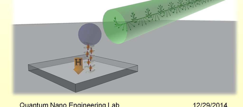
14 Magnetic Memory without a Magnet 14


15 Memory devices Fast but need constant power DRAM - Dynamic random-access memory refreshed periodically Slow last for 10 years Flesh memory SRAM- Static random-access memory Does not need to be periodically refreshed All existing memory technologies challenged when critical size is smaller than 45 nm We want: No constant power, long lived, fast, standard technology 15


16 The Charily Molecular based Universal memory Fast Dense Non- Volatile Power efficient nm size transport Unit size 10nm stable No back scattering The industry needs are met without compromising in cost, compatibility to standard Si process & complexity of design 16
17 Method Sample Preparation Pre-adsorption Optical lithography Adsorption 1/5/10mM on 40x50 um 2 adsorption areas Post-adsorption Al 2 O 3 is evaporated in two sessions: 4-5nm followed by 2nm reduces pinholes Evaporation of Ni 30nm SiO2 (PECVD) SiO2 Si 17

. (a) (b) 18")
18 Si based CISS devices Low-power silicon based spintronic transistors with chiral molecular spin filter Potential difficulty- pin-holes in the organic monolayer. The problem was solved by evaporating thin layer (3-5 nm) of AlOx on top of the organic monolayer. Nature Communications 4, 2256 DOI: (2013). (a) (b) 18
19 Memory writing at low temperatures Nature Communications 4, 2256 DOI: (2013). Highlighted in Nature "Nanotechnology: A memory device with a twist" search/highlight/8613 Magnetization of the device at 2K 19


20 Dual direction writing Spin filter not spin polarizer? E F Au 20
21 Memory effect on a Real Device Nature Communications 4, 2256 DOI: (2013). Highlighted in Nature "Nanotechnology: A memory device with a twist" search/highlight/8613 Memory effect. Writing the at -15V reading at lower voltage. For the same direction of current the resistance is high and low for the opposite direction of current 21 Breakthrough in memory technologies could bring faster computing, smaller memory device -

22 22


 500n m")

23 Methods 5 µm nm Ni-based Hall effect device (anomalous HE) 500n m 532nm Circular Polarized Beam 23 23
24 Calibration BzI x n = V te n n xy experiment theory ~ 10 electrons / Meter 27 3 ~ 5 10 electrons / Meter 26 3 t B (t) 24 Paper under review 24

25 Optical CISS Comparing the right hand circular polarization and left hand circular polarization with the same linear polarization One order of magnitude difference Spin detector
26 Results Nano letters 2014 Dark Light Dark Light 26 26

 (2012) Paper")
27 Results Dark Light Dark Light 27 Li Ye et al. Physical Review B 85, (R) (2012) Paper under review 27


28 Methods Highly localized magnetization device (measured with MFM) 532nm Circular Polarized Beam 5nm Au 1.5nm Co 28 28


29 Results Nano letters 2014 Illuminated area in illuminated sample Unilluminated area in illuminated sample Illuminated area in reference sample (no Molecules & no NC) 29 29
30 CISS Future Applications Magnetic memory Source Gate Drain Spin transistors 3D spin logic Contact 3 Ferromagnetic Electrical gating A scheme of the XOR MSM device Ferromagnetic nano structure Local EMR Chiral R Contact 1 Chiral S Contact 2 30


31 Changing the world of memory device as we know 31
Quantum Nano-Engineering Lab
 30.11.14 1 Quantum Nano-Engineering Quantum Lab Engineering Lab 10/23/2015 Many thanks to Our Group: Dr. Shira Yochelis, Eyal Cohen, Eran Katzir, Avner Neubauer, Guy Koplovitz, Oren Ben Dor, Ido Eisnberg,
L a b. Quantum Nano Engineering Lab 10/17/ Quantum Nano-Engineering Lab
 1 Quantum Nano-Engineering Lab Jerusalem and The Hebrew University Inauguration ceremony 1925 The Hebrew University of Jerusalem is Israel's oldest (1925) university. The First Board of Governors included
Proximity Effect in Hybrid Superconducting/Organic molecule nano particle system
 Proximity Effect in Hybrid Superconducting/Organic molecule nano particle system Yossi Paltiel Applied Physics Department Center for nano science and nano technology, HUJI, Israel Oded Millo Nadav Katz
TRANSVERSE SPIN TRANSPORT IN GRAPHENE
 International Journal of Modern Physics B Vol. 23, Nos. 12 & 13 (2009) 2641 2646 World Scientific Publishing Company TRANSVERSE SPIN TRANSPORT IN GRAPHENE TARIQ M. G. MOHIUDDIN, A. A. ZHUKOV, D. C. ELIAS,
From Hall Effect to TMR
 From Hall Effect to TMR 1 Abstract This paper compares the century old Hall effect technology to xmr technologies, specifically TMR (Tunnel Magneto-Resistance) from Crocus Technology. It covers the various
Fundamental concepts of spintronics
 Fundamental concepts of spintronics Jaroslav Fabian Institute for Theoretical Physics University of Regensburg Stara Lesna, 24. 8. 2008 SFB 689 :outline: what is spintronics? spin injection spin-orbit
From nanophysics research labs to cell phones. Dr. András Halbritter Department of Physics associate professor
 From nanophysics research labs to cell phones Dr. András Halbritter Department of Physics associate professor Curriculum Vitae Birth: 1976. High-school graduation: 1994. Master degree: 1999. PhD: 2003.
Nanoimprint Lithography
 Nanoimprint Lithography Wei Wu Quantum Science Research Advanced Studies HP Labs, Hewlett-Packard Email: wei.wu@hp.com Outline Background Nanoimprint lithography Thermal based UV-based Applications based
Spintronics. Kishan K. Sinha. Xiaoshan Xu s Group Department of Physics and Astronomy University of Nebraska-Lincoln
 Spintronics by Kishan K. Sinha Xiaoshan Xu s Group Department of Physics and Astronomy University of Nebraska-Lincoln What is spintronics? In conventional electronics, motion of electrons is controlled
A Review of Spintronics based Data Storage. M.Tech Student Professor
 A Review of Spintronics based Data Storage By: Mohit P. Tahiliani S. Vadakkan M.Tech Student Professor NMAMIT, Nitte NMAMIT, Nitte CONTENTS Introduction Giant Magneto Resistance (GMR) Tunnel Magneto Resistance
Introduction to Spintronics and Spin Caloritronics. Tamara Nunner Freie Universität Berlin
 Introduction to Spintronics and Spin Caloritronics Tamara Nunner Freie Universität Berlin Outline Format of seminar How to give a presentation How to search for scientific literature Introduction to spintronics
MolNanoSpin: Spintronique moléculaire avec des molécules-aimants
 MolNanoSpin: Spintronique moléculaire avec des molécules-aimants W. Wernsdorfer : Institut Néel T. Mallah : Institut de Chimie Moléculaire et des Matériaux d'orsay P. Mialane : Institut Lavoisier Journées
Challenges for Materials to Support Emerging Research Devices
 Challenges for Materials to Support Emerging Research Devices C. Michael Garner*, James Hutchby +, George Bourianoff*, and Victor Zhirnov + *Intel Corporation Santa Clara, CA + Semiconductor Research Corporation
Author : Fabrice BERNARD-GRANGER September 18 th, 2014
 Author : September 18 th, 2014 Spintronic Introduction Spintronic Design Flow and Compact Modelling Process Variation and Design Impact Semiconductor Devices Characterisation Seminar 2 Spintronic Introduction
Saroj P. Dash. Chalmers University of Technology. Göteborg, Sweden. Microtechnology and Nanoscience-MC2
 Silicon Spintronics Saroj P. Dash Chalmers University of Technology Microtechnology and Nanoscience-MC2 Göteborg, Sweden Acknowledgement Nth Netherlands University of Technology Sweden Mr. A. Dankert Dr.
Giant Magnetoresistance
 Giant Magnetoresistance Zachary Barnett Course: Solid State II; Instructor: Elbio Dagotto; Semester: Spring 2008 Physics Department, University of Tennessee (Dated: February 24, 2008) This paper briefly
Spintronics. Seminar report SUBMITTED TO: SUBMITTED BY:
 A Seminar report On Spintronics Submitted in partial fulfillment of the requirement for the award of degree of Electronics SUBMITTED TO: SUBMITTED BY: www.studymafia.org www.studymafia.org Preface I have
Advanced Topics In Solid State Devices EE290B. Will a New Milli-Volt Switch Replace the Transistor for Digital Applications?
 Advanced Topics In Solid State Devices EE290B Will a New Milli-Volt Switch Replace the Transistor for Digital Applications? August 28, 2007 Prof. Eli Yablonovitch Electrical Engineering & Computer Sciences
Introduction to Quantum Dynamics and Control
 EE 290O. Advanced Topics in Control: Introduction to Quantum Dynamics and Control Instructor: Alireza Shabani Contact : shabani@berkeley.edu Office: Gilman, Room 19 Cory 278 Office Hours: Wednesdays 3-4
X-Ray Spectro-Microscopy Joachim Stöhr Stanford Synchrotron Radiation Laboratory
 X-Ray Spectro-Microscopy Joachim Stöhr Stanford Synchrotron Radiation Laboratory X-Rays have come a long way Application to Magnetic Systems 1 µm 1895 1993 2003 http://www-ssrl.slac.stanford.edu/stohr/index.htm
CSCB58:Computer Organization
 CSC58:Computer Organization Instructor: rian Harrington brian.harrington@utsc.utoronto.ca * Original slides by Steve Engels Why take CSC58? To better understand computers! See what's going on "under the
ConceptGraphene. Small or medium-scale focused research project. WP4 Spin transport devices
 ConceptGraphene New Electronics Concept: Wafer-Scale Epitaxial Graphene Small or medium-scale focused research project WP4 Spin transport devices Deliverable 4.1 Report on spin transport in graphene on
MRAM: Device Basics and Emerging Technologies
 MRAM: Device Basics and Emerging Technologies Matthew R. Pufall National Institute of Standards and Technology 325 Broadway, Boulder CO 80305-3337 Phone: +1-303-497-5206 FAX: +1-303-497-7364 E-mail: pufall@boulder.nist.gov
Thin Film Transistors (TFT)
") Thin Film Transistors (TFT) a-si TFT - α-si:h (Hydrogenated amorphous Si) deposited with a PECVD system (low temp. process) replaces the single crystal Si substrate. - Inverted staggered structure with
Thin Film Transistors (TFT) a-si TFT - α-si:h (Hydrogenated amorphous Si) deposited with a PECVD system (low temp. process) replaces the single crystal Si substrate. - Inverted staggered structure with
Wouldn t it be great if
 IDEMA DISKCON Asia-Pacific 2009 Spin Torque MRAM with Perpendicular Magnetisation: A Scalable Path for Ultra-high Density Non-volatile Memory Dr. Randall Law Data Storage Institute Agency for Science Technology
Graphene photodetectors with ultra-broadband and high responsivity at room temperature
 SUPPLEMENTARY INFORMATION DOI: 10.1038/NNANO.2014.31 Graphene photodetectors with ultra-broadband and high responsivity at room temperature Chang-Hua Liu 1, You-Chia Chang 2, Ted Norris 1.2* and Zhaohui
Page 1. A portion of this study was supported by NEDO.
 MRAM : Materials and Devices Current-induced Domain Wall Motion High-speed MRAM N. Ishiwata NEC Corporation Page 1 A portion of this study was supported by NEDO. Outline Introduction Positioning and direction
single-electron electron tunneling (SET)
") single-electron electron tunneling (SET) classical dots (SET islands): level spacing is NOT important; only the charging energy (=classical effect, many electrons on the island) quantum dots: : level spacing
single-electron electron tunneling (SET) classical dots (SET islands): level spacing is NOT important; only the charging energy (=classical effect, many electrons on the island) quantum dots: : level spacing
Integrating MEMS Electro-Static Driven Micro-Probe and Laser Doppler Vibrometer for Non-Contact Vibration Mode SPM System Design
 Tamkang Journal of Science and Engineering, Vol. 12, No. 4, pp. 399 407 (2009) 399 Integrating MEMS Electro-Static Driven Micro-Probe and Laser Doppler Vibrometer for Non-Contact Vibration Mode SPM System
Session Chair: Prof. Haiping Cheng (University of Florida) Dr. Lei Shen. National University of Singapore
 Dr. Lei Shen. National University of Singapore") B1. Modeling Quantum Transport at Nanoscale Chair(s): Chun ZHANG, National University of Singapore, Singapore Session s Title (if available) Tue - 17 Jan 2017 13:00 ~ 14:30 Room 2 Session Chair: Prof.
B1. Modeling Quantum Transport at Nanoscale Chair(s): Chun ZHANG, National University of Singapore, Singapore Session s Title (if available) Tue - 17 Jan 2017 13:00 ~ 14:30 Room 2 Session Chair: Prof.
Intrinsic Electronic Transport Properties of High. Information
 Intrinsic Electronic Transport Properties of High Quality and MoS 2 : Supporting Information Britton W. H. Baugher, Hugh O. H. Churchill, Yafang Yang, and Pablo Jarillo-Herrero Department of Physics, Massachusetts
EE141- Fall 2002 Lecture 27. Memory EE141. Announcements. We finished all the labs No homework this week Projects are due next Tuesday 9am EE141
 - Fall 2002 Lecture 27 Memory Announcements We finished all the labs No homework this week Projects are due next Tuesday 9am 1 Today s Lecture Memory:» SRAM» DRAM» Flash Memory 2 Floating-gate transistor
Ferromagnetism and Anomalous Hall Effect in Graphene
 Ferromagnetism and Anomalous Hall Effect in Graphene Jing Shi Department of Physics & Astronomy, University of California, Riverside Graphene/YIG Introduction Outline Proximity induced ferromagnetism Quantized
Advanced Lab Course. Tunneling Magneto Resistance
 Advanced Lab Course Tunneling Magneto Resistance M06 As of: 015-04-01 Aim: Measurement of tunneling magnetoresistance for different sample sizes and recording the TMR in dependency on the voltage. Content
Moores Law for DRAM. 2x increase in capacity every 18 months 2006: 4GB
 MEMORY Moores Law for DRAM 2x increase in capacity every 18 months 2006: 4GB Corollary to Moores Law Cost / chip ~ constant (packaging) Cost / bit = 2X reduction / 18 months Current (2008) ~ 1 micro-cent
During such a time interval, the MOS is said to be in "deep depletion" and the only charge present in the semiconductor is the depletion charge.
 Q1 (a) If we apply a positive (negative) voltage step to a p-type (n-type) MOS capacitor, which is sufficient to generate an inversion layer at equilibrium, there is a time interval, after the step, when
3/10/2013. Lecture #1. How small is Nano? (A movie) What is Nanotechnology? What is Nanoelectronics? What are Emerging Devices?
 What is Nanotechnology? What is Nanoelectronics? What are Emerging Devices?") EECS 498/598: Nanocircuits and Nanoarchitectures Lecture 1: Introduction to Nanotelectronic Devices (Sept. 5) Lectures 2: ITRS Nanoelectronics Road Map (Sept 7) Lecture 3: Nanodevices; Guest Lecture by
EECS 498/598: Nanocircuits and Nanoarchitectures Lecture 1: Introduction to Nanotelectronic Devices (Sept. 5) Lectures 2: ITRS Nanoelectronics Road Map (Sept 7) Lecture 3: Nanodevices; Guest Lecture by
Scanning gate microscopy and individual control of edge-state transmission through a quantum point contact
 Scanning gate microscopy and individual control of edge-state transmission through a quantum point contact Stefan Heun NEST, CNR-INFM and Scuola Normale Superiore, Pisa, Italy Coworkers NEST, Pisa, Italy:
Chapter 1 Electronic and Photonic Materials - DMS. Diluted Magnetic Semiconductor (DMS)
") Diluted Magnetic Semiconductor (DMS) 1 Properties of electron Useful! Charge Electron Spin? Mass 2 Schematic of a Spinning & Revolving Particle Spinning Revolution 3 Introduction Electronics Industry Uses
Diluted Magnetic Semiconductor (DMS) 1 Properties of electron Useful! Charge Electron Spin? Mass 2 Schematic of a Spinning & Revolving Particle Spinning Revolution 3 Introduction Electronics Industry Uses
Nanoelectronics 12. Atsufumi Hirohata Department of Electronics. Quick Review over the Last Lecture
 Nanoelectronics 12 Atsufumi Hirohata Department of Electronics 09:00 Tuesday, 20/February/2018 (P/T 005) Quick Review over the Last Lecture Origin of magnetism : ( Circular current ) is equivalent to a
On the Magnetism of the Normal State in MgB 2
 On the Magnetism of the Normal State in MgB 2 S. Reich * and G. Leitus Department of Materials & Interfaces The Weizmann Institute of Science, Rehovot 76100, Israel I. Felner Racah Institute of Physics,
Goal: To use DNA self-assembly to overcome the challenges of optical and e-beam lithography in creating nanoscale circuits.
 Goal: To use DNA self-assembly to overcome the challenges of optical and e-beam lithography in creating nanoscale circuits. PI Paul Rothemund, computer scientist, Senior Research Associate (research faculty)
What are Carbon Nanotubes? What are they good for? Why are we interested in them?
 Growth and Properties of Multiwalled Carbon Nanotubes What are Carbon Nanotubes? What are they good for? Why are we interested in them? - Interconnects of the future? - our vision Where do we stand - our
Bridge between research in modern physics and entrepreneurship in nanotechnology. Quantum Physics
 Bridge between research in modern physics and entrepreneurship in nanotechnology Quantum Physics The physics of the very small with great applications Part 2 QUANTUM PROPERTIES & TECHNOLOGY Learning Station
introduction: what is spin-electronics?
 Spin-dependent transport in layered magnetic metals Patrick Bruno Max-Planck-Institut für Mikrostrukturphysik, Halle, Germany Summary: introduction: what is spin-electronics giant magnetoresistance (GMR)
Carbon Nanotube Thin-Films & Nanoparticle Assembly
 Nanodevices using Nanomaterials : Carbon Nanotube Thin-Films & Nanoparticle Assembly Seung-Beck Lee Division of Electronics and Computer Engineering & Department of Nanotechnology, Hanyang University,
Electricity and Magnetism Module 6 Student Guide
 Concepts of this Module Electricity and Magnetism Module 6 Student Guide Interactions of permanent magnets with other magnets, conductors, insulators, and electric charges. Magnetic fields of permanent
Magnetoresistance due to Domain Walls in Micron Scale Fe Wires. with Stripe Domains arxiv:cond-mat/ v1 [cond-mat.mes-hall] 9 Mar 1998.
![Magnetoresistance due to Domain Walls in Micron Scale Fe Wires. with Stripe Domains arxiv:cond-mat/ v1 [cond-mat.mes-hall] 9 Mar 1998.](/thumbs/90/104152266.jpg "Magnetoresistance due to Domain Walls in Micron Scale Fe Wires. with Stripe Domains arxiv:cond-mat/ v1 [cond-mat.mes-hall] 9 Mar 1998.") Magnetoresistance due to Domain Walls in Micron Scale Fe Wires with Stripe Domains arxiv:cond-mat/9803101v1 [cond-mat.mes-hall] 9 Mar 1998 A. D. Kent a, U. Ruediger a, J. Yu a, S. Zhang a, P. M. Levy a
Magnetoresistance due to Domain Walls in Micron Scale Fe Wires with Stripe Domains arxiv:cond-mat/9803101v1 [cond-mat.mes-hall] 9 Mar 1998 A. D. Kent a, U. Ruediger a, J. Yu a, S. Zhang a, P. M. Levy a
Nanoscience, MCC026 2nd quarter, fall Quantum Transport, Lecture 1/2. Tomas Löfwander Applied Quantum Physics Lab
 Nanoscience, MCC026 2nd quarter, fall 2012 Quantum Transport, Lecture 1/2 Tomas Löfwander Applied Quantum Physics Lab Quantum Transport Nanoscience: Quantum transport: control and making of useful things
Scanning Probe Microscopy (SPM)
") http://ww2.sljus.lu.se/staff/rainer/spm.htm Scanning Probe Microscopy (FYST42 / FAFN30) Scanning Probe Microscopy (SPM) overview & general principles March 23 th, 2018 Jan Knudsen, room K522, jan.knudsen@sljus.lu.se
http://ww2.sljus.lu.se/staff/rainer/spm.htm Scanning Probe Microscopy (FYST42 / FAFN30) Scanning Probe Microscopy (SPM) overview & general principles March 23 th, 2018 Jan Knudsen, room K522, jan.knudsen@sljus.lu.se
Quantum Computing: From Science to Application Dr. Andreas Fuhrer Quantum technology, IBM Research - Zurich
 Quantum Computing: From Science to Application Dr. Andreas Fuhrer Quantum technology, IBM Research - Zurich IBM Research - Zurich Established in 1956 Focus: science & technology, systems research, computer
Multicolor Graphene Nanoribbon/Semiconductor Nanowire. Heterojunction Light-Emitting Diodes
 Multicolor Graphene Nanoribbon/Semiconductor Nanowire Heterojunction Light-Emitting Diodes Yu Ye, a Lin Gan, b Lun Dai, *a Hu Meng, a Feng Wei, a Yu Dai, a Zujin Shi, b Bin Yu, a Xuefeng Guo, b and Guogang
Classification of Solids
 Classification of Solids Classification by conductivity, which is related to the band structure: (Filled bands are shown dark; D(E) = Density of states) Class Electron Density Density of States D(E) Examples
CCD OPERATION. The BBD was an analog delay line, made up of capacitors such that an analog signal was moving along one step at each clock cycle.
 CCDS Lesson 4 CCD OPERATION The predecessor of the CCD was a device called the BUCKET BRIGADE DEVICE developed at the Phillips Research Labs The BBD was an analog delay line, made up of capacitors such
Designing interfaces for Spin Injection into Organic Molecular Solids: A Surface Science Approach
 Designing interfaces for Spin Injection into Organic Molecular Solids: A Surface Science Approach SESAPS November 11, 2016 Jingying Wang, Drew Deloach, Dan Dougherty Department of Physics and Organic and
ME 4875/MTE C16. Introduction to Nanomaterials and Nanotechnology. Lecture 2 - Applications of Nanomaterials + Projects
 ME 4875/MTE 575 - C16 Introduction to Nanomaterials and Nanotechnology Lecture 2 - Applications of Nanomaterials + Projects 1 Project Teams of 4 students each Literature review of one application of nanotechnology
A Universal Memory Model for Design Exploration. Ketul Sutaria, Chi-Chao Wang, Yu (Kevin) Cao School of ECEE, ASU
 Cao School of ECEE, ASU") A Universal Memory Model for Design Exploration Ketul Sutaria, Chi-Chao Wang, Yu (Kevin) Cao School of ECEE, ASU Universal Memory Modeling because there is no universal memory device! Modeling needs in
A Universal Memory Model for Design Exploration Ketul Sutaria, Chi-Chao Wang, Yu (Kevin) Cao School of ECEE, ASU Universal Memory Modeling because there is no universal memory device! Modeling needs in
An Overview of Spin-based Integrated Circuits
 ASP-DAC 2014 An Overview of Spin-based Integrated Circuits Wang Kang, Weisheng Zhao, Zhaohao Wang, Jacques-Olivier Klein, Yue Zhang, Djaafar Chabi, Youguang Zhang, Dafiné Ravelosona, and Claude Chappert
Physics of Semiconductors
 Physics of Semiconductors 13 th 2016.7.11 Shingo Katsumoto Department of Physics and Institute for Solid State Physics University of Tokyo Outline today Laughlin s justification Spintronics Two current
Giant Magnetoresistance
 GENERAL ARTICLE Giant Magnetoresistance Nobel Prize in Physics 2007 Debakanta Samal and P S Anil Kumar The 2007 Nobel Prize in Physics was awarded to Albert Fert and Peter Grünberg for the discovery of
Transport through Andreev Bound States in a Superconductor-Quantum Dot-Graphene System
 Transport through Andreev Bound States in a Superconductor-Quantum Dot-Graphene System Nadya Mason Travis Dirk, Yung-Fu Chen, Cesar Chialvo Taylor Hughes, Siddhartha Lal, Bruno Uchoa Paul Goldbart University
Nanotechnology. Gavin Lawes Department of Physics and Astronomy
 Nanotechnology Gavin Lawes Department of Physics and Astronomy Earth-Moon distance 4x10 8 m (courtesy NASA) Length scales (Part I) Person 2m Magnetic nanoparticle 5x10⁻⁹ m 10 10 m 10 5 m 1 m 10-5 m 10-10
Extrinsic Origin of Persistent Photoconductivity in
 Supporting Information Extrinsic Origin of Persistent Photoconductivity in Monolayer MoS2 Field Effect Transistors Yueh-Chun Wu 1, Cheng-Hua Liu 1,2, Shao-Yu Chen 1, Fu-Yu Shih 1,2, Po-Hsun Ho 3, Chun-Wei
EE 5344 Introduction to MEMS CHAPTER 5 Radiation Sensors
 EE 5344 Introduction to MEMS CHAPTER 5 Radiation Sensors 5. Radiation Microsensors Radiation µ-sensors convert incident radiant signals into standard electrical out put signals. Radiant Signals Classification
Condensed Matter Physics: From Stone Age Pottery to Topological Quantum Computing
 Condensed Matter Physics: From Stone Age Pottery to Topological Quantum Computing Hanno Weitering Department of Physics and Astronomy The Joint Institute for Advanced Materials A physicist s view of the
Electric Field-Dependent Charge-Carrier Velocity in Semiconducting Carbon. Nanotubes. Yung-Fu Chen and M. S. Fuhrer
 Electric Field-Dependent Charge-Carrier Velocity in Semiconducting Carbon Nanotubes Yung-Fu Chen and M. S. Fuhrer Department of Physics and Center for Superconductivity Research, University of Maryland,
Mesoscopic Spintronics
 Mesoscopic Spintronics Taro WAKAMURA (Université Paris-Sud) Lecture 1 Today s Topics 1.1 History of Spintronics 1.2 Fudamentals in Spintronics Spin-dependent transport GMR and TMR effect Spin injection
Nova 600 NanoLab Dual beam Focused Ion Beam IITKanpur
 Nova 600 NanoLab Dual beam Focused Ion Beam system @ IITKanpur Dual Beam Nova 600 Nano Lab From FEI company (Dual Beam = SEM + FIB) SEM: The Electron Beam for SEM Field Emission Electron Gun Energy : 500
GaN based transistors
 GaN based transistors S FP FP dielectric G SiO 2 Al x Ga 1-x N barrier i-gan Buffer i-sic D Transistors "The Transistor was probably the most important invention of the 20th Century The American Institute
Supporting Information
 Photothermal Effect Induced Negative Photoconductivity and High Responsivity in Flexible Black Phosphorus Transistors Jinshui Miao,, Bo Song,, Qing Li, Le Cai, Suoming Zhang, Weida Hu, Lixin Dong, Chuan
Supporting Online Material for
 www.sciencemag.org/cgi/content/full/327/5966/662/dc Supporting Online Material for 00-GHz Transistors from Wafer-Scale Epitaxial Graphene Y.-M. Lin,* C. Dimitrakopoulos, K. A. Jenkins, D. B. Farmer, H.-Y.
Short column around Transistor. 12/22/2017 JC special topic
 Short column around Transistor 12/22/2017 JC special topic Transistor, FET, CMOS D G S FET Transistor CMOS You can refer, such as, https://www.allaboutcircuits.com/textbook/semiconductors/ Timeline 1925:
Spin-dependent tunneling through organic molecules: spin scattering by organic radicals
 Spin-dependent tunneling through organic molecules: spin scattering by organic radicals P. LeClair Physics & Astronomy, MINT, University of Alabama G.J. Szulczewski, A. Gupta, S. Street Weihao Xu Chemistry,
Magnetic semiconductors. (Dilute) Magnetic semiconductors
 Magnetic semiconductors") Magnetic semiconductors We saw last time that: We d like to do spintronics in semiconductors, because semiconductors have many nice properties (gateability, controllable spin-orbit effects, long spin lifetimes).
Magnetic semiconductors We saw last time that: We d like to do spintronics in semiconductors, because semiconductors have many nice properties (gateability, controllable spin-orbit effects, long spin lifetimes).
MSN551 LITHOGRAPHY II
 MSN551 Introduction to Micro and Nano Fabrication LITHOGRAPHY II E-Beam, Focused Ion Beam and Soft Lithography Why need electron beam lithography? Smaller features are required By electronics industry:
What is Quantum Transport?
 What is Quantum Transport? Branislav K. Nikolić Department of Physics and Astronomy, University of Delaware, U.S.A. http://www.physics.udel.edu/~bnikolic Semiclassical Transport (is boring!) Bloch-Boltzmann
Fabrication and Measurement of Spin Devices. Purdue Birck Presentation
 Fabrication and Measurement of Spin Devices Zhihong Chen School of Electrical and Computer Engineering Birck Nanotechnology Center, Discovery Park Purdue University Purdue Birck Presentation zhchen@purdue.edu
Introduction to Nanotechnology Chapter 5 Carbon Nanostructures Lecture 1
 Introduction to Nanotechnology Chapter 5 Carbon Nanostructures Lecture 1 ChiiDong Chen Institute of Physics, Academia Sinica chiidong@phys.sinica.edu.tw 02 27896766 Carbon contains 6 electrons: (1s) 2,
Efficient electron transport on helium with silicon integrated circuits
 Efficient electron transport on helium with silicon integrated circuits - - + - - Forrest Bradbury 1 and Maika Takita 1, Kevin Eng 2, Tom M Gurrieri 2, Kathy J Wilkel 2, Stephen A Lyon 1 1 Princeton University
Fundamentals of Semiconductor Physics
 Fall 2007 Fundamentals of Semiconductor Physics 万 歆 Zhejiang Institute of Modern Physics xinwan@zimp.zju.edu.cn http://zimp.zju.edu.cn/~xinwan/ Transistor technology evokes new physics The objective of
DocumentToPDF trial version, to remove this mark, please register this software.
 PAPER PRESENTATION ON Carbon Nanotube - Based Nonvolatile Random Access Memory AUTHORS M SIVARAM PRASAD Sivaram.443@gmail.com B N V PAVAN KUMAR pavankumar.bnv@gmail.com 1 Carbon Nanotube- Based Nonvolatile
Nano devices for single photon source and qubit
 Nano devices for single photon source and qubit, Acknowledgement K. Gloos, P. Utko, P. Lindelof Niels Bohr Institute, Denmark J. Toppari, K. Hansen, S. Paraoanu, J. Pekola University of Jyvaskyla, Finland
Gold Nanoparticles Floating Gate MISFET for Non-Volatile Memory Applications
 Gold Nanoparticles Floating Gate MISFET for Non-Volatile Memory Applications D. Tsoukalas, S. Kolliopoulou, P. Dimitrakis, P. Normand Institute of Microelectronics, NCSR Demokritos, Athens, Greece S. Paul,
Wafer-scale fabrication of graphene
 Wafer-scale fabrication of graphene Sten Vollebregt, MSc Delft University of Technology, Delft Institute of Mircosystems and Nanotechnology Delft University of Technology Challenge the future Delft University
Advanced Flash and Nano-Floating Gate Memories
 Advanced Flash and Nano-Floating Gate Memories Mater. Res. Soc. Symp. Proc. Vol. 1337 2011 Materials Research Society DOI: 10.1557/opl.2011.1028 Scaling Challenges for NAND and Replacement Memory Technology
Beyond silicon electronics-fets with nanostructured graphene channels with high on-off ratio and highmobility
 Beyond silicon electronics-fets with nanostructured graphene channels with high on-off ratio and highmobility M.Dragoman 1, A.Dinescu 1, and D.Dragoman 2 1 National Institute for Research and Development
5 Magnetic Sensors Introduction Theory. Applications
 Sensor devices Magnetic sensors Outline 5 Magnetic Sensors Introduction Theory GalvanomagneticG Effects Applications Introduction A magnetic sensor is a transducer that converts a magnetic field into an
Monolayer Semiconductors
 Monolayer Semiconductors Gilbert Arias California State University San Bernardino University of Washington INT REU, 2013 Advisor: Xiaodong Xu (Dated: August 24, 2013) Abstract Silicon may be unable to
Chapter 7. Sequential Circuits Registers, Counters, RAM
 Chapter 7. Sequential Circuits Registers, Counters, RAM Register - a group of binary storage elements suitable for holding binary info A group of FFs constitutes a register Commonly used as temporary storage
Low Energy Spin Transfer Torque RAM (STT-RAM / SPRAM) Zach Foresta April 23, 2009
 Zach Foresta April 23, 2009") Low Energy Spin Transfer Torque RAM (STT-RAM / SPRAM) Zach Foresta April 23, 2009 Overview Background A brief history GMR and why it occurs TMR structure What is spin transfer? A novel device A future
Low Energy Spin Transfer Torque RAM (STT-RAM / SPRAM) Zach Foresta April 23, 2009 Overview Background A brief history GMR and why it occurs TMR structure What is spin transfer? A novel device A future
SUPPLEMENTARY INFORMATION
 SUPPLEMENTARY INFORMATION Flexible, high-performance carbon nanotube integrated circuits Dong-ming Sun, Marina Y. Timmermans, Ying Tian, Albert G. Nasibulin, Esko I. Kauppinen, Shigeru Kishimoto, Takashi
Graphene The Search For Two Dimensions. Christopher Scott Friedline Arizona State University
 Graphene The Search For Two Dimensions Christopher Scott Friedline Arizona State University What Is Graphene? Single atomic layer of graphite arranged in a honeycomb crystal lattice Consists of sp 2 -bonded
Spin Filtering: how to write and read quantum information on mobile qubits
 Spin Filtering: how to write and read quantum information on mobile qubits Amnon Aharony Physics Department and Ilse Katz Nano institute Ora Entin-Wohlman (BGU), Guy Cohen (BGU) Yasuhiro Tokura (NTT) Shingo
EXTRINSIC SEMICONDUCTOR
 EXTRINSIC SEMICONDUCTOR In an extrinsic semiconducting material, the charge carriers originate from impurity atoms added to the original material is called impurity [or] extrinsic semiconductor. This Semiconductor
There's Plenty of Room at the Bottom
 There's Plenty of Room at the Bottom 12/29/1959 Feynman asked why not put the entire Encyclopedia Britannica (24 volumes) on a pin head (requires atomic scale recording). He proposed to use electron microscope
Electron spin qubits in P donors in Silicon
 Electron spin qubits in P donors in Silicon IDEA League lectures on Quantum Information Processing 7 September 2015 Lieven Vandersypen http://vandersypenlab.tudelft.nl Slides with black background courtesy
Shallow Donors in Silicon as Electron and Nuclear Spin Qubits Johan van Tol National High Magnetic Field Lab Florida State University
 Shallow Donors in Silicon as Electron and Nuclear Spin Qubits Johan van Tol National High Magnetic Field Lab Florida State University Overview Electronics The end of Moore s law? Quantum computing Spin
Fe 1-x Co x Si, a Silicon Based Magnetic Semiconductor
 Fe 1-x Co x Si, a Silicon Based Magnetic Semiconductor T (K) 1 5 Fe.8 Co.2 Si ρ xy (µω cm) J.F. DiTusa N. Manyala LSU Y. Sidis D.P. Young G. Aeppli UCL Z. Fisk FSU T C 1 Nature Materials 3, 255-262 (24)
2D Electron Systems: Magneto-Transport Quantum Hall Effects
 Hauptseminar: Advanced Physics of Nanosystems 2D Electron Systems: Magneto-Transport Quantum Hall Effects Steffen Sedlak The Hall Effect P.Y. Yu,, M.Cardona, Fundamentals of Semiconductors, Springer Verlag,
Single Electron Devices and Circuits
 Single Electron Devices and Circuits M. F. Gonzalez-Zalba 1, S. Kaxiras 2, R.D. Levine 3, F. Remacle 4, S. Rogge 5, M. Sanquer 6 1 Hitachi Cambridge Laboratory, Cambridge, UK 2 Division of Computer Systems,