Ferromagnetism and Anomalous Hall Effect in Graphene
|
|
|
- Eric Oliver
- 6 years ago
- Views:
Transcription


1 Ferromagnetism and Anomalous Hall Effect in Graphene Jing Shi Department of Physics & Astronomy, University of California, Riverside Graphene/YIG
2 Introduction Outline Proximity induced ferromagnetism Quantized anomalous Hall effect (QAHE) Graphene on Magnetic Insulator (MI) MI: atomically flat yttrium iron garnet (YIG) films Ferromagnetism in graphene & classical AHE Towards QAHE Tuning exchange: improved contact with YIG Enhancing Rashba SOC:TMD/graphene Reducing disorder: dry transfer Summary 2
3 Graphene for Spintronics Graphene Weak intrinsic SOC (<10 mev) Long spin diffusion length High mobility Gate tunable Open for modifications What about ferromagnetism? 3
 Fermi level in gap: C=2 + Rashba SOC + Exchange + Rashba Topological band gap at K and K chiral edge states")
4 QAHE in Graphene Graphene + Exchange Quantized anomalous Hall effect (QAHE) Qiao et al. PRB (10) Fermi level in gap: C=2 + Rashba SOC + Exchange + Rashba Topological band gap at K and K chiral edge states in band gap s AHE = ±2e 2 /h 4
5 QAHE-Based Spintronic Devices Quantized anomalous Hall effect (QAHE) s AHE = ±2e 2 /h Non-volatile memory Sensors (electric or magnetic field) 5


6 Magnetism in Graphene Pristine graphene: Strong Landau orbital diamagnetism Graphene nanoribbons: Spin-polarized edges Graphene nanoribbon Defects in graphene: Local magnetic moments from transition metals impurities or vacancies Possibly long-range magnetic order Our approach to ferromagnetism: graphene on FMI 6

/STO(3ML)]")

-oriented LSMO/STO")

7 Epitaxial Growth of Magnetic Films Laser MBE system for oxides Growth of [LSMO(7ML)/STO(3ML)] superlattice LSMO/STO (110) epitaxial growth Junction area ~ 3mmx3mm HRTEM image of (110)-oriented LSMO/STO superlattice 7 ML LSMO 3ML STO 7ML LSMO 3ML STO 2.7 nm XRD of LSMO/STO superlattices 7

: Ferri-magnetic")
 AFM of ~ 30 nm thick")


8 Epitaxial, Atomically Flat YIG Films Yttrium iron garnet (YIG Y 3 Fe 5 O 12 ): Ferri-magnetic insulator- FMI (T c ~ 550 K) AFM of ~ 30 nm thick YIG/GGG (110) Lattice match with Gd 3 Ga 5 O 12 (GGG) RHEED pattern and oscillations HRTEM of YIG/GGG (110)


 linewidth at")

9 Layer-by-Layer Growth of YIG on GGG Ferromagnetic resonance (FMR) Continuous layer-by-layer growth of YIG for ~ 17 hours Ferromagnetic resonance (FMR) linewidth at 9.6 GHz ~ 4 Oe narrowest FMR peak for YIG Excellent magnetic properties 9

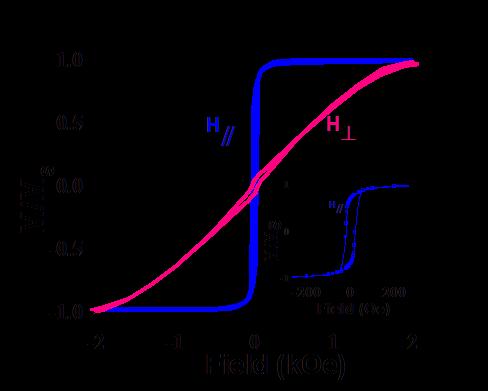
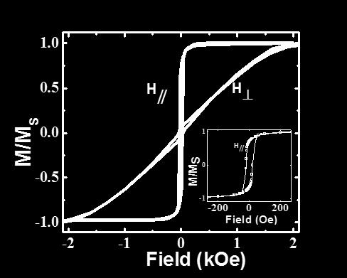
10 In-Plane Uniaxial Anisotropy In-plane rotation 10


 Sachs et al. Sci. Rep.")
11 Device Transfer Technique Graphene exfoliation SiO 2 Si Device fabrication SiO 2 Si Resist spin-coating SiO 2 Si PMMA Device transferred onto target substrate Target substrate PMMA Resist/device layer peel-off PMMA Si DI Water SiO 2 etching SiO 2 Si NaOH solution PMMA Resist lift-off Sachs et al. APL (2014) Sachs et al. Sci. Rep. (2014) Target substrate Gate dielectric: PMMA or h-bn

12 Device Transfer Technique (h-bn Top Gate) 12


13 Device Transfer Technique PMMA Target substrate Transferred devices Si DI Water PMMA/Graphene with contact pads floating in DI water High transfer yield Work for large-area graphene devices Any flat target substrates Sachs et al. Sci. Rep. (2014) Sachs et al. APL (2014)


14 Devices with h-bn Top Gate Before transfer Au/BN/Graphene/SiO 2 After transfer Au/BN/Graphene/YIG YIG Wet transfer h-bn h-bn SiO 2 Top gate Top gate BN-layer is ~30 nm thick. It is much better than PMMA! 14
 Device Characterization Raman Room-temperature Raman spectra of single")
 Both")
15 Intensity (a.u.) Device Characterization Raman Room-temperature Raman spectra of single layer graphene Graphene Graphene on YIG/GGG Before Graphene on SiO 2 /Si YIG/GGG 5μm After Raman Shift (cm -1 ) Both graphene and YIG peaks are identified in the room temperature Raman spectra

 After-transfer:")
 Transfer does not")
16 Before and After Transfer (PMMA Top Gate) Before-transfer: Back-gated through SiO 2 s xx /C s (m 2 /s) Conductivity comparison SiO 2 293K YIG 300K YIG 2K V g (V) After-transfer: Top-gated through PMMA Room temperature mobility slightly increased (6,000 cm 2 /Vs) Transfer does not compromise device quality! 16
 Thin BN top gate BN")


17 Before and After Transfer (BN Top Gate) Thin BN top gate BN SiO 2 No BN SiO 2 Much smaller applied gate voltage (a factor of 15) needed to tune the carrier density over a wide range With h-bn, mobility is enhanced by 6 times, reaching over 30,000 cm 2 /Vs! 17


18 Hall Effecf of Same Graphene on SiO 2, YIG Before transfer SiO 2 Rxy ( ) Overall Hall resistance Linear background H (Oe) After transfer YIG 18

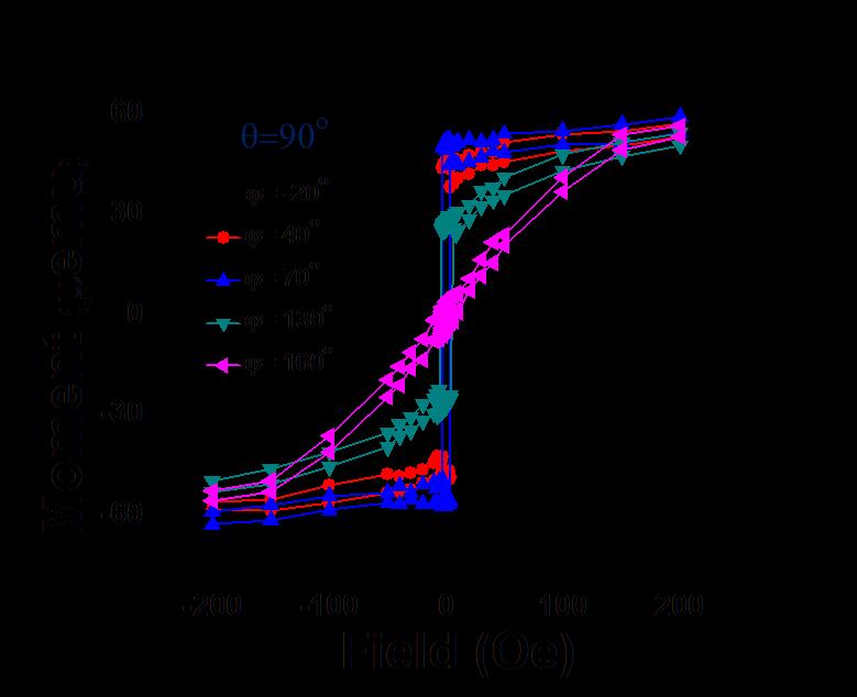
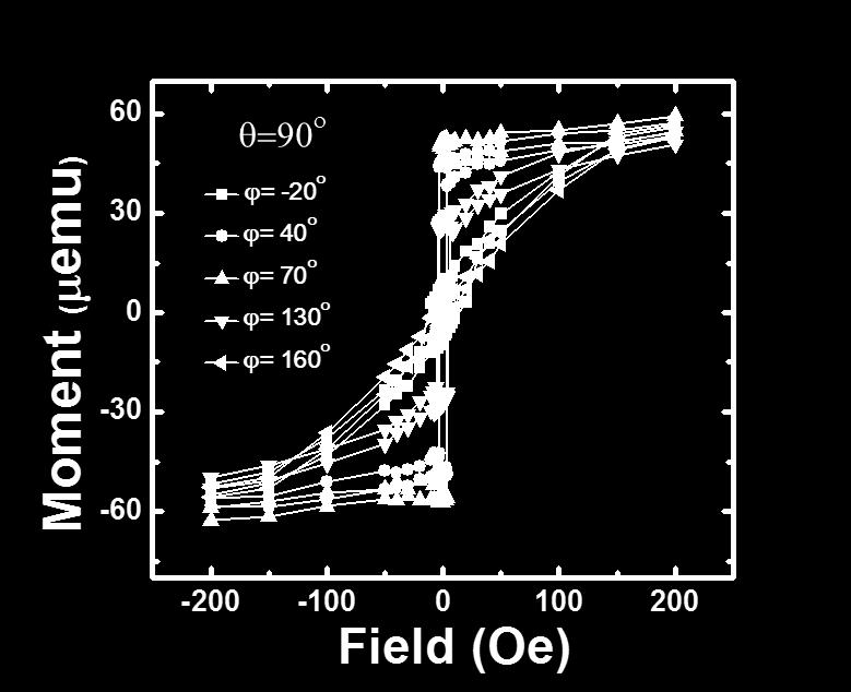
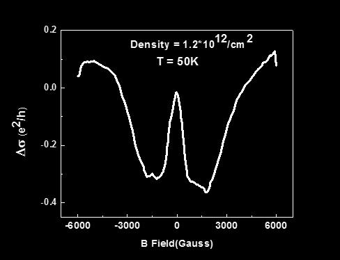
19 Anomalous Hall Effect in Graphene/YIG Ordinary Hall effect R B xy 0 R M s Anomalous Hall effect Hall after linear background removal Magnetization of YIG Х OHE from two carriers Х Stray field effect Ferromagnetic graphene! 19


 AHE")

20 T-Dependence of AHE Temperature dependence 1.0 Magnetization of YIG M/M S B B (G) AHE disappears at ~ 300 K Z.Y.Wang et al. PRL (2015) 20
21 How Strong is Rashba Interaction? Topological band gap ~ smaller of l R and Intrinsic contribution h/t ~ 12 mev: disorder energy scale in our graphene is set to ~ 25 mev Maximum l R is set to 12 mev Observed AHE is likely caused by extrinsic mechanism: skew or side jump 21
22 Towards QAHE in Graphene Need stronger SOC Introduce sp 3 defects Proximity couple graphene to transition metal dichalcogenides Need weaker Disorder Dry transfer 22


23 WS 2 /Graphene Device for direct comparison WS2 Graphene 23


24 Tuning SOC Pristine vs. with WS 2 Conductance Magneto-conductance Suppressed weak-localization in WS 2 covered graphene! Consistent with a SO length of 250 nm 24

25 WS 2 /Graphene WS 2 /Graphene Magneto-conductance Weak anti-localization 25
26 Summary Graphene becomes ferromagnetic when it is exchange coupled to atomically flat YIG ferrimagnetic insulator. AHE is observed SOC already exists at interface. Exchange strength is shown ~26 mev (308 K). 1/5 of quantized anomalous Hall value is obtained. Rashba SOC interaction may be enhanced by introducing sp 3 defects, or by proximity coupling to TMD. All-proximity graphene devices may be needed.


27 Acknowledgement Z.Y. Wang, C. Tang, J.L. Jiang, B.W. Yang, Z.S. Lin, M. Aldosary, R. Sachs, and Y. Barlas B. Cheng and Bockrath group at UCR
An Overview of Spintronics in 2D Materials
 An Overview of Spintronics in 2D Materials Wei Han ( 韩伟 ) 1 2014 ICQM Outline I. Introduction to spintronics (Lecture I) II. Spin injection and detection in 2D (Lecture I) III. Putting magnetic moment
Transport through Andreev Bound States in a Superconductor-Quantum Dot-Graphene System
 Transport through Andreev Bound States in a Superconductor-Quantum Dot-Graphene System Nadya Mason Travis Dirk, Yung-Fu Chen, Cesar Chialvo Taylor Hughes, Siddhartha Lal, Bruno Uchoa Paul Goldbart University
A. Optimizing the growth conditions of large-scale graphene films
 1 A. Optimizing the growth conditions of large-scale graphene films Figure S1. Optical microscope images of graphene films transferred on 300 nm SiO 2 /Si substrates. a, Images of the graphene films grown
Magnetism and Magnetic Materials
 Chapter 2 Magnetism and Magnetic Materials 韩伟 量子材料科学中心 2015 年 9 月 27 日 2014 ICQM 提纲 1. Introduction to magnetism 2. How to induce magnetic moment 3. How to control magnetization 2 Review of last class
Spin-orbit effects in graphene and graphene-like materials. Józef Barnaś
 Spin-orbit effects in graphene and graphene-like materials Józef Barnaś Faculty of Physics, Adam Mickiewicz University, Poznań & Institute of Molecular Physics PAN, Poznań In collaboration with: A. Dyrdał,
Supplementary Information
 Supplementary Information Supplementary Figure 1 AFM and Raman characterization of WS 2 crystals. (a) Optical and AFM images of a representative WS 2 flake. Color scale of the AFM image represents 0-20
Graphene. Tianyu Ye November 30th, 2011
 Graphene Tianyu Ye November 30th, 2011 Outline What is graphene? How to make graphene? (Exfoliation, Epitaxial, CVD) Is it graphene? (Identification methods) Transport properties; Other properties; Applications;
Lecture 20: Semiconductor Structures Kittel Ch 17, p , extra material in the class notes
 Lecture 20: Semiconductor Structures Kittel Ch 17, p 494-503, 507-511 + extra material in the class notes MOS Structure Layer Structure metal Oxide insulator Semiconductor Semiconductor Large-gap Semiconductor
2D MBE Activities in Sheffield. I. Farrer, J. Heffernan Electronic and Electrical Engineering The University of Sheffield
 2D MBE Activities in Sheffield I. Farrer, J. Heffernan Electronic and Electrical Engineering The University of Sheffield Outline Motivation Van der Waals crystals The Transition Metal Di-Chalcogenides
Nanoxide electronics
 Nanoxide electronics Alexey Kalabukhov Quantum Device Physics Laboratory MC2, room D515 Alexei.kalaboukhov@chalmers.se Playing Lego with oxide materials: G. Rijnders, D.H.A. Blank, Nature 433, 369 (2005)
Spin-orbit proximity effects in graphene on TMDCs. Jaroslav Fabian
 Hvar, 4.10.2017 Spin-orbit proximity effects in graphene on TMDCs Jaroslav Fabian Institute for Theoretical Physics University of Regensburg SFB1277 GRK TI SPP 1666 SFB689 GRK1570 SPP 1538 Arbeitsgruppe
Supplementary Figure 1 Magneto-transmission spectra of graphene/h-bn sample 2 and Landau level transition energies of three other samples.
 Supplementary Figure 1 Magneto-transmission spectra of graphene/h-bn sample 2 and Landau level transition energies of three other samples. (a,b) Magneto-transmission ratio spectra T(B)/T(B 0 ) of graphene/h-bn
Fe 1-x Co x Si, a Silicon Based Magnetic Semiconductor
 Fe 1-x Co x Si, a Silicon Based Magnetic Semiconductor T (K) 1 5 Fe.8 Co.2 Si ρ xy (µω cm) J.F. DiTusa N. Manyala LSU Y. Sidis D.P. Young G. Aeppli UCL Z. Fisk FSU T C 1 Nature Materials 3, 255-262 (24)
Nanoxide electronics
 Nanoxide electronics Alexey Kalabukhov Quantum Device Physics Laboratory MC2, room D515 Alexei.kalaboukhov@chalmers.se Playing Lego with oxide materials: G. Rijnders, D.H.A. Blank, Nature 433, 369 (2005)
FIG. 1: (Supplementary Figure 1: Large-field Hall data) (a) AHE (blue) and longitudinal
 (a) AHE (blue) and longitudinal") FIG. 1: (Supplementary Figure 1: Large-field Hall data) (a) AHE (blue) and longitudinal MR (red) of device A at T =2 K and V G - V G 0 = 100 V. Bold blue line is linear fit to large field Hall data (larger
FIG. 1: (Supplementary Figure 1: Large-field Hall data) (a) AHE (blue) and longitudinal MR (red) of device A at T =2 K and V G - V G 0 = 100 V. Bold blue line is linear fit to large field Hall data (larger
What so special about LaAlO3/SrTiO3 interface? Magnetism, Superconductivity and their coexistence at the interface
 What so special about LaAlO3/SrTiO3 interface? Magnetism, Superconductivity and their coexistence at the interface Pramod Verma Indian Institute of Science, Bangalore 560012 July 24, 2014 Pramod Verma
Hidden Interfaces and High-Temperature Magnetism in Intrinsic Topological Insulator - Ferromagnetic Insulator Heterostructures
 Hidden Interfaces and High-Temperature Magnetism in Intrinsic Topological Insulator - Ferromagnetic Insulator Heterostructures Valeria Lauter Quantum Condensed Matter Division, Oak Ridge National Laboratory,
Quantum Hall Effect in Vanishing Magnetic Fields
 Quantum Hall Effect in Vanishing Magnetic Fields Wei Pan Sandia National Labs Sandia is a multi-mission laboratory operated by Sandia Corporation, a Lockheed Martin Company, for the United States Department
SUPPLEMENTARY INFORMATION
 Dirac electron states formed at the heterointerface between a topological insulator and a conventional semiconductor 1. Surface morphology of InP substrate and the device Figure S1(a) shows a 10-μm-square
Self-study problems and questions Processing and Device Technology, FFF110/FYSD13
 Self-study problems and questions Processing and Device Technology, FFF110/FYSD13 Version 2016_01 In addition to the problems discussed at the seminars and at the lectures, you can use this set of problems
Spin Orbit Coupling (SOC) in Graphene
 in Graphene") Spin Orbit Coupling (SOC) in Graphene MMM, Mirko Rehmann, 12.10.2015 Motivation Weak intrinsic SOC in graphene: [84]: Phys. Rev. B 80, 235431 (2009) [85]: Phys. Rev. B 82, 125424 (2010) [86]: Phys. Rev.
Spin Orbit Coupling (SOC) in Graphene MMM, Mirko Rehmann, 12.10.2015 Motivation Weak intrinsic SOC in graphene: [84]: Phys. Rev. B 80, 235431 (2009) [85]: Phys. Rev. B 82, 125424 (2010) [86]: Phys. Rev.
Topological Insulators and Ferromagnets: appearance of flat surface bands
 Topological Insulators and Ferromagnets: appearance of flat surface bands Thomas Dahm University of Bielefeld T. Paananen and T. Dahm, PRB 87, 195447 (2013) T. Paananen et al, New J. Phys. 16, 033019 (2014)
SIGNATURES OF SPIN-ORBIT DRIVEN ELECTRONIC TRANSPORT IN TRANSITION- METAL-OXIDE INTERFACES
 SIGNATURES OF SPIN-ORBIT DRIVEN ELECTRONIC TRANSPORT IN TRANSITION- METAL-OXIDE INTERFACES Nicandro Bovenzi Bad Honnef, 19-22 September 2016 LAO/STO heterostructure: conducting interface between two insulators
Self-Assembly of Two-Dimensional Organic Networks Containing Heavy Metals (Pb, Bi) and Preparation of Spin-Polarized Scanning Tunneling Microscope
 and Preparation of Spin-Polarized Scanning Tunneling Microscope") MPhil Thesis Defense Self-Assembly of Two-Dimensional Organic Networks Containing Heavy Metals (Pb, Bi) and Preparation of Spin-Polarized Scanning Tunneling Microscope Presented by CHEN Cheng 12 th Aug.
MPhil Thesis Defense Self-Assembly of Two-Dimensional Organic Networks Containing Heavy Metals (Pb, Bi) and Preparation of Spin-Polarized Scanning Tunneling Microscope Presented by CHEN Cheng 12 th Aug.
Center for Spintronic Materials, Interfaces, and Novel Architectures. Voltage Controlled Antiferromagnetics and Future Spin Memory
 Center for Spintronic Materials, Interfaces, and Novel Architectures Voltage Controlled Antiferromagnetics and Future Spin Memory Maxim Tsoi The University of Texas at Austin Acknowledgments: H. Seinige,
TRANSVERSE SPIN TRANSPORT IN GRAPHENE
 International Journal of Modern Physics B Vol. 23, Nos. 12 & 13 (2009) 2641 2646 World Scientific Publishing Company TRANSVERSE SPIN TRANSPORT IN GRAPHENE TARIQ M. G. MOHIUDDIN, A. A. ZHUKOV, D. C. ELIAS,
Heusler compounds: Tunable materials with non trivial topologies. Claudia Felser
 Heusler compounds: Tunable materials with non trivial topologies Claudia Felser Tunability of Heusler compounds Tuning the band gap Tuning spin orbit coupling Trivial and topological Heusler Adding spins
Multicolor Graphene Nanoribbon/Semiconductor Nanowire. Heterojunction Light-Emitting Diodes
 Multicolor Graphene Nanoribbon/Semiconductor Nanowire Heterojunction Light-Emitting Diodes Yu Ye, a Lin Gan, b Lun Dai, *a Hu Meng, a Feng Wei, a Yu Dai, a Zujin Shi, b Bin Yu, a Xuefeng Guo, b and Guogang
UNIT - IV SEMICONDUCTORS AND MAGNETIC MATERIALS
 1. What is intrinsic If a semiconductor is sufficiently pure, then it is known as intrinsic semiconductor. ex:: pure Ge, pure Si 2. Mention the expression for intrinsic carrier concentration of intrinsic
Supplementary figures
 Supplementary figures Supplementary Figure 1. A, Schematic of a Au/SRO113/SRO214 junction. A 15-nm thick SRO113 layer was etched along with 30-nm thick SRO214 substrate layer. To isolate the top Au electrodes
with micrometer wide atomic terraces
 Epitaxial growth and properties of La 0.7 Sr 0.3 MnO 3 thin films with micrometer wide atomic terraces Wei Yuan 1, Yuelei Zhao 1, Chi Tang 2, Tang Su 1, Qi Song 1, Jing Shi 2,a), and Wei Han 1,3,b) 1 International
Intrinsic Electronic Transport Properties of High. Information
 Intrinsic Electronic Transport Properties of High Quality and MoS 2 : Supporting Information Britton W. H. Baugher, Hugh O. H. Churchill, Yafang Yang, and Pablo Jarillo-Herrero Department of Physics, Massachusetts
Recent developments in spintronic
 Recent developments in spintronic Tomas Jungwirth nstitute of Physics ASCR, Prague University of Nottingham in collaboration with Hitachi Cambridge, University of Texas, Texas A&M University - Spintronics
Planar Hall Effect in Magnetite (100) Films
 Films") Planar Hall Effect in Magnetite (100) Films Xuesong Jin, Rafael Ramos*, Y. Zhou, C. McEvoy and I.V. Shvets SFI Nanoscience Laboratories, School of Physics, Trinity College Dublin, Dublin 2, Ireland 1 Abstract.
Planar Hall Effect in Magnetite (100) Films Xuesong Jin, Rafael Ramos*, Y. Zhou, C. McEvoy and I.V. Shvets SFI Nanoscience Laboratories, School of Physics, Trinity College Dublin, Dublin 2, Ireland 1 Abstract.
Physics of Semiconductors
 Physics of Semiconductors 13 th 2016.7.11 Shingo Katsumoto Department of Physics and Institute for Solid State Physics University of Tokyo Outline today Laughlin s justification Spintronics Two current
Supporting Information for: Gate-Variable Mid-Infrared Optical Transitions in a (Bi 1-
 Supporting Information for: Gate-Variable Mid-Infrared Optical Transitions in a (Bi 1- xsb x ) 2 Te 3 Topological Insulator 1 William S. Whitney, 2,3 Victor W. Brar, 4 Yunbo Ou, 5,6 Yinming Shao, 2 Artur
Spatiotemporal magnetic imaging at the nanometer and picosecond scales
 AFOSR Nanoelectronics Review, Oct. 24, 2016 Spatiotemporal magnetic imaging at the nanometer and picosecond scales Gregory D. Fuchs School of Applied & Engineering Physics, Cornell University T M V TRANE
Chun Ning Lau (Jeanie) Quantum Transport! in! 2D Atomic Membranes!
 Quantum Transport! in! 2D Atomic Membranes!") Chun Ning Lau (Jeanie) Quantum Transport! in! 2D Atomic Membranes! 2D Materials and Heterostructures! hbn MoS 2 WSe 2 Fluorographene Geim, Nature 2013. Conductors, e.g. graphene, few-layer graphene Semiconductors,
Chun Ning Lau (Jeanie) Quantum Transport! in! 2D Atomic Membranes! 2D Materials and Heterostructures! hbn MoS 2 WSe 2 Fluorographene Geim, Nature 2013. Conductors, e.g. graphene, few-layer graphene Semiconductors,
Impact of disorder and topology in two dimensional systems at low carrier densities
 Impact of disorder and topology in two dimensional systems at low carrier densities A Thesis Submitted For the Degree of Doctor of Philosophy in the Faculty of Science by Mohammed Ali Aamir Department
0.002 ( ) R xy
 R xy") a b z 0.002 x H y R xy () 0.000-0.002 0 90 180 270 360 (degree) Supplementary Figure 1. Planar Hall effect resistance as a function of the angle of an in-plane field. a, Schematic of the planar Hall resistance
a b z 0.002 x H y R xy () 0.000-0.002 0 90 180 270 360 (degree) Supplementary Figure 1. Planar Hall effect resistance as a function of the angle of an in-plane field. a, Schematic of the planar Hall resistance
Ferromagnetic resonance in Yttrium Iron Garnet
 Author:. Facultat de Física, Universitat de Barcelona, Diagonal 645, 08028 Barcelona, Spain. Advisor: Joan Manel Hernàndez Ferràs Abstract: his work presents a study of the ferromagnetic resonance of an
InAs/GaSb A New 2D Topological Insulator
 InAs/GaSb A New 2D Topological Insulator 1. Old Material for New Physics 2. Quantized Edge Modes 3. Adreev Reflection 4. Summary Rui-Rui Du Rice University Superconductor Hybrids Villard de Lans, France
TOPOLOGICAL BANDS IN GRAPHENE SUPERLATTICES
 TOPOLOGICAL BANDS IN GRAPHENE SUPERLATTICES 1) Berry curvature in superlattice bands 2) Energy scales for Moire superlattices 3) Spin-Hall effect in graphene Leonid Levitov (MIT) @ ISSP U Tokyo MIT Manchester
Graphene Fundamentals and Emergent Applications
 Graphene Fundamentals and Emergent Applications Jamie H. Warner Department of Materials University of Oxford Oxford, UK Franziska Schaffel Department of Materials University of Oxford Oxford, UK Alicja
Challenges and Opportunities. Prof. J. Raynien Kwo 年
 Nanoelectronics Beyond Si: Challenges and Opportunities Prof. J. Raynien Kwo 年 立 Si CMOS Device Scaling Beyond 22 nm node High κ,, Metal gates, and High mobility channel 1947 First Transistor 1960 1960
Spin injection. concept and technology
 Spin injection concept and technology Ron Jansen ャンセンロン Spintronics Research Center National Institute of Advanced Industrial Science and Technology (AIST), Tsukuba, Japan Spin injection Transfer of spin
Challenges for Materials to Support Emerging Research Devices
 Challenges for Materials to Support Emerging Research Devices C. Michael Garner*, James Hutchby +, George Bourianoff*, and Victor Zhirnov + *Intel Corporation Santa Clara, CA + Semiconductor Research Corporation
Mesoscopic Spintronics
 Mesoscopic Spintronics Taro WAKAMURA (Université Paris-Sud) Lecture 2 Today s Topics 2.1 Anomalous Hall effect and spin Hall effect 2.2 Spin Hall effect measurements 2.3 Interface effects Anomalous Hall
Making Semiconductors Ferromagnetic: Opportunities and Challenges
 Making Semiconductors Ferromagnetic: Opportunities and Challenges J.K. Furdyna University of Notre Dame Collaborators: X. Liu and M. Dobrowolska, University of Notre Dame T. Wojtowicz, Institute of Physics,
From nanophysics research labs to cell phones. Dr. András Halbritter Department of Physics associate professor
 From nanophysics research labs to cell phones Dr. András Halbritter Department of Physics associate professor Curriculum Vitae Birth: 1976. High-school graduation: 1994. Master degree: 1999. PhD: 2003.
STM and graphene. W. W. Larry Pai ( 白偉武 ) Center for condensed matter sciences, National Taiwan University NTHU, 2013/05/23
 Center for condensed matter sciences, National Taiwan University NTHU, 2013/05/23") STM and graphene W. W. Larry Pai ( 白偉武 ) Center for condensed matter sciences, National Taiwan University NTHU, 2013/05/23 Why graphene is important: It is a new form of material (two dimensional, single
STM and graphene W. W. Larry Pai ( 白偉武 ) Center for condensed matter sciences, National Taiwan University NTHU, 2013/05/23 Why graphene is important: It is a new form of material (two dimensional, single
SUPPLEMENTARY INFORMATION
 doi:.38/nature09979 I. Graphene material growth and transistor fabrication Top-gated graphene RF transistors were fabricated based on chemical vapor deposition (CVD) grown graphene on copper (Cu). Cu foil
Electronics with 2D Crystals: Scaling extender, or harbinger of new functions?
 Electronics with 2D Crystals: Scaling extender, or harbinger of new functions? 1 st Workshop on Data Abundant Systems Technology Stanford, April 2014 Debdeep Jena (djena@nd.edu) Electrical Engineering,
Enhanced spin orbit torques by oxygen incorporation in tungsten films
 Enhanced spin orbit torques by oxygen incorporation in tungsten films Timothy Phung IBM Almaden Research Center, San Jose, California, USA 1 Motivation: Memory devices based on spin currents Spin Transfer
Outline. Introduction: graphene. Adsorption on graphene: - Chemisorption - Physisorption. Summary
 Outline Introduction: graphene Adsorption on graphene: - Chemisorption - Physisorption Summary 1 Electronic band structure: Electronic properties K Γ M v F = 10 6 ms -1 = c/300 massless Dirac particles!
Supporting Information
 Electronic Supplementary Material (ESI) for ChemComm. This journal is The Royal Society of Chemistry 2014 Supporting Information Controllable Atmospheric Pressure Growth of Mono-layer, Bi-layer and Tri-layer
Tuning Rashba Spin-Orbit Coupling in Gated Multi-layer InSe
 Supporting Information Tuning Rashba Spin-Orbit Coupling in Gated Multi-layer InSe Kasun Premasiri, Santosh Kumar Radha, Sukrit Sucharitakul, U. Rajesh Kumar, Raman Sankar,, Fang-Cheng Chou, Yit-Tsong
Lecture 20 - Semiconductor Structures
 Lecture 0: Structures Kittel Ch 17, p 494-503, 507-511 + extra material in the class notes MOS Structure metal Layer Structure Physics 460 F 006 Lect 0 1 Outline What is a semiconductor Structure? Created
Spin Current and Spin Seebeck Effect
 at Rome, Italy (September 18, 2013) Spin Current and Spin Seebeck Effect Sadamichi Maekawa Advanced Science Research Center (ASRC), Japan Atomic Energy Agency (JAEA) at Tokai and CREST-JST. Co-workers:
Physics in Quasi-2D Materials for Spintronics Applications
 Physics in Quasi-2D Materials for Spintronics Applications Topological Insulators and Graphene Ching-Tzu Chen IBM TJ Watson Research Center May 13, 2016 2016 C-SPIN Topological Spintronics Device Workshop
Spin-orbit Effects in Semiconductor Spintronics. Laurens Molenkamp Physikalisches Institut (EP3) University of Würzburg
 University of Würzburg") Spin-orbit Effects in Semiconductor Spintronics Laurens Molenkamp Physikalisches Institut (EP3) University of Würzburg Collaborators Hartmut Buhmann, Charlie Becker, Volker Daumer, Yongshen Gui Matthias
Spin-orbit Effects in Semiconductor Spintronics Laurens Molenkamp Physikalisches Institut (EP3) University of Würzburg Collaborators Hartmut Buhmann, Charlie Becker, Volker Daumer, Yongshen Gui Matthias
SUPPLEMENTARY INFORMATION. Observation of tunable electrical bandgap in large-area twisted bilayer graphene synthesized by chemical vapor deposition
 SUPPLEMENTARY INFORMATION Observation of tunable electrical bandgap in large-area twisted bilayer graphene synthesized by chemical vapor deposition Jing-Bo Liu 1 *, Ping-Jian Li 1 *, Yuan-Fu Chen 1, Ze-Gao
GRAPHENE ON THE Si-FACE OF SILICON CARBIDE USER MANUAL
 GRAPHENE ON THE Si-FACE OF SILICON CARBIDE USER MANUAL 1. INTRODUCTION Silicon Carbide (SiC) is a wide band gap semiconductor that exists in different polytypes. The substrate used for the fabrication
Supporting Online Material for
 www.sciencemag.org/cgi/content/full/327/5966/662/dc Supporting Online Material for 00-GHz Transistors from Wafer-Scale Epitaxial Graphene Y.-M. Lin,* C. Dimitrakopoulos, K. A. Jenkins, D. B. Farmer, H.-Y.
SUPPLEMENTARY INFORMATION
 SUPPLEMENTARY INFORMATION Facile Synthesis of High Quality Graphene Nanoribbons Liying Jiao, Xinran Wang, Georgi Diankov, Hailiang Wang & Hongjie Dai* Supplementary Information 1. Photograph of graphene
Broken Symmetry States and Divergent Resistance in Suspended Bilayer Graphene
 Broken Symmetry States and Divergent Resistance in Suspended Bilayer Graphene The Harvard community has made this article openly available. Please share how this access benefits you. Your story matters.
Graphene The Search For Two Dimensions. Christopher Scott Friedline Arizona State University
 Graphene The Search For Two Dimensions Christopher Scott Friedline Arizona State University What Is Graphene? Single atomic layer of graphite arranged in a honeycomb crystal lattice Consists of sp 2 -bonded
Observation of the intrinsic inverse spin Hall effect from ferromagnet
 Observation of the intrinsic inverse spin Hall effect from ferromagnet Ayaka Tsukahara #, Yuta Kitamura #, Eiji Shikoh, Yuichiro Ando, Teruya Shinjo and Masashi Shiraishi * # Graduate School of Engineering
Edge conduction in monolayer WTe 2
 In the format provided by the authors and unedited. DOI: 1.138/NPHYS491 Edge conduction in monolayer WTe 2 Contents SI-1. Characterizations of monolayer WTe2 devices SI-2. Magnetoresistance and temperature
Classification of Solids
 Classification of Solids Classification by conductivity, which is related to the band structure: (Filled bands are shown dark; D(E) = Density of states) Class Electron Density Density of States D(E) Examples
Cover Page. The handle holds various files of this Leiden University dissertation
 Cover Page The handle http://hdl.handle.net/1887/24306 holds various files of this Leiden University dissertation Author: Verhagen, T.G.A. Title: Magnetism and magnetization dynamics in thin film ferromagnets
Experimental observation of the quantum anomalous Hall effect in a magnetic topological insulator
 Experimental observation of the quantum anomalous Hall effect in a magnetic topological insulator Cui-Zu Chang, 1,2 Jinsong Zhang, 1 Xiao Feng, 1,2 Jie Shen, 2 Zuocheng Zhang, 1 Minghua Guo, 1 Kang Li,
Observation of the intrinsic inverse spin Hall effect in Ni 80 Fe 20. Yuichiro Ando, Teruya Shinjo and Masashi Shiraishi * #
 Observation of the intrinsic inverse spin Hall effect in Ni 80 Fe 20 Ayaka Tsukahara #, Yuta Kitamura #, Eiji Shikoh, Yuichiro Ando, Teruya Shinjo and Masashi Shiraishi * # Graduate School of Engineering
b) Discuss the amplitude of electromagnetic waves on reflection and refraction at the boundary of a dielectric interface.
 Discuss the amplitude of electromagnetic waves on reflection and refraction at the boundary of a dielectric interface.") (DPHY 21) ASSIGNMENT - 1, DEC - 2018. PAPER- V : ELECTROMAGNETIC THEORY AND MODERN OPTICS 1) a)derive Fresnel equation. b) Discuss the amplitude of electromagnetic waves on reflection and refraction at
(DPHY 21) ASSIGNMENT - 1, DEC - 2018. PAPER- V : ELECTROMAGNETIC THEORY AND MODERN OPTICS 1) a)derive Fresnel equation. b) Discuss the amplitude of electromagnetic waves on reflection and refraction at
Correlated 2D Electron Aspects of the Quantum Hall Effect
 Correlated 2D Electron Aspects of the Quantum Hall Effect Magnetic field spectrum of the correlated 2D electron system: Electron interactions lead to a range of manifestations 10? = 4? = 2 Resistance (arb.
SOLID STATE PHYSICS. Second Edition. John Wiley & Sons. J. R. Hook H. E. Hall. Department of Physics, University of Manchester
 SOLID STATE PHYSICS Second Edition J. R. Hook H. E. Hall Department of Physics, University of Manchester John Wiley & Sons CHICHESTER NEW YORK BRISBANE TORONTO SINGAPORE Contents Flow diagram Inside front
Coulomb Drag in Graphene
 Graphene 2017 Coulomb Drag in Graphene -Toward Exciton Condensation Philip Kim Department of Physics, Harvard University Coulomb Drag Drag Resistance: R D = V 2 / I 1 Onsager Reciprocity V 2 (B)/ I 1 =
High-precision observation of nonvolatile quantum anomalous Hall effect
 High-precision observation of nonvolatile quantum anomalous Hall effect The MIT Faculty has made this article openly available. Please share how this access benefits you. Your story matters. Citation As
(DPHY 21) 1) a) Discuss the propagation of light in conducting surface. b) Discuss about the metallic reflection at oblique incidence.
 1) a) Discuss the propagation of light in conducting surface. b) Discuss about the metallic reflection at oblique incidence.") (DPHY 21) ASSIGNMENT - 1, MAY - 2015. PAPER- V : ELECTROMAGNETIC THEORY AND MODERN OPTICS 1) a) Discuss the propagation of light in conducting surface. b) Discuss about the metallic reflection at oblique
(DPHY 21) ASSIGNMENT - 1, MAY - 2015. PAPER- V : ELECTROMAGNETIC THEORY AND MODERN OPTICS 1) a) Discuss the propagation of light in conducting surface. b) Discuss about the metallic reflection at oblique
Quantum anomalous Hall states on decorated magnetic surfaces
 Quantum anomalous Hall states on decorated magnetic surfaces David Vanderbilt Rutgers University Kevin Garrity & D.V. Phys. Rev. Lett.110, 116802 (2013) Recently: Topological insulators (TR-invariant)
Bloch, Landau, and Dirac: Hofstadter s Butterfly in Graphene. Philip Kim. Physics Department, Columbia University
 Bloch, Landau, and Dirac: Hofstadter s Butterfly in Graphene Philip Kim Physics Department, Columbia University Acknowledgment Prof. Cory Dean (now at CUNY) Lei Wang Patrick Maher Fereshte Ghahari Carlos
1. Nanotechnology & nanomaterials -- Functional nanomaterials enabled by nanotechnologies.
 Novel Nano-Engineered Semiconductors for Possible Photon Sources and Detectors NAI-CHANG YEH Department of Physics, California Institute of Technology 1. Nanotechnology & nanomaterials -- Functional nanomaterials
Spin orbit torque driven magnetic switching and memory. Debanjan Bhowmik
 Spin orbit torque driven magnetic switching and memory Debanjan Bhowmik Spin Transfer Torque Fixed Layer Free Layer Fixed Layer Free Layer Current coming out of the fixed layer (F2) is spin polarized in
Physics in two dimensions in the lab
 Physics in two dimensions in the lab Nanodevice Physics Lab David Cobden PAB 308 Collaborators at UW Oscar Vilches (Low Temperature Lab) Xiaodong Xu (Nanoscale Optoelectronics Lab) Jiun Haw Chu (Quantum
Magnetic tunnel junctions using Co-based Heusler alloy electrodes
 Magnetic tunnel junctions using Co-based Heusler alloy electrodes 1 Half-metallic Heusler alloy thin films for spintronic devices E F E Energy gap Co 2 YZ: L2 1 structure 2a MgO.5957 nm a Co.5654 2MnSi
Lecture 150 Basic IC Processes (10/10/01) Page ECE Analog Integrated Circuits and Systems P.E. Allen
 Page ECE Analog Integrated Circuits and Systems P.E. Allen") Lecture 150 Basic IC Processes (10/10/01) Page 1501 LECTURE 150 BASIC IC PROCESSES (READING: TextSec. 2.2) INTRODUCTION Objective The objective of this presentation is: 1.) Introduce the fabrication of
Lecture 150 Basic IC Processes (10/10/01) Page 1501 LECTURE 150 BASIC IC PROCESSES (READING: TextSec. 2.2) INTRODUCTION Objective The objective of this presentation is: 1.) Introduce the fabrication of
2D Materials for Gas Sensing
 2D Materials for Gas Sensing S. Guo, A. Rani, and M.E. Zaghloul Department of Electrical and Computer Engineering The George Washington University, Washington DC 20052 Outline Background Structures of
InAs/GaSb A New Quantum Spin Hall Insulator
 InAs/GaSb A New Quantum Spin Hall Insulator Rui-Rui Du Rice University 1. Old Material for New Physics 2. Quantized Edge Modes 3. Andreev Reflection 4. Summary KITP Workshop on Topological Insulator/Superconductor
Chun Ning Lau (Jeanie) Graphene Quantum Electronics: p-n Junctions and Atomic Switches
 Graphene Quantum Electronics: p-n Junctions and Atomic Switches") Chun Ning Lau (Jeanie) Graphene Quantum Electronics: p-n Junctions and Atomic Switches Acknowledgement Graduate Students Feng Miao Wenzhong Bao Discussion With Shan-Wan Tsai, Antonio Castro-Neto, Michael
Chun Ning Lau (Jeanie) Graphene Quantum Electronics: p-n Junctions and Atomic Switches Acknowledgement Graduate Students Feng Miao Wenzhong Bao Discussion With Shan-Wan Tsai, Antonio Castro-Neto, Michael
Topologically Insulating Properties of Doping-free Bi 2 Se 3 Single Crystals
 Topologically Insulating Properties of Doping-free Bi 2 Se 3 Single Crystals POSTECH-APCTP AMS Workshop September 6, 2010; Pohang Hu-Jong Lee Pohang University of Science and Technology (POSTECH) Quantum
Spin caloritronics in magnetic/non-magnetic nanostructures and graphene field effect devices Dejene, Fasil
 University of Groningen Spin caloritronics in magnetic/non-magnetic nanostructures and graphene field effect devices Dejene, Fasil DOI: 10.1038/nphys2743 IMPORTANT NOTE: You are advised to consult the
A BIT OF MATERIALS SCIENCE THEN PHYSICS
 GRAPHENE AND OTHER D ATOMIC CRYSTALS Andre Geim with many thanks to K. Novoselov, S. Morozov, D. Jiang, F. Schedin, I. Grigorieva, J. Meyer, M. Katsnelson A BIT OF MATERIALS SCIENCE THEN PHYSICS CARBON
The Quantum Spin Hall Effect
 The Quantum Spin Hall Effect Shou-Cheng Zhang Stanford University with Andrei Bernevig, Taylor Hughes Science, 314,1757 2006 Molenamp et al, Science, 318, 766 2007 XL Qi, T. Hughes, SCZ preprint The quantum
Stripes developed at the strong limit of nematicity in FeSe film
 Stripes developed at the strong limit of nematicity in FeSe film Wei Li ( ) Department of Physics, Tsinghua University IASTU Seminar, Sep. 19, 2017 Acknowledgements Tsinghua University Prof. Qi-Kun Xue,
All-electrical measurements of direct spin Hall effect in GaAs with Esaki diode electrodes.
 All-electrical measurements of direct spin Hall effect in GaAs with Esaki diode electrodes. M. Ehlert 1, C. Song 1,2, M. Ciorga 1,*, M. Utz 1, D. Schuh 1, D. Bougeard 1, and D. Weiss 1 1 Institute of Experimental
Chern insulator and Chern half-metal states in the two-dimensional. spin-gapless semiconductor Mn 2 C 6 S 12
 Supporting Information for Chern insulator and Chern half-metal states in the two-dimensional spin-gapless semiconductor Mn 2 C 6 S 12 Aizhu Wang 1,2, Xiaoming Zhang 1, Yuanping Feng 3 * and Mingwen Zhao
NiCl2 Solution concentration. Etching Duration. Aspect ratio. Experiment Atmosphere Temperature. Length(µm) Width (nm) Ar:H2=9:1, 150Pa
 Width (nm) Ar:H2=9:1, 150Pa") Experiment Atmosphere Temperature #1 # 2 # 3 # 4 # 5 # 6 # 7 # 8 # 9 # 10 Ar:H2=9:1, 150Pa Ar:H2=9:1, 150Pa Ar:H2=9:1, 150Pa Ar:H2=9:1, 150Pa Ar:H2=9:1, 150Pa Ar:H2=9:1, 150Pa Ar:H2=9:1, 150Pa Ar:H2=9:1,
Experiment Atmosphere Temperature #1 # 2 # 3 # 4 # 5 # 6 # 7 # 8 # 9 # 10 Ar:H2=9:1, 150Pa Ar:H2=9:1, 150Pa Ar:H2=9:1, 150Pa Ar:H2=9:1, 150Pa Ar:H2=9:1, 150Pa Ar:H2=9:1, 150Pa Ar:H2=9:1, 150Pa Ar:H2=9:1,
Spin pumping and spin transport in magne0c metal and insulator heterostructures. Eric Montoya Surface Science Laboratory Simon Fraser University
 Spin pumping and spin transport in magne0c metal and insulator heterostructures Eric Montoya Surface Science Laboratory Simon Fraser University Why use spin currents? We can eliminate circumvent these
Carbon based Nanoscale Electronics
 Carbon based Nanoscale Electronics 09 02 200802 2008 ME class Outline driving force for the carbon nanomaterial electronic properties of fullerene exploration of electronic carbon nanotube gold rush of
High Temperature Ferromagnetism in GaAs-based Heterostructures. with Mn Delta Doping
 High Temperature Ferromagnetism in GaAs-based Heterostructures with Mn Delta Doping A. M. Nazmul, 1,2 T. Amemiya, 1 Y. Shuto, 1 S. Sugahara, 1 and M. Tanaka 1,2 1. Department of Electronic Engineering,