Introduction to Nanotechnology Chapter 5 Carbon Nanostructures Lecture 1
|
|
|
- Charlotte Helena Pierce
- 6 years ago
- Views:
Transcription
1 Introduction to Nanotechnology Chapter 5 Carbon Nanostructures Lecture 1 ChiiDong Chen Institute of Physics, Academia Sinica chiidong@phys.sinica.edu.tw

2 Carbon contains 6 electrons: (1s) 2, (2s), (2p x ), (2p y ), (2p z ) p x, p y, p z orbitals of carbon atom sp 3 hybridization in CH 4 Ψ = s + λ p + λ p + λ p x x y y z z Diamond : tetrahedral bond through sp 3 hybrid bonds Graphite sheet: hexagon bond through sp 2 hybrid bonds

3 Fig. 4.2 Apparatus for laser evaporation of nanoparticles Fig. 5.3 Mass spectrum of Carbon clusters. The C 60 and C 70 peaks are evident.
4 Fig. 5.4 Result of molecular orbital theory for the structure of small clusters Odd N: linear structure, sp hybridization Even N: closed structure
 is due to absorption from C 60 presented in interstellar dust.")
5 Optical extinction Carbon Star (Red giant) C 60 molecules are created in the outer atmosphere of a red giant Optical spectrum of light coming from stars in outer space. The peak at 5.6eV (220nm) is due to absorption from C 60 presented in interstellar dust.

 surfaces, and hexagons lead to")
6 1.388 Å (C=C:1.34 Å) 1.432Å (C-C:1.53 Å) 7.1 Å Fig. 5.6 structure of C 60 fullerene molecule Atoms are held together by van der Waals forces contains 12 pentagonal and 20 hexagonal The pentagons are needed to produce closed ( convex ) surfaces, and hexagons lead to a planar surface.
7 Dissolves in common solvents like benzene, toluene, hexane Readily vaporizes in vacuum around 400 C Low thermal conductivity Pure C 60 is an electrical insulator C 60 doped with alkali metals shows a range of electrical conductivity: Insulator (K 6 C 60 ) to superconductor (K 3 C 60 ) < 30 K! 6 neighbors K + C with 3 ionized K + Highly disordered material C 60 Other superconducting compounds: Rb 3 C 60, Cs 3 C 60, Na 3 C 60 4 neighbors
8 Superconductivity in K 3 C 60 K 3 C 60 :18K Cs 2 RbC 60 : 33K A 3 C 60, A=Alkali K 3 C 60

] C")
9 Various sizes of fullerenes The Smallest Fullerene C 20 Gas-phase production and photoelectron spectroscopy of the smallest fullerene, C 20 [Nature, 407, 60 (2000)] C 70

10 Break junction approach for electrical measurement of a single nano-particle IV at 1.5K 5nm CdSe Fabrication of metallic electrodes with nanometer separation by electromigration [APL, 75, 301 (1999)] 7nm CdSe
11 IV characteristics of a single C 60 transistor at 1.5K Nature 407, 58 (2000) Figure 1 Current voltage ( I V) curves obtained from a single-c 60 transistor at T= 1.5 K. Five I V curves taken at different gate voltages ( Vg) are shown. Single-C 60 transistors were prepared by first depositing a dilute toluene solution of C60 onto a pair of connected gold electrodes. A gap of,1 nm was then created using electromigrationinduced breaking of the electrodes. Upper inset, a large bias was applied between the electrodes while the current through the connected electrode was monitored (black solid curve). After the initial rapid decrease (solid arrow), the conductance stayed above,0.05 ms up to,2.0 V. This behaviour was observed in most single-c 60 transistors, but it was not observed when no C 60 solution was deposited (red dotted curve). The bias voltage was increased until the conductance fell low enough to ensure that the current through the junction was in the tunnelling regime (open arrow). The low bias measurements shown in the main panel were taken after the breaking procedure. Lower inset, an idealized diagram of a single C60-transistor formed by this method.

 through pink to white (white representing 30 ns in a, b and c and 5 ns in d).")
12 In large bias range Charging energy > 270meV Two-dimensional differential conductance ( I/ V) plots as a function of the bias voltage (V) and the gate voltage (V g ). Data were obtained from four different devices prepared from separate fabrication runs. The dark triangular regions correspond to the conductance gap, and the bright lines represent peaks in the differential conductance. a d, The differential conductance values are represented by the colour scale, which changes from black (0 ns) through pink to white (white representing 30 ns in a, b and c and 5 ns in d). The white arrows mark the point where I/ V lines intercept the conductance gap. During the acquisition of data in d, one switch where the entire I/ V characteristics shift along the V g axis occurred at V g = 1.15 V. The right portion of the plot d is shifted along the V g axis to preserve the continuity of the lines.

13 6.2Å K 70N/m f 1.2THz hf 5meV δ 4pm Figure 4 Diagram of the centre-of-mass oscillation of C 60. a, A C 60 molecule is bound to the gold surface by the van der Waals and electrostatic interaction. The interaction potential is shown schematically alongside. The potential near the equilibrium position can be approximated well by a harmonic potential with a force constant k. This harmonic potential gives quantized energy levels with frequency f= 1/2π(k/ M) 1/2. Here M represents the mass of C 60 and his the Planck constant. b, When an electron jumps on to C n- 60, the attractive interaction between the additional electron and its image charge on gold pulls the C60 ion closer to the gold surface by the distance d. This electrostatic interaction results in the mechanical motion of C60.
14 Laser evaporation Chemical vapor deposition: method: methane (CH 4 ) 1100ºC Catalyst Co or Ni


15 Fabrication of the nanotube devices Fe catalyst + multiwalled carbon nanotubes grown by CVD Fe Si+SiO 2 chip 1µm Cr leads 10 µm Au leads made by photo-lithography Cr electrodes made by e-beam lithography

16 Growth Conditions: Substrate: 300nm thermally grown SiO 2 Catalyst: 9-nm-thermally evaporated iron pads Pretreatment: 1mBar hydrogen, ~700 C, 5 min Growth: 1mBar ethylene, ~750 C, 5 min
17 22.5 nm 18 layers 20 nm 10 nm TEM
18 Multiwall nanotube consists of capped concentric cylinders separated by ~ 3.5 Å. Typically, outer diameter of carbon nanotubes prepared by a carbon arc process ranges between 20 and 200 Å, and inner diameter ranges between 10 and 30 Å. Typical lengths of the arc-grown tubules are about 1 m, giving rise to an aspect ratio (length-to-diameter ratio) of 10 2 to 10 3.

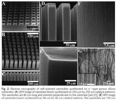
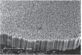
19 Forests of multiwalled carbon nanotubes
20
Introduction to Nanotechnology Chapter 5 Carbon Nanostructures Lecture 1
 Introduction to Nanotechnology Chapter 5 Carbon Nanostructures Lecture 1 ChiiDong Chen Institute of Physics, Academia Sinica chiidong@phys.sinica.edu.tw 02 27896766 Section 5.2.1 Nature of the Carbon Bond
Single Electron Tunneling Examples
 Single Electron Tunneling Examples Danny Porath 2002 (Schönenberger et. al.) It has long been an axiom of mine that the little things are infinitely the most important Sir Arthur Conan Doyle Books and
Transport through Andreev Bound States in a Superconductor-Quantum Dot-Graphene System
 Transport through Andreev Bound States in a Superconductor-Quantum Dot-Graphene System Nadya Mason Travis Dirk, Yung-Fu Chen, Cesar Chialvo Taylor Hughes, Siddhartha Lal, Bruno Uchoa Paul Goldbart University
Unit 2: Structure and Bonding
 Elements vs Compounds Elements are substances made of one kind of atom. There are around 100 elements, which are listed in the Periodic Table. Elements may chemically combine (bond) together in fixed proportions
DocumentToPDF trial version, to remove this mark, please register this software.
 PAPER PRESENTATION ON Carbon Nanotube - Based Nonvolatile Random Access Memory AUTHORS M SIVARAM PRASAD Sivaram.443@gmail.com B N V PAVAN KUMAR pavankumar.bnv@gmail.com 1 Carbon Nanotube- Based Nonvolatile
Carbon nanomaterials. Gavin Lawes Wayne State University.
 Carbon nanomaterials Gavin Lawes Wayne State University glawes@wayne.edu Outline 1. Carbon structures 2. Carbon nanostructures 3. Potential applications for Carbon nanostructures Periodic table from bpc.edu
Fabrication Technology, Part I
 EEL5225: Principles of MEMS Transducers (Fall 2004) Fabrication Technology, Part I Agenda: Microfabrication Overview Basic semiconductor devices Materials Key processes Oxidation Thin-film Deposition Reading:
Seminars in Nanosystems - I
 Seminars in Nanosystems - I Winter Semester 2011/2012 Dr. Emanuela Margapoti Emanuela.Margapoti@wsi.tum.de Dr. Gregor Koblmüller Gregor.Koblmueller@wsi.tum.de Seminar Room at ZNN 1 floor Topics of the
Electric Field-Dependent Charge-Carrier Velocity in Semiconducting Carbon. Nanotubes. Yung-Fu Chen and M. S. Fuhrer
 Electric Field-Dependent Charge-Carrier Velocity in Semiconducting Carbon Nanotubes Yung-Fu Chen and M. S. Fuhrer Department of Physics and Center for Superconductivity Research, University of Maryland,
The many forms of carbon
 The many forms of carbon Carbon is not only the basis of life, it also provides an enormous variety of structures for nanotechnology. This versatility is connected to the ability of carbon to form two
Supporting Information
 Supporting Information Molecular Orbital Gating Surface-Enhanced Raman Scattering Chenyang Guo, 1, Xing Chen, 2, Song-Yuan Ding, 3, Dirk Mayer, 4 Qingling Wang, 1 Zhikai Zhao, 1,5 Lifa Ni, 1,6 Haitao Liu,
Nanoelectronics. Topics
 Nanoelectronics Topics Moore s Law Inorganic nanoelectronic devices Resonant tunneling Quantum dots Single electron transistors Motivation for molecular electronics The review article Overview of Nanoelectronic
4.2.1 Chemical bonds, ionic, covalent and metallic
 4.2 Bonding, structure, and the properties of matter Chemists use theories of structure and bonding to explain the physical and chemical properties of materials. Analysis of structures shows that atoms
Chemical bonds. In some minerals, other (less important) bond types include:
 bond types include:") Chemical bonds Chemical bond: force of attraction between two or more atoms/ions Types of bonds in crystals: Ionic bond: electrostatic attraction between two oppositely charged ions. This type of bond
Chemical bonds Chemical bond: force of attraction between two or more atoms/ions Types of bonds in crystals: Ionic bond: electrostatic attraction between two oppositely charged ions. This type of bond
Nanostructure. Materials Growth Characterization Fabrication. More see Waser, chapter 2
 Nanostructure Materials Growth Characterization Fabrication More see Waser, chapter 2 Materials growth - deposition deposition gas solid Physical Vapor Deposition Chemical Vapor Deposition Physical Vapor
Supplementary Figure S1. AFM images of GraNRs grown with standard growth process. Each of these pictures show GraNRs prepared independently,
 Supplementary Figure S1. AFM images of GraNRs grown with standard growth process. Each of these pictures show GraNRs prepared independently, suggesting that the results is reproducible. Supplementary Figure
Supporting Information
 Supporting Information Assembly and Densification of Nanowire Arrays via Shrinkage Jaehoon Bang, Jonghyun Choi, Fan Xia, Sun Sang Kwon, Ali Ashraf, Won Il Park, and SungWoo Nam*,, Department of Mechanical
single-electron electron tunneling (SET)
") single-electron electron tunneling (SET) classical dots (SET islands): level spacing is NOT important; only the charging energy (=classical effect, many electrons on the island) quantum dots: : level spacing
single-electron electron tunneling (SET) classical dots (SET islands): level spacing is NOT important; only the charging energy (=classical effect, many electrons on the island) quantum dots: : level spacing
Carbon Nanomaterials
 Carbon Nanomaterials STM Image 7 nm AFM Image Fullerenes C 60 was established by mass spectrographic analysis by Kroto and Smalley in 1985 C 60 is called a buckminsterfullerene or buckyball due to resemblance
OCR A GCSE Chemistry. Topic 2: Elements, compounds and mixtures. Properties of materials. Notes.
 OCR A GCSE Chemistry Topic 2: Elements, compounds and mixtures Properties of materials Notes C2.3a recall that carbon can form four covalent bonds C2.3b explain that the vast array of natural and synthetic
Manipulating and determining the electronic structure of carbon nanotubes
 Manipulating and determining the electronic structure of carbon nanotubes (06.12.2005 NTHU, Physics Department) Po-Wen Chiu Department of Electrical Engineering, Tsing Hua University, Hsinchu, Taiwan Max-Planck
Measuring charge transport through molecules
 Measuring charge transport through molecules utline Indirect methods 1. ptical techniques 2. Electrochemical techniques Direct methods 1. Scanning probe techniques 2. In-plane electrodes 3. Break junctions
Molecular electronics. Lecture 2
 Molecular electronics Lecture 2 Molecular electronics approach Electrodes and contacts Basic requirement for molecular electronics: connection of the molecule of interest to the outside world, i.e. electrode
Semiconductor Nanowires: Motivation
 Semiconductor Nanowires: Motivation Patterning into sub 50 nm range is difficult with optical lithography. Self-organized growth of nanowires enables 2D confinement of carriers with large splitting of
Modulation-Doped Growth of Mosaic Graphene with Single Crystalline. p-n Junctions for Efficient Photocurrent Generation
 Modulation-Doped Growth of Mosaic Graphene with Single Crystalline p-n Junctions for Efficient Photocurrent Generation Kai Yan 1,, Di Wu 1,, Hailin Peng 1, *, Li Jin 2, Qiang Fu 2, Xinhe Bao 2 and Zhongfan
4.2 Bonding, structure, and the properties of matter
 4.2 Bonding, structure, and the properties of matter Chemists use theories of structure and bonding to explain the physical and chemical properties of materials. Analysis of structures shows that atoms
Carbon nanotubes in a nutshell. Graphite band structure. What is a carbon nanotube? Start by considering graphite.
 Carbon nanotubes in a nutshell What is a carbon nanotube? Start by considering graphite. sp 2 bonded carbon. Each atom connected to 3 neighbors w/ 120 degree bond angles. Hybridized π bonding across whole
CHAPTER 3. FABRICATION TECHNOLOGIES OF CdSe/ZnS / Au NANOPARTICLES AND NANODEVICES. 3.1 THE SYNTHESIS OF Citrate-Capped Au NANOPARTICLES
 CHAPTER 3 FABRICATION TECHNOLOGIES OF CdSe/ZnS / Au NANOPARTICLES AND NANODEVICES 3.1 THE SYNTHESIS OF Citrate-Capped Au NANOPARTICLES Au NPs with ~ 15 nm were prepared by citrate reduction of HAuCl 4
Electron transport : From nanoparticle arrays to single nanoparticles. Hervé Aubin
 Electron transport : From nanoparticle arrays to single nanoparticles Hervé Aubin Qian Yu (PhD) Hongyue Wang (PhD) Helena Moreira (PhD) Limin Cui (Visitor) Irena Resa(Post-doc) Brice Nadal (Post-doc) Alexandre
Chapter 10: Liquids, Solids, and Phase Changes
 Chapter 10: Liquids, Solids, and Phase Changes In-chapter exercises: 10.1 10.6, 10.11; End-of-chapter Problems: 10.26, 10.31, 10.32, 10.33, 10.34, 10.35, 10.36, 10.39, 10.40, 10.42, 10.44, 10.45, 10.66,
Electric-field-directed growth of carbon nanotubes in two dimensions
 Electric-field-directed growth of carbon nanotubes in two dimensions Alireza Nojeh a),b) Department of Electrical Engineering, Stanford University, Stanford, California 94305 Ant Ural b),c) Department
High-temperature single-electron transistor based on a gold nanoparticle
 High-temperature single-electron transistor based on a gold nanoparticle SA Dagesyan 1 *, A S Stepanov 2, E S Soldatov 1, G Zharik 1 1 Lomonosov Moscow State University, faculty of physics, Moscow, Russia,
IB Topics 4 & 14 Multiple Choice Practice
 IB Topics 4 & 14 Multiple Choice Practice 1. Which compound has the shortest C N bond? CH 3NH 2 (CH 3) 3CNH 2 CH 3CN CH 3CHNH 2. Which of the following series shows increasing hydrogen bonding with water?
 lectures accompanying the book: Solid State Physics: An Introduction, by Philip ofmann (2nd edition 2015, ISBN-10: 3527412824, ISBN-13: 978-3527412822, Wiley-VC Berlin. www.philiphofmann.net 1 Bonds between
Structure and Types of Solids
 Properties, type and strength of bonding: Properties could be physical or chemical Structure and Types of Solids Physical Properties M.p., b.p., latent heat, solubility in water and other solvents, conductivity
EE130: Integrated Circuit Devices
 EE130: Integrated Circuit Devices (online at http://webcast.berkeley.edu) Instructor: Prof. Tsu-Jae King (tking@eecs.berkeley.edu) TA s: Marie Eyoum (meyoum@eecs.berkeley.edu) Alvaro Padilla (apadilla@eecs.berkeley.edu)
51. Pi bonding occurs in each of the following species EXCEPT (A) CO 2 (B) C 2 H 4 (C) CN (D) C 6 H 6 (E) CH 4
 CO 2 (B) C 2 H 4 (C) CN (D) C 6 H 6 (E) CH 4") Name AP Chemistry: Bonding Multiple Choice 41. Which of the following molecules has the shortest bond length? (A) N 2 (B) O 2 (C) Cl 2 (D) Br 2 (E) I 2 51. Pi bonding occurs in each of the following species
Name AP Chemistry: Bonding Multiple Choice 41. Which of the following molecules has the shortest bond length? (A) N 2 (B) O 2 (C) Cl 2 (D) Br 2 (E) I 2 51. Pi bonding occurs in each of the following species
SUPPLEMENTARY INFORMATION
 SUPPLEMENTARY INFORMATION Flexible, high-performance carbon nanotube integrated circuits Dong-ming Sun, Marina Y. Timmermans, Ying Tian, Albert G. Nasibulin, Esko I. Kauppinen, Shigeru Kishimoto, Takashi
Metallic: 2n 1. +n 2. =3q Armchair structure always metallic = 2
 Properties of CNT d = 2.46 n 2 2 1 + n1n2 + n2 2π Metallic: 2n 1 +n 2 =3q Armchair structure always metallic a) Graphite Valence(π) and Conduction(π*) states touch at six points(fermi points) Carbon Nanotube:
Fig. 8.1 : Schematic for single electron tunneling arrangement. For large system this charge is usually washed out by the thermal noise
 Part 2 : Nanostuctures Lecture 1 : Coulomb blockade and single electron tunneling Module 8 : Coulomb blockade and single electron tunneling Coulomb blockade and single electron tunneling A typical semiconductor
Lecture 26: Nanosystems Superconducting, Magnetic,. What is nano? Size
 Lecture 26: Nanosystems Superconducting, Magnetic,. What is nano? Size Quantum Mechanics Structure Properties Recall discussion in Lecture 21 Add new ideas Physics 460 F 2006 Lect 26 1 Outline Electron
GRAPHENE the first 2D crystal lattice
 GRAPHENE the first 2D crystal lattice dimensionality of carbon diamond, graphite GRAPHENE realized in 2004 (Novoselov, Science 306, 2004) carbon nanotubes fullerenes, buckyballs what s so special about
2011, Robert Ayton. All rights reserved.
 Liquids, Solids, and Intermolecular Forces Outline 1. Phase Diagrams and Triple Point Diagrams 2. Intermolecular Forces Review 1. Phase Diagrams and Triple Point Diagrams Phase Diagram of Water Triple
Initial Stages of Growth of Organic Semiconductors on Graphene
 Initial Stages of Growth of Organic Semiconductors on Graphene Presented by: Manisha Chhikara Supervisor: Prof. Dr. Gvido Bratina University of Nova Gorica Outline Introduction to Graphene Fabrication
Answers. Chapter 4. Exercises. lead nitrate, Pb(NO3)2. 10 barium hydroxide, Ba(OH)2 potassium hydrogencarbonate, KHCO3.
2. 10 barium hydroxide, Ba(OH)2 potassium hydrogencarbonate, KHCO3.") Answers hapter 4 Exercises 1 lead nitrate, Pb(N3)2 10 barium hydroxide, Ba()2 potassium hydrogencarbonate, K3 12 D 11 (a) (e) copper sulfate, us4 N 3 (d) 13 (a) KBr (b) Zn (c) Na2S4 (d) ubr2 (e) r2(s4)3
Answers hapter 4 Exercises 1 lead nitrate, Pb(N3)2 10 barium hydroxide, Ba()2 potassium hydrogencarbonate, K3 12 D 11 (a) (e) copper sulfate, us4 N 3 (d) 13 (a) KBr (b) Zn (c) Na2S4 (d) ubr2 (e) r2(s4)3
MC Molecular Structures, Dipole Moments, Geometry, IMF Name: Date:
 MC Molecular Structures, Dipole Moments, Geometry, IMF Name: Date: 2008 22. Which of the following is a nonpolar molecule that contains polar bonds? (A) F 2 (B) CHF 3 (C) CO 2 (D) HCl (E) NH 3 28. Which
From nanophysics research labs to cell phones. Dr. András Halbritter Department of Physics associate professor
 From nanophysics research labs to cell phones Dr. András Halbritter Department of Physics associate professor Curriculum Vitae Birth: 1976. High-school graduation: 1994. Master degree: 1999. PhD: 2003.
Nanotechnology. Yung Liou P601 Institute of Physics Academia Sinica
 Nanotechnology Yung Liou P601 yung@phys.sinica.edu.tw Institute of Physics Academia Sinica 1 1st week Definition of Nanotechnology The Interagency Subcommittee on Nanoscale Science, Engineering and Technology
The deposition of these three layers was achieved without breaking the vacuum. 30 nm Ni
 Transfer-free Growth of Atomically Thin Transition Metal Disulfides using a Solution Precursor by a Laser Irradiation Process and their Application in Low-power Photodetectors Chi-Chih Huang 1, Henry Medina
Introduction to Photolithography
 http://www.ichaus.de/news/72 Introduction to Photolithography Photolithography The following slides present an outline of the process by which integrated circuits are made, of which photolithography is
What are Carbon Nanotubes? What are they good for? Why are we interested in them?
 Growth and Properties of Multiwalled Carbon Nanotubes What are Carbon Nanotubes? What are they good for? Why are we interested in them? - Interconnects of the future? - our vision Where do we stand - our
Carbon Nanotubes (CNTs)
") Carbon Nanotubes (s) Seminar: Quantendynamik in mesoskopischen Systemen Florian Figge Fakultät für Physik Albert-Ludwigs-Universität Freiburg July 7th, 2010 F. Figge (University of Freiburg) Carbon Nanotubes
Carbon Nanotubes (s) Seminar: Quantendynamik in mesoskopischen Systemen Florian Figge Fakultät für Physik Albert-Ludwigs-Universität Freiburg July 7th, 2010 F. Figge (University of Freiburg) Carbon Nanotubes
IB Chemistry 11 Kahoot! Review Q s Bonding
 IB Chemistry 11 Kahoot! Review Q s Bonding 1. What is the best description of the carbon-oxygen bond lengths in CO3 2-? A. One short and two long bonds B. One long and two short bonds C. Three bonds of
Chapter 6. Summary and Conclusions
 Chapter 6 Summary and Conclusions Plasma deposited amorphous hydrogenated carbon films (a-c:h) still attract a lot of interest due to their extraordinary properties. Depending on the deposition conditions
EECS143 Microfabrication Technology
 EECS143 Microfabrication Technology Professor Ali Javey Introduction to Materials Lecture 1 Evolution of Devices Yesterday s Transistor (1947) Today s Transistor (2006) Why Semiconductors? Conductors e.g
EN2912C: Future Directions in Computing Lecture 08: Overview of Near-Term Emerging Computing Technologies
 EN2912C: Future Directions in Computing Lecture 08: Overview of Near-Term Emerging Computing Technologies Prof. Sherief Reda Division of Engineering Brown University Fall 2008 1 Near-term emerging computing
chiral m = n Armchair m = 0 or n = 0 Zigzag m n Chiral Three major categories of nanotube structures can be identified based on the values of m and n
 zigzag armchair Three major categories of nanotube structures can be identified based on the values of m and n m = n Armchair m = 0 or n = 0 Zigzag m n Chiral Nature 391, 59, (1998) chiral J. Tersoff,
Downloaded from
 I.I.T.Foundation - XI Chemistry MCQ #4 Time: 45 min Student's Name: Roll No.: Full Marks: 90 Chemical Bonding I. MCQ - Choose Appropriate Alternative 1. The energy required to break a chemical bond to
Lecture 16 C1403 October 31, Molecular orbital theory: molecular orbitals and diatomic molecules
 Lecture 16 C1403 October 31, 2005 18.1 Molecular orbital theory: molecular orbitals and diatomic molecules 18.2 Valence bond theory: hybridized orbitals and polyatomic molecules. From steric number to
SHAPES OF MOLECULES AND IONS
 SAPES MLECULES AND INS The shape of a molecule depends upon its electronic structure. It is the outer shell or valence shell electrons which are responsible for forming bonds and it is the arrangement
Various approximations for describing electrons in metals, starting with the simplest: E=0 jellium model = particle in a box
 ) Metallic Bond The outer electrons are weakly bound. They roam freely in the space between the atoms and thus are able to conduct electricity. They can be approximated by free electrons in a constant,
Laser matter interaction
 Laser matter interaction PH413 Lasers & Photonics Lecture 26 Why study laser matter interaction? Fundamental physics Chemical analysis Material processing Biomedical applications Deposition of novel structures
Section 12: Intro to Devices
 Section 12: Intro to Devices Extensive reading materials on reserve, including Robert F. Pierret, Semiconductor Device Fundamentals Bond Model of Electrons and Holes Si Si Si Si Si Si Si Si Si Silicon
Polar Molecules. Textbook pg Molecules in which the charge is not distributed symmetrically among the atoms making up the molecule
 Textbook pg. 251-283 Polar Molecules Molecules in which the charge is not distributed symmetrically among the atoms making up the molecule Electronegativity and Polar Molecules Pauling realized that electron
Shapes of Molecules & Carbon Allotropes. By: Mahmoud Taha Special thanks to Ms Williams and Ms Matrella for their constant support and inspiration
 Shapes of Molecules & Carbon Allotropes By: Mahmoud Taha Special thanks to Ms Williams and Ms Matrella for their constant support and inspiration Please note that these guides are a collation of my personal
Lecture 16 C1403 October 31, Molecular orbital theory: molecular orbitals and diatomic molecules
 Lecture 16 C1403 October 31, 2005 18.1 Molecular orbital theory: molecular orbitals and diatomic molecules 18.2 Valence bond theory: hybridized orbitals and polyatomic molecules Bond order, bond lengths,
ESE370: Circuit-Level Modeling, Design, and Optimization for Digital Systems
 ESE370: Circuit-Level Modeling, Design, and Optimization for Digital Systems Lec 6: September 18, 2017 MOS Model You are Here: Transistor Edition! Previously: simple models (0 and 1 st order) " Comfortable
Physics 211B : Problem Set #0
 Physics 211B : Problem Set #0 These problems provide a cross section of the sort of exercises I would have assigned had I taught 211A. Please take a look at all the problems, and turn in problems 1, 4,
CH676 Physical Chemistry: Principles and Applications. CH676 Physical Chemistry: Principles and Applications
 CH676 Physical Chemistry: Principles and Applications History of Nanotechnology: Time Line Democritus in ancient Greece: concept of atom 1900 : Rutherford : discovery of atomic nucleus The first TEM was
Carbon nanotubes in a nutshell
 Carbon nanotubes in a nutshell What is a carbon nanotube? Start by considering graphite. sp 2 bonded carbon. Each atom connected to 3 neighbors w/ 120 degree bond angles. Hybridized π bonding across whole
Semiconductor Physics and Devices
 Syllabus Advanced Nano Materials Semiconductor Physics and Devices Textbook Donald A. Neamen (McGraw-Hill) Semiconductor Physics and Devices Seong Jun Kang Department of Advanced Materials Engineering
Nanotechnology 3 rd lecture
 Nanotechnology 3 rd lecture (c) http://www.nccr-nano.org/nccr_data/ gallery/gallery_01/gallery_01_03/pics_06/ internet/nanotube_spiral.jpg Plan for today: 2.3. Solid State Devices Self-Assembled Monolayers
Wafer-scale fabrication of graphene
 Wafer-scale fabrication of graphene Sten Vollebregt, MSc Delft University of Technology, Delft Institute of Mircosystems and Nanotechnology Delft University of Technology Challenge the future Delft University
Hopping in CVD Grown Single-layer MoS 2
 Supporting Information for Large Thermoelectricity via Variable Range Hopping in CVD Grown Single-layer MoS 2 Jing Wu 1,2,3, Hennrik Schmidt 1,2, Kiran Kumar Amara 4, Xiangfan Xu 5, Goki Eda 1,2,4, and
DEFINITION. The electrostatic force of attraction between oppositely charged ions
 DEFINITION The electrostatic force of attraction between oppositely charged ions Usually occurs when a metal bonds with a non-metal Ions are formed by complete electron transfer from the metal atoms to
SUPPLEMENTARY INFORMATION
 SUPPLEMENTARY INFORMATION Phonon populations and electrical power dissipation in carbon nanotube transistors Supplemental Information Mathias Steiner 1, Marcus Freitag 1, Vasili Perebeinos 1, James C.
II.1.4 Nanoengineering of Hybrid Carbon Nanotube-Metal Nanocluster Composite Materials for Hydrogen Storage
 II.1.4 Nanoengineering of Hybrid Carbon Nanotube-Metal Nanocluster Composite Materials for Hydrogen Storage Investigators Kyeongjae (KJ) Cho, Assistant Professor of Mechanical Engineering; Bruce Clemens,
ESE370: Circuit-Level Modeling, Design, and Optimization for Digital Systems
 ESE370: Circuit-Level Modeling, Design, and Optimization for Digital Systems Lec 6: September 14, 2015 MOS Model You are Here: Transistor Edition! Previously: simple models (0 and 1 st order) " Comfortable
ESE370: Circuit-Level Modeling, Design, and Optimization for Digital Systems. Today MOS MOS. Capacitor. Idea
 ESE370: Circuit-Level Modeling, Design, and Optimization for Digital Systems Day 9: September 26, 2011 MOS Model Today MOS Structure Basic Idea Semiconductor Physics Metals, insulators Silicon lattice
Atoms & Their Interactions
 Lecture 2 Atoms & Their Interactions Si: the heart of electronic materials Intel, 300mm Si wafer, 200 μm thick and 48-core CPU ( cloud computing on a chip ) Twin Creeks Technologies, San Jose, Si wafer,
Herre van der Zant. interplay between molecular spin and electron transport (molecular spintronics) Gate
 Gate") transport through the single molecule magnet Mn12 Herre van der Zant H.B. Heersche, Z. de Groot (Delft) C. Romeike, M. Wegewijs (RWTH Aachen) D. Barreca, E. Tondello (Padova) L. Zobbi, A. Cornia (Modena)
transport through the single molecule magnet Mn12 Herre van der Zant H.B. Heersche, Z. de Groot (Delft) C. Romeike, M. Wegewijs (RWTH Aachen) D. Barreca, E. Tondello (Padova) L. Zobbi, A. Cornia (Modena)
Lecture 0: Introduction
 Lecture 0: Introduction Introduction q Integrated circuits: many transistors on one chip q Very Large Scale Integration (VLSI): bucketloads! q Complementary Metal Oxide Semiconductor Fast, cheap, low power
Personalised Learning Checklists AQA Chemistry Paper 1
 AQA Chemistry (8462) from 2016 Topics C4.1 Atomic structure and the periodic table State that everything is made of atoms and recall what they are Describe what elements and compounds are State that elements
PV Tutorial Allen Hermann, Ph. D. Professor of Physics Emeritus, and Professor of Music Adjunct, University of Colorado, Boulder, Colorado, USA and
 PV Tutorial Allen Hermann, Ph. D. Professor of Physics Emeritus, and Professor of Music Adjunct, University of Colorado, Boulder, Colorado, USA and Vice-president, NanoTech Inc. Lexington, Kentucky, USA
SUPPLEMENTARY INFORMATION
 doi:.38/nature09979 I. Graphene material growth and transistor fabrication Top-gated graphene RF transistors were fabricated based on chemical vapor deposition (CVD) grown graphene on copper (Cu). Cu foil
Review Chemistry Paper 1
 Atomic Structure Topic Define an atom and element. Use scientific conventions to identify chemical symbols Identify elements by chemical symbols Define compound Use chemical formulae to show different
NiCl2 Solution concentration. Etching Duration. Aspect ratio. Experiment Atmosphere Temperature. Length(µm) Width (nm) Ar:H2=9:1, 150Pa
 Width (nm) Ar:H2=9:1, 150Pa") Experiment Atmosphere Temperature #1 # 2 # 3 # 4 # 5 # 6 # 7 # 8 # 9 # 10 Ar:H2=9:1, 150Pa Ar:H2=9:1, 150Pa Ar:H2=9:1, 150Pa Ar:H2=9:1, 150Pa Ar:H2=9:1, 150Pa Ar:H2=9:1, 150Pa Ar:H2=9:1, 150Pa Ar:H2=9:1,
Experiment Atmosphere Temperature #1 # 2 # 3 # 4 # 5 # 6 # 7 # 8 # 9 # 10 Ar:H2=9:1, 150Pa Ar:H2=9:1, 150Pa Ar:H2=9:1, 150Pa Ar:H2=9:1, 150Pa Ar:H2=9:1, 150Pa Ar:H2=9:1, 150Pa Ar:H2=9:1, 150Pa Ar:H2=9:1,
Graphene and Carbon Nanotubes
 Graphene and Carbon Nanotubes 1 atom thick films of graphite atomic chicken wire Novoselov et al - Science 306, 666 (004) 100μm Geim s group at Manchester Novoselov et al - Nature 438, 197 (005) Kim-Stormer
Supplementary Information
 Supplementary Information Supplementary Figure 1. fabrication. A schematic of the experimental setup used for graphene Supplementary Figure 2. Emission spectrum of the plasma: Negative peaks indicate an
Supporting Information
 Supporting Information Oh et al. 10.1073/pnas.0811923106 SI Text Hysteresis of BPE-PTCDI MW-TFTs. Fig. S9 represents bidirectional transfer plots at V DS 100VinN 2 atmosphere for transistors constructed
There's Plenty of Room at the Bottom
 There's Plenty of Room at the Bottom 12/29/1959 Feynman asked why not put the entire Encyclopedia Britannica (24 volumes) on a pin head (requires atomic scale recording). He proposed to use electron microscope
Solid State. Subtopics
 01 Solid State Chapter 01: Solid State Subtopics 1.0 Introduction 1.1 Classification of solids 1.2 Classification of crystalline solids 1.3 Unit cell, two and three dimensional lattices and number of atoms
Imaging Carbon materials with correlative Raman-SEM microscopy. Introduction. Raman, SEM and FIB within one chamber. Diamond.
 Imaging Carbon materials with correlative Raman-SEM microscopy Application Example Carbon materials are widely used in many industries for their exceptional properties. Electric conductance, light weight,
a b c Supplementary Figure S1
 a b c Supplementary Figure S1 AFM measurements of MoS 2 nanosheets prepared from the electrochemical Liintercalation and exfoliation. (a) AFM measurement of a typical MoS 2 nanosheet, deposited on Si/SiO
Demonstration of a functional quantum-dot cellular automata cell
 Demonstration of a functional quantum-dot cellular automata cell Islamshah Amlani, a) Alexei O. Orlov, Gregory L. Snider, Craig S. Lent, and Gary H. Bernstein Department of Electrical Engineering, University
Ideal Discrete Energy Levels in Synthesized Au. Nanoparticle for Chemically Assembled. Single-Electron Transistors
 Ideal Discrete Energy Levels in Synthesized Au Nanoparticle for Chemically Assembled Single-Electron Transistors Shinya Kano,, Yasuo Azuma,, Kosuke Maeda,, Daisuke Tanaka,, Masanori Sakamoto,,, Toshiharu
Saroj P. Dash. Chalmers University of Technology. Göteborg, Sweden. Microtechnology and Nanoscience-MC2
 Silicon Spintronics Saroj P. Dash Chalmers University of Technology Microtechnology and Nanoscience-MC2 Göteborg, Sweden Acknowledgement Nth Netherlands University of Technology Sweden Mr. A. Dankert Dr.
TRANSVERSE SPIN TRANSPORT IN GRAPHENE
 International Journal of Modern Physics B Vol. 23, Nos. 12 & 13 (2009) 2641 2646 World Scientific Publishing Company TRANSVERSE SPIN TRANSPORT IN GRAPHENE TARIQ M. G. MOHIUDDIN, A. A. ZHUKOV, D. C. ELIAS,
not to be confused with using the materials to template nanostructures
 Zeolites as Templates: continued Synthesis: Most zeolite syntheses are performed by using template-synthesis not to be confused with using the materials to template nanostructures templates are often surfactants
Intrinsic Electronic Transport Properties of High. Information
 Intrinsic Electronic Transport Properties of High Quality and MoS 2 : Supporting Information Britton W. H. Baugher, Hugh O. H. Churchill, Yafang Yang, and Pablo Jarillo-Herrero Department of Physics, Massachusetts