Fundamentals of Semiconductor Physics
|
|
|
- Brenda Black
- 6 years ago
- Views:
Transcription
1 Fall 2007 Fundamentals of Semiconductor Physics 万 歆 Zhejiang Institute of Modern Physics
2 Transistor technology evokes new physics The objective of producing useful devices has strongly influenced the choice of the research projects with which I have been associated. It is frequently said that having a more-or-less specific practical goal in mind will degrade the quality of research. I do not believe that this is necessarily the case and to make my point in this lecture I have chosen my examples of the new physics of semiconductors from research projects which were very definitely motivated by practical considerations. -- William B Shockley Nobel Lecture, December 11, 1956
3 Chapter 3. Junctions & Contacts 3.1 Metal-semiconductor contacts 3.2 p-n junctions 3.3 Heterojunctions* Total 6 hours.

4 The birth of transistor William Bradford Shockley John Bardeen Nobel Prize in Physics 1956 Walter Houser Brattain
5 Why Contacts? Bringing materials with vastly different properties together can produce remarkable effects. Examples: Cu/Fe: temperature controlled switch Superconductor/metal: Andreev reflection Ferromagnet/semiconductor: spin injection Ferromagnetic/normal metal: GMR

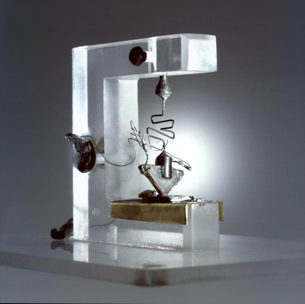
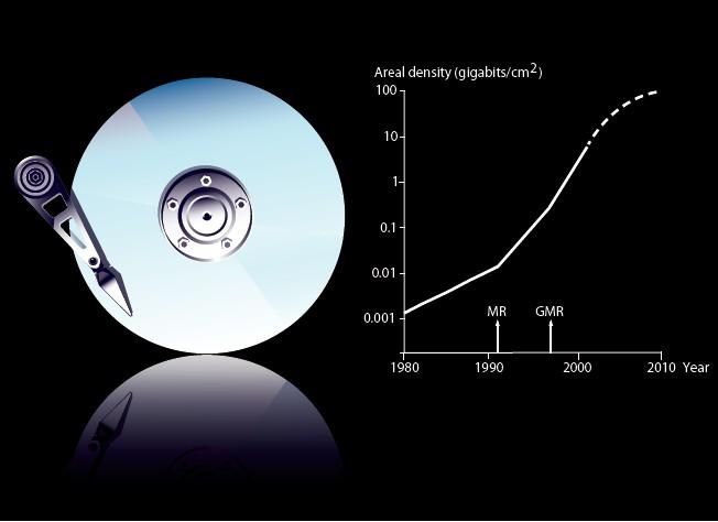
6 The birth of nonotechnology/spintronics Nobel Prize 2007: Albert Fert & Peter Gruenberg For the discovery of Giant Magnetoresistance
7
8 Chapter 3. Junctions & Contacts 3.1 Metal-semiconductor contacts A review of the principles Idealized metal-semiconductor junctions Current-Voltage characteristics Ohmic contacts 3.2 p-n junctions 3.3 Heterojunctions
9 Separated M-S Systems
10 Bring M-S into Contact f D1, 2 = 1 1 exp [ E E f1, 2 / kt ] E f1=e f2 At thermal equilibrium the Fermi levels is constant throughout a system.
11 Inhomogeneously Doped SC E0 E0 Ec Ef Ec Ei Ef Ei Ev Ev
12 Inhomogeneously Doped SC
13 Ideal Density-of-States Typical Metal Typical Semiconductor
14 Energy levels
15 Charge Transfer Equilibrium Electrons depleted Assume band structures not changed near the surface. Real situation: Surface states
16 No Hope to Solve Analytically Poisson s equation 2 d q q = = p n N N, n=n exp d a i 2 kt dx s s the electron density, the hole density and the donor and acceptor densities. To solve the equation, we have to express the electron and hole density, n and p, as a function of the potential, φ 2 d q q = 2 n sinh N N i a d 2 kt dx s { } { } E f E i E f Ei E i E f n=ni exp, p=ni exp, = kbt kbt q
17 Depletion Approximation For the idealized n-type semiconductor, hole density neglected Electron density n << Nd, thus depleted, from the interface to x = xd Beyond xd, n = Nd Negative charge right at the metal surface
18 Field, Potential and Charge (Gauss law)
19 Applied Bias Up to this point, we have been considering thermal equilibrium conditions at the metal-semiconductor junction. Now, we study the case of an applied voltage; i.e., a nonequilibrium condition. Electrons transferring from metal to semiconductor see a barrier.

20 Applied Bias To the first order, the barrier height is independent of bias because no voltage can be sustained across the metal. Bias changes the curvature of the semiconductor bands, modifying the potential drop from φi.
21 Junction Charge & Capacitor
22 Small-Signal Capacitance
23 Variable Doping
24 Semiconductor Profiler
25 Schottky Barrier Lowering We now explore the statement that the barrier to electron flow from metal to semiconductor is to first order unchanged by bias. Approximations: Free electron theory Metal as plane conducting sheet Semiconductor: effective mass, relative permittivity Root: Metal plane = image charge of opposite sign
26 Schottky Barrier Lowering
27 I-V Characteristics w/out Math At equilibrium, rate at which electrons cross the barrier into the semiconductor is balanced by rate at which electrons cross the barrier into the metal. (flow = counter flow). When a bias is applied, the potential drop within the semiconductor is changed and we can expect the flux of electrons from the semiconductor toward the metal to be modified. The flux of electrons from the metal to the semiconductor is not affected. The difference is the net current.
28 I-V Characteristics The current of electrons from the semiconductor to the metal is proportional to the density of electrons at the boundary. q B q i n s = N C exp = N D exp kt kt q B =q i E C E f In equilibrium, q i J MS = J SM =K N D exp KT
29 I-V Characteristics When a bias is applied to the junction, q i V a n s = N D exp kt Now, q i V a q i J =J MS J SM = K N D exp K N D exp KT KT Therefore, the ideal diode equation reads [ ] qv a J =J 0 exp 1 KT
30 Comments The ideal diode equation arises when a barrier to electron flow affects the thermal flux of carriers asymmetrically. The essence of the ideal diode equation predicts a saturation current J0 for negative Va and a very large steeply rising current when Va is positive. J0 in the above ideal case is independent of the applied bias. More careful analysis will modify this slightly.
31 More Detailed Analysis Schottky: Integrating the equations for carrier diffusion and drift across the depletion region near the contact. Assumes that the dimensions of the space-charge region are sufficiently large (a few electron mean-free path) so that the use of a diffusion constant and a mobility value are meaningful (small field, no drift velocity saturation). Bethe: Based on carrier emission from the metal. Valid even when these abovementioned constraints are not met.
32 Diffusion and Drift Currents [ J x =q n n E x D n ] [ dn qn d dn =q D n dx kt dx dx ]
33 Trick for Integration [ J x =q n n E x D n xd J x 0 exp ] [ dn qn d dn =q Dn dx kt dx dx [ ] q q dx=q D n n exp kt kt ] xd 0 0 =0 ; x d = i V a = B n V a q B q n n 0 = N C exp ; n x d =N D =N C exp kt kt J x= q B q D n N C exp kt xd 0 ] [ ] [ q x exp dx kt qv a qv a exp 1 = J 0 exp 1 kt kt
34 Schottky Barrier
35 Mott Barrier
36 Comments One important implicit assumption is that the system is in quasiequilibrium, i.e., almost at thermal equilibrium even though currents are flowing. Electron density at the interface when the bias is applied. Using Einstein relation to relate drift and diffusion current. The ultimate test: Agreements between measurements and predictions. Derivation not valid when Va ~ φi (no barrier). A fraction of the voltage is dropped across the resistance of the semiconductor. The forward voltage across the junction is reduced.
37 Schottky Diodes
38 Surface Effects
39 Pinning of Fermi Energy To account for the surface effects, the metal-semiconductor contact is treated as if it contained an intermediate region sandwiched between the two crystals. For a large density of surface states, the Fermi energy is said to be pinned by the high density of states.
40 Nonrectifying (Ohmic) Contacts Definition: The contact itself offers negligible resistance to current flow when compared to the bulk. The voltage dropped across the ohmic contacts is negligible compared to voltage drops elsewhere in the device. No power is dissipated in the contacts. Ohmic contacts can be described as being in equilibrium even in when currents are flowing. All free-carrier densities at an Ohmic contact are unchanged by current flow. The densities remain at their thermal-equilibrium values.
41 Tunneling Contacts By heavily doping the semiconductor, so that the barrier width is very small and tunneling through the barrier can take place.
42 Schottky Ohmic Contacts
43 Chapter 3. Junctions & Contacts 3.1 Metal-semiconductor contacts 3.2 p-n junctions 3.3 Heterojunctions
44 Metal-Semiconductor Contacts A system of electrons is characterized by a constant Fermi level at thermal equilibrium. Systems that are not in thermal equilibrium approach equilibrium as electrons are transferred from regions with a higher Fermi level to regions with a lower Fermi level. The transferred charge causes the buildup of barriers against further flow, and the potential drop across these barriers increases to a value that just equalizes the Fermi levels. Similar phenomena in a single crystal with non-uniform doping.
45 p-n Junction E0 E0 electrons Ec Ec Ef Ei Ei Ef Ev Ev Systems that are not in thermal equilibrium approach equilibrium as electrons are transferred from regions with a higher Fermi level to regions with a lower Fermi level.
46 p-n Junction E0 Ec Ei Ef Ev E0 E Ec Ef Ei Ev A system of electrons is characterized by a constant Fermi level at thermal equilibrium.
47 p-n Junction E0 Ec Ei Ef Ev φi E0 Ec Ef Ei Ev The transferred charge causes the buildup of barriers against further flow, and the potential drop across these barriers increases to a value that just equalizes the Fermi levels
48 Graded Impurity Distributions We assume initially the majority carrier density equals the dopant density everywhere. We ask how equilibrium is approached. A gradient in the mobile carrier density diffusion of carriers. Carrier diffusion leaves dopant ions behind. Separation of charge field opposing the diffusion flow. Equilibrium is reached when diffusion is balanced by the field.
49 Potential The separation of the Fermi level from the conduction-band edge (or intrinsic Fermi level) represents the potential energy of an electron.
50 Field dn J n=q n n x q D n =0 in equilibrium dx Using mass-action law,
51 Density vs Potential Barrier
52 Poisson s Equation 2 d q = = p n N d N a 2 s s dx q q n=ni exp ; p=ni exp kt kt 2 d q q = 2 ni sinh N a N d 2 s kt dx Cannot be solved in the general case!

53 (i) Small Gradient Case Quasi-neutrality approx.: constant field: kt qλ
54 (ii) p-n Junction Depletion approximation quasi-neutral approximation
55 Depletion of Mobile Charge
56 Potential Barrier p = Na n= 2 i n Na p= 0 n= 0 d 2φ q = ( Nd Na ) 2 dx εs n = Nd p= ni2 Nd
57 Two Idealized Cases Linearly graded junction: a continuous gradient in dopant between n-type and p-type regions. Step junction (abrupt junction): a constant n-type dopant density changes abruptly to a constant p-type dopant density for example, formed by epitaxial deposition
58 Step Junctions
59 Step Junction Analysis In n-type region, Integration leads to Similarly, Continuation at x = 0 requires This is just the charge neutrality in the depletion region.
60 Step Junction Analysis In n-type region, In p-type region, Totally,
61 Comments At high dopant concentrations, use F-D distribution in stead. However, the practical result is that the Fermi level is very near the band edge. For example, for heavily doped p-type silicon and lightly doped silicon: Total depletion-region width is: There is only partial depletion near the edge of the depletion region.
62 Partial Depletion
63 Debye Length 16 3 Typically, N d ~10 cm, L D ~40 nm
64 Linearly Graded Junction

65 Do It Yourself!
66 Applied Bias Everything works as before. Just replace φ i by φ i Va For positive Va, the barrier to the majority carrier is reduced; depletion region is narrowed; the junction is forward biased; appreciable currents can flow under small forward bias. For negative Va, the barrier to the majority carrier increases; depletion region widens; the junction is reverse biased; there is very little current flow under reverse bias.
67 Depletion Width & Maximum Field Abrupt p-n junction Linearly graded junction
68 Capacitance
69 Varactor Under reverse bias VR C i V R n Question: Which one is more sensitive? Linearly graded junction? Or abrupt junction? LGJ: n = 1/3 AJ: n = 1/2 (more sensitive) Can you design an even more sensitive varactor?
70 Junction Breakdown
71 Avalanche Breakdown Q: Conservation of energy and momentum requires the original electron possess kinetic energy of at least? 3 Eg 2 Avalanche breakdown is confines to the central portion of the space-charge region, where the field is sizeable.
72 Zener Breakdown The WKB approximation
73 Currents in p-n junctions Generation and recombination Continuity equation Current-voltage characteristics Charge storage and diode transients

74 Recombination through Traps Additional reading: Shockley-Hall-Read recombination
75 Generation and Recombination Recombination rate: n ' n n0 U= = τn τn Excess carrier concentration Carrier lifetime
76 Minority Carriers Matter Quasi-neutral zone Quasi-neutral zone ==> current flow (I-V characteristics) & charge storage (transient behavior)

77 Ideal-Diode Analysis Consider excess holes injected into the n-regions, where bulk recombination through generation-recombination centers is dominant. 2 pn pn pn E = pn p p E D p G p R p 2 t x x x In the quasi-neutral region, we have roughly E = 0. 2 pn p n pn p n0 =Dp 2 p t x Stationary:
78 Minority-Carrier Boundary Values Change of majority-carrier populations negligible. Detailed balance nearly applied for small enough applied bias. φi
79 Minority-Carrier Boundary Values Change of majority-carrier populations negligible. Detailed balance nearly applied for small enough applied bias.
80 Case 1: Long-Base Diode Length scale: diffusion length Lp
81 Hole Current
82 Total Current Minority-carrier electron current injected into p-region: Total current:
83 Case 2: Short-Base Diode Length scale: lengths of n- and p-type regions, WB and WE Ohmic contact

84 Current Assumption: No recombination occurs in n-type region. Hole current through n-type region: Total current:
85 Higher Order Corrections The ideal-diode equation is based on events in the quasi-neutral regions. The space-charge region is purely a barrier to diffusion of majority carriers and it plays a role only in the establishment of minority-carrier density at its boundaries. This is a reasonable first-order description of all the events. It is inaccurate, especially for silicon p-n junctions. Corrections due to events in the space-charge region are required.
86 Qualitative Picture
87 Diode Transients On: buildup time = stored charge / source current Off: turn-off time limited by how fast charge can be removed from the quasineutral region.
88 Charge Storage Mechanism 1: Majority carriers near the edges of the depletion region move as the depletion region expands or contracts in response to a changing bias. The charge storage in the depletion region is modeled by a small-signal capacitance, e.g., the abruptjunction depletion capacitance. Mechanism 2: Minority-carrier charge changes in the quasi-neutral region when applied bias is switched on or off. This can be modeled by another small-signal capacitance - diffusion capacitance. Equivalent circuit
89 Chapter 3. Junctions & Contacts 3.1 Metal-semiconductor contacts 3.2 p-n junctions 3.3 Heterojunctions
90 Will be discussed in the preparation of twodimensional electron gas.
Chapter 7. The pn Junction
 Chapter 7 The pn Junction Chapter 7 PN Junction PN junction can be fabricated by implanting or diffusing donors into a P-type substrate such that a layer of semiconductor is converted into N type. Converting
Session 6: Solid State Physics. Diode
 Session 6: Solid State Physics Diode 1 Outline A B C D E F G H I J 2 Definitions / Assumptions Homojunction: the junction is between two regions of the same material Heterojunction: the junction is between
Semiconductor Physics fall 2012 problems
 Semiconductor Physics fall 2012 problems 1. An n-type sample of silicon has a uniform density N D = 10 16 atoms cm -3 of arsenic, and a p-type silicon sample has N A = 10 15 atoms cm -3 of boron. For each
Consider a uniformly doped PN junction, in which one region of the semiconductor is uniformly doped with acceptor atoms and the adjacent region is
 CHAPTER 7 The PN Junction Consider a uniformly doped PN junction, in which one region of the semiconductor is uniformly doped with acceptor atoms and the adjacent region is uniformly doped with donor atoms.
Review Energy Bands Carrier Density & Mobility Carrier Transport Generation and Recombination
 Review Energy Bands Carrier Density & Mobility Carrier Transport Generation and Recombination The Metal-Semiconductor Junction: Review Energy band diagram of the metal and the semiconductor before (a)
CHAPTER 4: P-N P N JUNCTION Part 2. M.N.A. Halif & S.N. Sabki
 CHAPTER 4: P-N P N JUNCTION Part 2 Part 2 Charge Storage & Transient Behavior Junction Breakdown Heterojunction CHARGE STORAGE & TRANSIENT BEHAVIOR Once injected across the junction, the minority carriers
Semiconductor Physics fall 2012 problems
 Semiconductor Physics fall 2012 problems 1. An n-type sample of silicon has a uniform density N D = 10 16 atoms cm -3 of arsenic, and a p-type silicon sample has N A = 10 15 atoms cm -3 of boron. For each
For the following statements, mark ( ) for true statement and (X) for wrong statement and correct it.
 for true statement and (X) for wrong statement and correct it.") Benha University Faculty of Engineering Shoubra Electrical Engineering Department First Year communications. Answer all the following questions Illustrate your answers with sketches when necessary. The
Benha University Faculty of Engineering Shoubra Electrical Engineering Department First Year communications. Answer all the following questions Illustrate your answers with sketches when necessary. The
ECE 340 Lecture 27 : Junction Capacitance Class Outline:
 ECE 340 Lecture 27 : Junction Capacitance Class Outline: Breakdown Review Junction Capacitance Things you should know when you leave M.J. Gilbert ECE 340 Lecture 27 10/24/11 Key Questions What types of
Schottky Rectifiers Zheng Yang (ERF 3017,
 ECE442 Power Semiconductor Devices and Integrated Circuits Schottky Rectifiers Zheng Yang (ERF 3017, email: yangzhen@uic.edu) Power Schottky Rectifier Structure 2 Metal-Semiconductor Contact The work function
Metal Semiconductor Contacts
 Metal Semiconductor Contacts The investigation of rectification in metal-semiconductor contacts was first described by Braun [33-35], who discovered in 1874 the asymmetric nature of electrical conduction
PHYSICAL ELECTRONICS(ECE3540) CHAPTER 9 METAL SEMICONDUCTOR AND SEMICONDUCTOR HETERO-JUNCTIONS
 CHAPTER 9 METAL SEMICONDUCTOR AND SEMICONDUCTOR HETERO-JUNCTIONS") PHYSICAL ELECTRONICS(ECE3540) CHAPTER 9 METAL SEMICONDUCTOR AND SEMICONDUCTOR HETERO-JUNCTIONS Tennessee Technological University Monday, November 11, 013 1 Introduction Chapter 4: we considered the semiconductor
PHYSICAL ELECTRONICS(ECE3540) CHAPTER 9 METAL SEMICONDUCTOR AND SEMICONDUCTOR HETERO-JUNCTIONS Tennessee Technological University Monday, November 11, 013 1 Introduction Chapter 4: we considered the semiconductor
PHYSICAL ELECTRONICS(ECE3540) CHAPTER 9 METAL SEMICONDUCTOR AND SEMICONDUCTOR HETERO-JUNCTIONS
 CHAPTER 9 METAL SEMICONDUCTOR AND SEMICONDUCTOR HETERO-JUNCTIONS") PHYSICAL ELECTRONICS(ECE3540) CHAPTER 9 METAL SEMICONDUCTOR AND SEMICONDUCTOR HETERO-JUNCTIONS Tennessee Technological University Wednesday, October 30, 013 1 Introduction Chapter 4: we considered the
PHYSICAL ELECTRONICS(ECE3540) CHAPTER 9 METAL SEMICONDUCTOR AND SEMICONDUCTOR HETERO-JUNCTIONS Tennessee Technological University Wednesday, October 30, 013 1 Introduction Chapter 4: we considered the
1 Name: Student number: DEPARTMENT OF PHYSICS AND PHYSICAL OCEANOGRAPHY MEMORIAL UNIVERSITY OF NEWFOUNDLAND. Fall :00-11:00
 1 Name: DEPARTMENT OF PHYSICS AND PHYSICAL OCEANOGRAPHY MEMORIAL UNIVERSITY OF NEWFOUNDLAND Final Exam Physics 3000 December 11, 2012 Fall 2012 9:00-11:00 INSTRUCTIONS: 1. Answer all seven (7) questions.
Semiconductor Physics Problems 2015
 Semiconductor Physics Problems 2015 Page and figure numbers refer to Semiconductor Devices Physics and Technology, 3rd edition, by SM Sze and M-K Lee 1. The purest semiconductor crystals it is possible
Diodes. anode. cathode. cut-off. Can be approximated by a piecewise-linear-like characteristic. Lecture 9-1
 Diodes mplest nonlinear circuit element Basic operation sets the foundation for Bipolar Junction Transistors (BJTs) Also present in Field Effect Transistors (FETs) Ideal diode characteristic anode cathode
Semiconductor Junctions
 8 Semiconductor Junctions Almost all solar cells contain junctions between different materials of different doping. Since these junctions are crucial to the operation of the solar cell, we will discuss
Semiconductor Physics. Lecture 6
 Semiconductor Physics Lecture 6 Recap pn junction and the depletion region Driven by the need to have no gradient in the fermi level free carriers migrate across the pn junction leaving a region with few
Effective masses in semiconductors
 Effective masses in semiconductors The effective mass is defined as: In a solid, the electron (hole) effective mass represents how electrons move in an applied field. The effective mass reflects the inverse
Current mechanisms Exam January 27, 2012
 Current mechanisms Exam January 27, 2012 There are four mechanisms that typically cause currents to flow: thermionic emission, diffusion, drift, and tunneling. Explain briefly which kind of current mechanisms
Peak Electric Field. Junction breakdown occurs when the peak electric field in the PN junction reaches a critical value. For the N + P junction,
 Peak Electric Field Junction breakdown occurs when the peak electric field in the P junction reaches a critical value. For the + P junction, qa E ( x) ( xp x), s W dep 2 s ( bi Vr ) 2 s potential barrier
EECS130 Integrated Circuit Devices
 EECS130 Integrated Circuit Devices Professor Ali Javey 10/02/2007 MS Junctions, Lecture 2 MOS Cap, Lecture 1 Reading: finish chapter14, start chapter16 Announcements Professor Javey will hold his OH at
ECE 340 Lecture 21 : P-N Junction II Class Outline:
 ECE 340 Lecture 21 : P-N Junction II Class Outline: Contact Potential Equilibrium Fermi Levels Things you should know when you leave Key Questions What is the contact potential? Where does the transition
This is the 15th lecture of this course in which we begin a new topic, Excess Carriers. This topic will be covered in two lectures.
 Solid State Devices Dr. S. Karmalkar Department of Electronics and Communication Engineering Indian Institute of Technology, Madras Lecture - 15 Excess Carriers This is the 15th lecture of this course
Midterm I - Solutions
 UNIVERSITY OF CALIFORNIA College of Engineering Department of Electrical Engineering and Computer Sciences EECS 130 Spring 2008 Professor Chenming Hu Midterm I - Solutions Name: SID: Grad/Undergrad: Closed
EECS130 Integrated Circuit Devices
 EECS130 Integrated Circuit Devices Professor Ali Javey 9/18/2007 P Junctions Lecture 1 Reading: Chapter 5 Announcements For THIS WEEK OLY, Prof. Javey's office hours will be held on Tuesday, Sept 18 3:30-4:30
Lecture 15 - The pn Junction Diode (I) I-V Characteristics. November 1, 2005
 I-V Characteristics. November 1, 2005") 6.012 - Microelectronic Devices and Circuits - Fall 2005 Lecture 15-1 Lecture 15 - The pn Junction Diode (I) I-V Characteristics November 1, 2005 Contents: 1. pn junction under bias 2. I-V characteristics
6.012 - Microelectronic Devices and Circuits - Fall 2005 Lecture 15-1 Lecture 15 - The pn Junction Diode (I) I-V Characteristics November 1, 2005 Contents: 1. pn junction under bias 2. I-V characteristics
Solid State Electronics. Final Examination
 The University of Toledo EECS:4400/5400/7400 Solid State Electronic Section elssf08fs.fm - 1 Solid State Electronics Final Examination Problems Points 1. 1. 14 3. 14 Total 40 Was the exam fair? yes no
pn JUNCTION THE SHOCKLEY MODEL
 The pn Junction: The Shockley Model ( S. O. Kasap, 1990-001) 1 pn JUNCTION THE SHOCKLEY MODEL Safa Kasap Department of Electrical Engineering University of Saskatchewan Canada Although the hole and its
Sheng S. Li. Semiconductor Physical Electronics. Second Edition. With 230 Figures. 4) Springer
 Springer") Sheng S. Li Semiconductor Physical Electronics Second Edition With 230 Figures 4) Springer Contents Preface 1. Classification of Solids and Crystal Structure 1 1.1 Introduction 1 1.2 The Bravais Lattice
Sheng S. Li Semiconductor Physical Electronics Second Edition With 230 Figures 4) Springer Contents Preface 1. Classification of Solids and Crystal Structure 1 1.1 Introduction 1 1.2 The Bravais Lattice
( )! N D ( x) ) and equilibrium
! N D ( x) ) and equilibrium") ECE 66: SOLUTIONS: ECE 66 Homework Week 8 Mark Lundstrom March 7, 13 1) The doping profile for an n- type silicon wafer ( N D = 1 15 cm - 3 ) with a heavily doped thin layer at the surface (surface concentration,
ECE 66: SOLUTIONS: ECE 66 Homework Week 8 Mark Lundstrom March 7, 13 1) The doping profile for an n- type silicon wafer ( N D = 1 15 cm - 3 ) with a heavily doped thin layer at the surface (surface concentration,
Final Examination EE 130 December 16, 1997 Time allotted: 180 minutes
 Final Examination EE 130 December 16, 1997 Time allotted: 180 minutes Problem 1: Semiconductor Fundamentals [30 points] A uniformly doped silicon sample of length 100µm and cross-sectional area 100µm 2
Semiconductor Physics and Devices
 The pn Junction 1) Charge carriers crossing the junction. 3) Barrier potential Semiconductor Physics and Devices Chapter 8. The pn Junction Diode 2) Formation of positive and negative ions. 4) Formation
junctions produce nonlinear current voltage characteristics which can be exploited
 Chapter 6 P-N DODES Junctions between n-and p-type semiconductors are extremely important foravariety of devices. Diodes based on p-n junctions produce nonlinear current voltage characteristics which can
Quiz #1 Practice Problem Set
 Name: Student Number: ELEC 3908 Physical Electronics Quiz #1 Practice Problem Set? Minutes January 22, 2016 - No aids except a non-programmable calculator - All questions must be answered - All questions
Lecture 16 - The pn Junction Diode (II) Equivalent Circuit Model. April 8, 2003
 Equivalent Circuit Model. April 8, 2003") 6.012 - Microelectronic Devices and Circuits - Spring 2003 Lecture 16-1 Lecture 16 - The pn Junction Diode (II) Equivalent Circuit Model April 8, 2003 Contents: 1. I-V characteristics (cont.) 2. Small-signal
6.012 - Microelectronic Devices and Circuits - Spring 2003 Lecture 16-1 Lecture 16 - The pn Junction Diode (II) Equivalent Circuit Model April 8, 2003 Contents: 1. I-V characteristics (cont.) 2. Small-signal
Avalanche breakdown. Impact ionization causes an avalanche of current. Occurs at low doping
 Avalanche breakdown Impact ionization causes an avalanche of current Occurs at low doping Zener tunneling Electrons tunnel from valence band to conduction band Occurs at high doping Tunneling wave decays
n N D n p = n i p N A
 Summary of electron and hole concentration in semiconductors Intrinsic semiconductor: E G n kt i = pi = N e 2 0 Donor-doped semiconductor: n N D where N D is the concentration of donor impurity Acceptor-doped
Semiconductor Device Physics
 1 emiconductor Device Physics Lecture 8 http://zitompul.wordpress.com 2 0 1 3 emiconductor Device Physics 2 M Contacts and chottky Diodes 3 M Contact The metal-semiconductor (M) contact plays a very important
PN Junction and MOS structure
 PN Junction and MOS structure Basic electrostatic equations We will use simple one-dimensional electrostatic equations to develop insight and basic understanding of how semiconductor devices operate Gauss's
ECE-305: Spring 2018 Exam 2 Review
 ECE-305: Spring 018 Exam Review Pierret, Semiconductor Device Fundamentals (SDF) Chapter 3 (pp. 75-138) Chapter 5 (pp. 195-6) Professor Peter Bermel Electrical and Computer Engineering Purdue University,
6.012 Electronic Devices and Circuits
 Page 1 of 1 YOUR NAME Department of Electrical Engineering and Computer Science Massachusetts Institute of Technology 6.12 Electronic Devices and Circuits Exam No. 1 Wednesday, October 7, 29 7:3 to 9:3
Semiconductor Physics. Lecture 3
 Semiconductor Physics Lecture 3 Intrinsic carrier density Intrinsic carrier density Law of mass action Valid also if we add an impurity which either donates extra electrons or holes the number of carriers
PN Junctions. Lecture 7
 Lecture 7 PN Junctions Kathy Aidala Applied Physics, G2 Harvard University 10 October, 2002 Wei 1 Active Circuit Elements Why are they desirable? Much greater flexibility in circuit applications. What
Appendix 1: List of symbols
 Appendix 1: List of symbols Symbol Description MKS Units a Acceleration m/s 2 a 0 Bohr radius m A Area m 2 A* Richardson constant m/s A C Collector area m 2 A E Emitter area m 2 b Bimolecular recombination
Sample Exam # 2 ECEN 3320 Fall 2013 Semiconductor Devices October 28, 2013 Due November 4, 2013
 Sample Exam # 2 ECEN 3320 Fall 203 Semiconductor Devices October 28, 203 Due November 4, 203. Below is the capacitance-voltage curve measured from a Schottky contact made on GaAs at T 300 K. Figure : Capacitance
ECE 440 Lecture 28 : P-N Junction II Class Outline:
 ECE 440 Lecture 28 : P-N Junction II Class Outline: Contact Potential Equilibrium Fermi Levels Things you should know when you leave Key Questions What is the contact potential? Where does the transition
MTLE-6120: Advanced Electronic Properties of Materials. Semiconductor p-n junction diodes. Reading: Kasap ,
 MTLE-6120: Advanced Electronic Properties of Materials 1 Semiconductor p-n junction diodes Reading: Kasap 6.1-6.5, 6.9-6.12 Metal-semiconductor contact potential 2 p-type n-type p-type n-type Same semiconductor
Lecture 17 - p-n Junction. October 11, Ideal p-n junction in equilibrium 2. Ideal p-n junction out of equilibrium
 6.72J/3.43J - Integrated Microelectronic Devices - Fall 22 Lecture 17-1 Lecture 17 - p-n Junction October 11, 22 Contents: 1. Ideal p-n junction in equilibrium 2. Ideal p-n junction out of equilibrium
Section 12: Intro to Devices
 Section 12: Intro to Devices Extensive reading materials on reserve, including Robert F. Pierret, Semiconductor Device Fundamentals EE143 Ali Javey Bond Model of Electrons and Holes Si Si Si Si Si Si Si
ECE 440 Lecture 20 : PN Junction Electrostatics II Class Outline:
 ECE 440 Lecture 20 : PN Junction Electrostatics II Class Outline: Depletion Approximation Step Junction Things you should know when you leave Key Questions What is the space charge region? What are the
UNIVERSITY OF CALIFORNIA College of Engineering Department of Electrical Engineering and Computer Sciences. EECS 130 Professor Ali Javey Fall 2006
 UNIVERSITY OF CALIFORNIA College of Engineering Department of Electrical Engineering and Computer Sciences EECS 130 Professor Ali Javey Fall 2006 Midterm I Name: Closed book. One sheet of notes is allowed.
Semiconductor Physical Electronics
 Semiconductor Physical Electronics Sheng S. Li Department of Electrical Engineering University of Florida Gainesville, Florida Plenum Press New York and London Contents CHAPTER 1. Classification of Solids
Semiconductor device structures are traditionally divided into homojunction devices
 0. Introduction: Semiconductor device structures are traditionally divided into homojunction devices (devices consisting of only one type of semiconductor material) and heterojunction devices (consisting
ESE 372 / Spring 2013 / Lecture 5 Metal Oxide Semiconductor Field Effect Transistor
 Metal Oxide Semiconductor Field Effect Transistor V G V G 1 Metal Oxide Semiconductor Field Effect Transistor We will need to understand how this current flows through Si What is electric current? 2 Back
Charge Carriers in Semiconductor
 Charge Carriers in Semiconductor To understand PN junction s IV characteristics, it is important to understand charge carriers behavior in solids, how to modify carrier densities, and different mechanisms
Electronic Devices and Circuits Lecture 5 - p-n Junction Injection and Flow - Outline
 6.012 - Electronic Devices and Circuits Lecture 5 - p-n Junction Injection and Flow - Outline Review Depletion approimation for an abrupt p-n junction Depletion charge storage and depletion capacitance
Schottky diodes. JFETs - MESFETs - MODFETs
 Technische Universität Graz Institute of Solid State Physics Schottky diodes JFETs - MESFETs - MODFETs Quasi Fermi level When the charge carriers are not in equilibrium the Fermi energy can be different
Lecture 19 - p-n Junction (cont.) October 18, Ideal p-n junction out of equilibrium (cont.) 2. pn junction diode: parasitics, dynamics
 October 18, Ideal p-n junction out of equilibrium (cont.) 2. pn junction diode: parasitics, dynamics") 6.720J/3.43J - Integrated Microelectronic Devices - Fall 2002 Lecture 19-1 Lecture 19 - p-n Junction (cont.) October 18, 2002 Contents: 1. Ideal p-n junction out of equilibrium (cont.) 2. pn junction diode:
6.720J/3.43J - Integrated Microelectronic Devices - Fall 2002 Lecture 19-1 Lecture 19 - p-n Junction (cont.) October 18, 2002 Contents: 1. Ideal p-n junction out of equilibrium (cont.) 2. pn junction diode:
collisions of electrons. In semiconductor, in certain temperature ranges the conductivity increases rapidly by increasing temperature
 1.9. Temperature Dependence of Semiconductor Conductivity Such dependence is one most important in semiconductor. In metals, Conductivity decreases by increasing temperature due to greater frequency of
3. Two-dimensional systems
 3. Two-dimensional systems Image from IBM-Almaden 1 Introduction Type I: natural layered structures, e.g., graphite (with C nanostructures) Type II: artificial structures, heterojunctions Great technological
PN Junction
 P Junction 2017-05-04 Definition Power Electronics = semiconductor switches are used Analogue amplifier = high power loss 250 200 u x 150 100 u Udc i 50 0 0 50 100 150 200 250 300 350 400 i,u dc i,u u
Section 12: Intro to Devices
 Section 12: Intro to Devices Extensive reading materials on reserve, including Robert F. Pierret, Semiconductor Device Fundamentals Bond Model of Electrons and Holes Si Si Si Si Si Si Si Si Si Silicon
Solid State Physics SEMICONDUCTORS - IV. Lecture 25. A.H. Harker. Physics and Astronomy UCL
 Solid State Physics SEMICONDUCTORS - IV Lecture 25 A.H. Harker Physics and Astronomy UCL 9.9 Carrier diffusion and recombination Suppose we have a p-type semiconductor, i.e. n h >> n e. (1) Create a local
Figure 3.1 (p. 141) Figure 3.2 (p. 142)
 Figure 3.2 (p. 142)") Figure 3.1 (p. 141) Allowed electronic-energy-state systems for two isolated materials. States marked with an X are filled; those unmarked are empty. System 1 is a qualitative representation of a metal;
Figure 3.1 (p. 141) Allowed electronic-energy-state systems for two isolated materials. States marked with an X are filled; those unmarked are empty. System 1 is a qualitative representation of a metal;
EE 3329 Electronic Devices Syllabus ( Extended Play )
") EE 3329 - Electronic Devices Syllabus EE 3329 Electronic Devices Syllabus ( Extended Play ) The University of Texas at El Paso The following concepts can be part of the syllabus for the Electronic Devices
EE 3329 - Electronic Devices Syllabus EE 3329 Electronic Devices Syllabus ( Extended Play ) The University of Texas at El Paso The following concepts can be part of the syllabus for the Electronic Devices
Spring Semester 2012 Final Exam
 Spring Semester 2012 Final Exam Note: Show your work, underline results, and always show units. Official exam time: 2.0 hours; an extension of at least 1.0 hour will be granted to anyone. Materials parameters
The 5 basic equations of semiconductor device physics: We will in general be faced with finding 5 quantities:
 6.012 - Electronic Devices and Circuits Solving the 5 basic equations - 2/12/08 Version The 5 basic equations of semiconductor device physics: We will in general be faced with finding 5 quantities: n(x,t),
UNIVERSITY OF CALIFORNIA College of Engineering Department of Electrical Engineering and Computer Sciences. Professor Chenming Hu.
 UNIVERSITY OF CALIFORNIA College of Engineering Department of Electrical Engineering and Computer Sciences EECS 130 Spring 2009 Professor Chenming Hu Midterm I Name: Closed book. One sheet of notes is
BJT - Mode of Operations
 JT - Mode of Operations JTs can be modeled by two back-to-back diodes. N+ P N- N+ JTs are operated in four modes. HO #6: LN 251 - JT M Models Page 1 1) Forward active / normal junction forward biased junction
Lecture 16 The pn Junction Diode (III)
") Lecture 16 The pn Junction iode (III) Outline I V Characteristics (Review) Small signal equivalent circuit model Carrier charge storage iffusion capacitance Reading Assignment: Howe and Sodini; Chapter
Lecture 16 The pn Junction iode (III) Outline I V Characteristics (Review) Small signal equivalent circuit model Carrier charge storage iffusion capacitance Reading Assignment: Howe and Sodini; Chapter
GaN based transistors
 GaN based transistors S FP FP dielectric G SiO 2 Al x Ga 1-x N barrier i-gan Buffer i-sic D Transistors "The Transistor was probably the most important invention of the 20th Century The American Institute
Basic Physics of Semiconductors
 Basic Physics of Semiconductors Semiconductor materials and their properties PN-junction diodes Reverse Breakdown EEM 205 Electronics I Dicle University, EEE Dr. Mehmet Siraç ÖZERDEM Semiconductor Physics
8. Schottky contacts / JFETs
 Technische Universität Graz Institute of Solid State Physics 8. Schottky contacts / JFETs Nov. 21, 2018 Technische Universität Graz Institute of Solid State Physics metal - semiconductor contacts Photoelectric
Lecture (02) PN Junctions and Diodes
 PN Junctions and Diodes") Lecture (02) PN Junctions and Diodes By: Dr. Ahmed ElShafee ١ I Agenda N type, P type semiconductors N Type Semiconductor P Type Semiconductor PN junction Energy Diagrams of the PN Junction and Depletion
Lecture (02) PN Junctions and Diodes By: Dr. Ahmed ElShafee ١ I Agenda N type, P type semiconductors N Type Semiconductor P Type Semiconductor PN junction Energy Diagrams of the PN Junction and Depletion
Nature of Lesson (Lecture/Tutorial) H3 WK No. Day/ Date. Remarks. Duration. 4.00pm 6.30pm ALL. 2.5 hours. Introduction to Semiconductors Lecture 01
 H3 WK No. Day/ Date. Remarks. Duration. 4.00pm 6.30pm ALL. 2.5 hours. Introduction to Semiconductors Lecture 01") JANUARY 2018 INTAKE Subject : Semiconductor Physics & Devices Venue : HCI Schedule : Mondays for Tutorial (3pm 5pm / 5pm 7pm) or Tuesdays for Tutorial (3pm 5pm / 5pm 7pm) and Thursdays for Lecture (4pm-6.30
JANUARY 2018 INTAKE Subject : Semiconductor Physics & Devices Venue : HCI Schedule : Mondays for Tutorial (3pm 5pm / 5pm 7pm) or Tuesdays for Tutorial (3pm 5pm / 5pm 7pm) and Thursdays for Lecture (4pm-6.30
Schottky Diodes (M-S Contacts)
") Schottky Diodes (M-S Contacts) Three MITs of the Day Band diagrams for ohmic and rectifying Schottky contacts Similarity to and difference from bipolar junctions on electrostatic and IV characteristics.
Schottky Diodes (M-S Contacts) Three MITs of the Day Band diagrams for ohmic and rectifying Schottky contacts Similarity to and difference from bipolar junctions on electrostatic and IV characteristics.
Fundamentals of the Metal Oxide Semiconductor Field-Effect Transistor
 Triode Working FET Fundamentals of the Metal Oxide Semiconductor Field-Effect Transistor The characteristics of energy bands as a function of applied voltage. Surface inversion. The expression for the
Lecture 5 Junction characterisation
 Lecture 5 Junction characterisation Jon Major October 2018 The PV research cycle Make cells Measure cells Despair Repeat 40 1.1% 4.9% Data Current density (ma/cm 2 ) 20 0-20 -1.0-0.5 0.0 0.5 1.0 Voltage
The pn junction. [Fonstad, Ghione]
![The pn junction. [Fonstad, Ghione]](/thumbs/93/112370833.jpg "The pn junction. [Fonstad, Ghione]") The pn junction [Fonstad, Ghione] Band diagram On the vertical axis: potential energy of the electrons On the horizontal axis: now there is nothing: later we ll put the position qf s : work function (F
The pn junction [Fonstad, Ghione] Band diagram On the vertical axis: potential energy of the electrons On the horizontal axis: now there is nothing: later we ll put the position qf s : work function (F
MOS CAPACITOR AND MOSFET
 EE336 Semiconductor Devices 1 MOS CAPACITOR AND MOSFET Dr. Mohammed M. Farag Ideal MOS Capacitor Semiconductor Devices Physics and Technology Chapter 5 EE336 Semiconductor Devices 2 MOS Capacitor Structure
Semiconductor Physics
 Semiconductor Physics Motivation Is it possible that there might be current flowing in a conductor (or a semiconductor) even when there is no potential difference supplied across its ends? Look at the
ECE 340 Lecture 31 : Narrow Base Diode Class Outline:
 ECE 340 Lecture 31 : Narrow Base Diode Class Outline: Narrow-Base Diodes Things you should know when you leave Key Questions What is a narrow-base diode? How does current flow in a narrow-base diode? Quick
ECE-342 Test 2 Solutions, Nov 4, :00-8:00pm, Closed Book (one page of notes allowed)
") ECE-342 Test 2 Solutions, Nov 4, 2008 6:00-8:00pm, Closed Book (one page of notes allowed) Please use the following physical constants in your calculations: Boltzmann s Constant: Electron Charge: Free
ECE-342 Test 2 Solutions, Nov 4, 2008 6:00-8:00pm, Closed Book (one page of notes allowed) Please use the following physical constants in your calculations: Boltzmann s Constant: Electron Charge: Free
Lecture 04 Review of MOSFET
 ECE 541/ME 541 Microelectronic Fabrication Techniques Lecture 04 Review of MOSFET Zheng Yang (ERF 3017, email: yangzhen@uic.edu) What is a Transistor? A Switch! An MOS Transistor V GS V T V GS S Ron D
CEMTool Tutorial. Semiconductor physics
 EMTool Tutorial Semiconductor physics Overview This tutorial is part of the EMWARE series. Each tutorial in this series will teach you a specific topic of common applications by explaining theoretical
OPTI510R: Photonics. Khanh Kieu College of Optical Sciences, University of Arizona Meinel building R.626
 OPTI510R: Photonics Khanh Kieu College of Optical Sciences, University of Arizona kkieu@optics.arizona.edu Meinel building R.626 Announcements Homework #6 is assigned, due May 1 st Final exam May 8, 10:30-12:30pm
Thermionic emission vs. drift-diffusion vs. p-n junction
 6.772/SMA5111 - Compound Semiconductors Lecture 4 - Carrier flow in heterojunctions - Outline A look at current models for m-s junctions (old business) Thermionic emission vs. drift-diffusion vs. p-n junction
Lecture-4 Junction Diode Characteristics
 1 Lecture-4 Junction Diode Characteristics Part-II Q: Aluminum is alloyed into n-type Si sample (N D = 10 16 cm 3 ) forming an abrupt junction of circular cross-section, with an diameter of 0.02 in. Assume
Introduction to Power Semiconductor Devices
 ECE442 Power Semiconductor Devices and Integrated Circuits Introduction to Power Semiconductor Devices Zheng Yang (ERF 3017, email: yangzhen@uic.edu) Power Semiconductor Devices Applications System Ratings
Qualitative Picture of the Ideal Diode. G.R. Tynan UC San Diego MAE 119 Lecture Notes
 Qualitative Picture of the Ideal Diode G.R. Tynan UC San Diego MAE 119 Lecture Notes Band Theory of Solids: From Single Attoms to Solid Crystals Isolated Li atom (conducting metal) Has well-defined, isolated
Module-6: Schottky barrier capacitance-impurity concentration
 6.1 Introduction: Module-6: Schottky barrier capacitance-impurity concentration The electric current flowing across a metal semiconductor interface is generally non-linear with respect to the applied bias
Semiconductor Devices and Circuits Fall Midterm Exam. Instructor: Dr. Dietmar Knipp, Professor of Electrical Engineering. Name: Mat. -Nr.
 Semiconductor Devices and Circuits Fall 2003 Midterm Exam Instructor: Dr. Dietmar Knipp, Professor of Electrical Engineering Name: Mat. -Nr.: Guidelines: Duration of the Midterm: 1 hour The exam is a closed
Electrical Characteristics of MOS Devices
 Electrical Characteristics of MOS Devices The MOS Capacitor Voltage components Accumulation, Depletion, Inversion Modes Effect of channel bias and substrate bias Effect of gate oide charges Threshold-voltage
Key Questions. ECE 340 Lecture 27 : Junction Capacitance 4/6/14. Class Outline: Breakdown Review Junction Capacitance
 ECE 340 Lecture 27 : Junction Capacitance Breakdown Reiew Class Outline: Things you should know when you leae Key Questions What types of capacitance are prealent in p-n junctions? Which is important in
FYS3410 Condensed matter physics
 FYS3410 Condensed matter physics Lecture 23 and 24: pn-junctions and electrooptics Randi Haakenaasen UniK/UiO Forsvarets forskningsinstitutt 11.05.2016 and 18.05.2016 Outline Why pn-junctions are important
Lecture 2. Introduction to semiconductors Structures and characteristics in semiconductors
 Lecture 2 Introduction to semiconductors Structures and characteristics in semiconductors Semiconductor p-n junction Metal Oxide Silicon structure Semiconductor contact Literature Glen F. Knoll, Radiation
Electronic PRINCIPLES
 MALVINO & BATES Electronic PRINCIPLES SEVENTH EDITION Chapter 2 Semiconductors Topics Covered in Chapter 2 Conductors Semiconductors Silicon crystals Intrinsic semiconductors Two types of flow Doping a
Electronics The basics of semiconductor physics
 Electronics The basics of semiconductor physics Prof. Márta Rencz, Gergely Nagy BME DED September 16, 2013 The basic properties of semiconductors Semiconductors conductance is between that of conductors
Lecture contents. Metal-semiconductor contact
 1 Lecture contents Metal-semiconuctor contact Electrostatics: Full epletion approimation Electrostatics: Eact electrostatic solution Current Methos for barrier measurement Junctions: general approaches,