Goal: To use DNA self-assembly to overcome the challenges of optical and e-beam lithography in creating nanoscale circuits.
|
|
|
- Albert Johns
- 5 years ago
- Views:
Transcription
1 Goal: To use DNA self-assembly to overcome the challenges of optical and e-beam lithography in creating nanoscale circuits. PI Paul Rothemund, computer scientist, Senior Research Associate (research faculty) Expert in creating complex shapes and patterns using DNA self-assembly. Interested in scaling up DNA self-assembly, bridging nano, micro and macro scales. PI Erik Winfree, computer scientist, Associate Professor Expert in creating complex shapes and patterns using DNA self-assembly. Interested in creating large, complex patterns using algorithmic self-assembly. PI Marc Bockrath, applied physicist, Assistant Professor Expert in nanoscale device fabrication, physics and properties of single molecules. Interested in carbon nanotube (CNT) circuit fabrication and characterization. Hareem Maune, graduate student synthesizing and testing CNT devices PI William Goddard, theoretical chemist, Full Professor Expert in atomistic simulation of chemical systems. Interested in simulation of DNA-CNT device and circuit systems. Andres Jaramillo-Botero, Director Caltech Center for Multi-scale Modelling Siping Han, graduate student, synthesizing and modelling CNT devices metallization of DNA nanostructures.


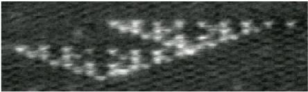
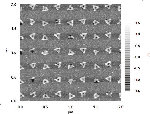
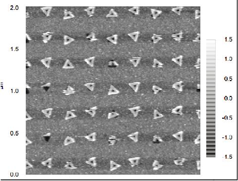
2 1 nanometer shapes with 2 pixel patterns, 6 nanometer resolution, 1 billion per drop, 9% yield (Rothemund) uses many distinct DNA strands, relatively expensive for higher complexity 1 nm Arbitrary shapes Arbitrary patterns on top of shapes 1 nm 2 nanometers 1 nanometers


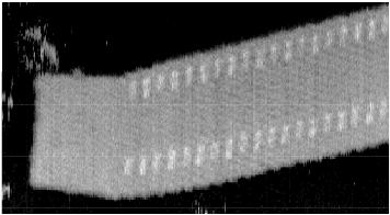
3 ATGGA GACCA ATGGA GACCA ATGGA CTGGT GACCA TACCT ATGGA GACCA CTGGT 42 nucleotides, 14.3 nm TACCT CTGGT TACCT ATGGA CTGGT GACCA TACCT CTGGT TACCT 6 tile wide DNA ribbon:
4
 but also work on metallization. DNA noncovalently wraps CNTs and allows them to disperse in buffer solution.")
5 Challenge 1: "Functionalization" electronically or optically active materials must be coupled to DNA nanostructures in high yield at specificed locations. We focus on carbon nanotubes (CNTs) but also work on metallization. DNA noncovalently wraps CNTs and allows them to disperse in buffer solution. An origami is made with 'red' and 'blue' DNA hooks, having different DNA sequences on top and bottom. Two batches of CNTs are made with complementary red or blue strands. Red and blue CNT assemble into crossbar FET on the origami. + + A device measurement is made Si/ SiO 2 Pd


6 To make nanostructures more rigid and to avoid aggregation origami-ribbon hybrids are used. red and blue hooks red tube blue tubes MOSFET geometry 5 nm crossbar Gate Channel


![CNT FET b V SD I SD a I SD [na] 4 3 2 I SD [na] 2 1 -- - -- V g =.](/docs-images/90/102850871/images/7-3.jpg "5V -- -- V g = -.5V ------ V g =.5V -.5..5 V SD [V] 1 V g I SD V SD =.")
7 Over 3% of tubes are within 1 degrees of the desired orientation Frequency Orientation of SWNT 22% 2% 76% Red side (-1) Unknown () Blue side (1) Angle Characterization of DNA self-assembled CNT FET b V SD I SD a I SD [na] I SD [na] V g =.5V V g = -.5V V g =.5V V SD [V] 1 V g I SD V SD =.85V V g [V]
8

9 Challenge 3, "Wiring-up" and "Bridging length scales": DNA nanostructures have a fundamental size mismatch with electronics at a larger spatial scale. E-beam patterning can only wire-up simple nanodevices. Still hard to build, we would like to self-assemble connections. E-beam cannot achieve wiring to complex objects at the nanoscale. Challenge 4, "Scaling-up": 2 pixels for DNA origami is a start, but we expect to want billions of devices. Similarly, a single FET is nice but we desire circuits. single origami max 2 devices VLSI chip
10
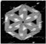
11 Rothemund's Aims: To continue work with IBM, to replicate positioning and orienting work at Caltech, so that CNT devices can be more easily characterized and integrated. origami shapes patterned DLC on Si placed shapes CNT organization To combine multiple origami to create large origami breadboards. A B C D jigsaw puzzle stacking bonds enable 8 pixels A B C D To create DNA structures with features that bridge the nano and microscales so that a complete device can be fabricated...
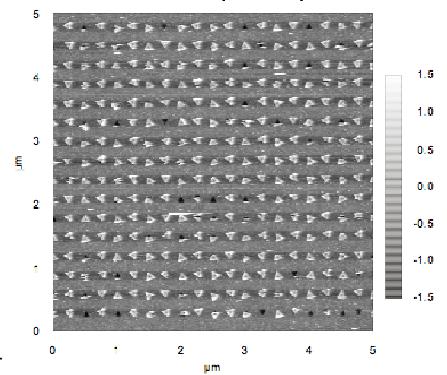
12 Bridging the nano and micro scales cross-shaped origami tiles further tile additions 5 x 2 microns 1 nm metallize strands with nanogold mineralize strands bearing peptides P N
13 Patterning of nanotubes (wires) so that they diverge and can be wired up at the microscale + = CNT FET + = (or colored tracks may be metallized)
14 Winfree's Aims: To use combined existing DNA self-assembly techniques (DNA origami, ribbons, algorithmic self-assembly, and periodic DNA crystals) to create squares of programmable size. These squares will have a pattern that is appropriate for a memory with demultiplexers, an architecture perfectly suited for useful circuits. To explore the addition of actual nanoelectronic components to the memory pattern, for example a crossbar lattice of carbon nanotubes. an origami seed n encoding the number n is added to a soup of tiles The 'computed' output is a square of size n tiles x n tiles with the origami embedded in one corner.

15 n n Self-assembly can compute: a simple example is counting. Counting tile set. 1 n n n 1 1 c c c c R 1 L S The pattern left behind is a template for a demultiplexer AND gate AND gate, lower input negated NOT gate Counting to a fixed length from an origami enables programmed growth of NxN squares A counter grown from origami Full N x N squares remain an important challenge. Error rates must be reduced. A termination scheme for counters must be demonstrated.
16 Input lines encode binary values for 6 (vertical) and 9 (horizontal) which are demultiplexed to access the red memory element. The light gray pattern underneath which determines the circuit would be created by the self-assembly of this 21 x 21 square.
17 Bockrath's Aims: To use short length-sorted carbon nanotubes to increase the yield of existing devices. (Many problems arise from very long tubes acting as bridges between multiple origami). To self-assemble and characterize circuits of more than one carbon-nanotube based device to create elementary logic gates and memory elements. To self-assemble novel devices to explore transport physics in nanostructures.
18 Rationally Engineered Logic gates and Memory Elements Utilizing Multiple Nanotubes Nanotube assembly Schematic circuit diagram Inverter V s V out V in SRAM V s V out NOR V s V s V out V in1 V in2
19 Novel Devices Probing Transport Physics in Nanostructures: Phase Coherence in Strongly-Interacting Electron Systems Many possibilities exist for making novel devices. DNA origami template for parallel nanotubes Tunable separation with desired values ~5-2 nm Interferometer device B V source drain I Nanotubes act as a which path? interferometer enabling the study of phase coherent transport in Nanotube-based Luttinger liquids via a transport experiment. The setup is analogous to a double slit experiment in optics. The magnetic field B tunes the phase by the Ahoronov-Bohm effect. Tubes must be closer together than the phase coherence length in the electrodes, which is readily obtainable using DNA based self-assembly.
20 Goddard's Aims: Electron transport in DNA-carbon nanotube hybrids: The effect of an insulating DNA layer between carbon nanotubes, silicon nanowires, and quantum dots is unknown. In some cases DNA may be removed from devices post-assembly, in other cases may remain. Thus it is important to simulate electron transport in carbon nanotube devices, with and without intervening DNA, starting with atomistic simulation (Next slide). Simulations of the placement process: The interactions which bind DNA structures to technological surfaces like silicon or diamond-like carbon are poorly understood. The best choice of experimental conditions, as well as the best choice of DNA shapes to bind can be explored by atomistic and mesoscale simulation. Free energies of correct and mismatched binding, and possible kinetic traps can be explored. patterned DLC on Si possible kinetic traps and mismatches
 -> quantum descriptions necessary. Theory and Modeling to Describe Quantum chemistry of molecule(s) + nanotube -> charge flow & bonding -> geometry & energy spectrum of the entire system.")
21 DNA-origami CNT-based Transistor V Junctions V I CNT DNA CNT µ 1 LUMO HOMO µ 2 E F Organic molecule Size of molecules << scattering lengths (e.g. mean free path, de Broglie wavelength, etc.) -> quantum descriptions necessary. Theory and Modeling to Describe Quantum chemistry of molecule(s) + nanotube -> charge flow & bonding -> geometry & energy spectrum of the entire system. Organo-metallic interface mechanics and transport. Need to treat molecule as finite and nanotubes as semi-infinite electrodes. Escape currents (through organic insulator layer). Conformation effects on electronic transport. Effect of finite bias. IV characteristic of self-assembled CNT-based transistor junctions.
 -4 4 Lower current,x 1asymmetric -3 I-V 1 transmission Ballistic transport theory (Landauer, Buttiker) 2e T (E,V )[ f1 (E! µ2 )! f2 (E!")
22 Multiscale Methodology: 1st-principles I-V validated by rotaxane modeling Density-functional theory (Hohenberg-Kohn-Sham) ( #1,2 = i "1,2! " ( + 1,2 ) T (E,V ) = Tr!1G! 2G + self-energy contact widening ) -4 4 Lower current,x 1asymmetric -3 I-V 1 transmission Ballistic transport theory (Landauer, Buttiker) 2e T (E,V )[ f1 (E! µ2 )! f2 (E! µ1 )] de current #!" h T(E,V) 2 di 2e G=! T conductance dv h " e.g. Rotaxane switch 6 di/dv di/dv vs. junction bias and gate bias S S O O +N O O O N+ S S S S O O O +N O O O N+ -9 source to drai n volta ge (mv ) x1 I= gate volta ge 2.55V na -9 Gm = (Em Sm! H m! "1! " 2 )!1 2 Γ1 x1 Green s ftn. Formalism (Fisher-Lee) m 1 gate voltage (V) µ1 " µ1 = ev, n! H electro-chemical potential na Molecular Mechanics Dynamics d2r geometry F=m 2 dt

 =!")
 de molecule")
23 Further validation: bi-phenyl-dithiol modeling T(E) contact 2e µ 2 I V ) =! T ( E, V )( f1 " f h µ 1 ( 2 ) de molecule I(V) contact Au (111)
24 Relevance to the Office of Naval Research Fundamental advances in microelectronics underlie all of our country's defense systems, from networked warfare to avionic systems. Eventually, self-assembly based methods may be the only path forward to more powerful nanoelectronic systems. DNA self-assembly uses non-hazardous "green" chemistries, decreasing the Navy's environmental footprint. DNA self-assembly techniques may yield lower cost electronics "grown" from cheap components without capital investment in conventional chip fabs.
25 Budget for 4 years, $2.6 million including: PI: Paul Rothemund: $2K/yr for Senior Research Associate salary and materials Co-PI: Mark Bockrath $1K/yr for 1 graduate student and materials Co-PI: Bill Goddard $1K/yr for 1 graduate student and materials Co-PI: Erik Winfree $1K/yr for 1 graduate student and materials Equipment $15K/yr including plasma etcher/cleaner ($2K), wafer-scale Atomic Force Microscope ($2K) temperature-controlled dynamic light scattering ($5K).
Nanoelectronics. Topics
 Nanoelectronics Topics Moore s Law Inorganic nanoelectronic devices Resonant tunneling Quantum dots Single electron transistors Motivation for molecular electronics The review article Overview of Nanoelectronic
CSCI 2570 Introduction to Nanocomputing
 CSCI 2570 Introduction to Nanocomputing The Emergence of Nanotechnology John E Savage Purpose of the Course The end of Moore s Law is in sight. Researchers are now exploring replacements for standard methods
EN2912C: Future Directions in Computing Lecture 08: Overview of Near-Term Emerging Computing Technologies
 EN2912C: Future Directions in Computing Lecture 08: Overview of Near-Term Emerging Computing Technologies Prof. Sherief Reda Division of Engineering Brown University Fall 2008 1 Near-term emerging computing
There's Plenty of Room at the Bottom
 There's Plenty of Room at the Bottom 12/29/1959 Feynman asked why not put the entire Encyclopedia Britannica (24 volumes) on a pin head (requires atomic scale recording). He proposed to use electron microscope
During such a time interval, the MOS is said to be in "deep depletion" and the only charge present in the semiconductor is the depletion charge.
 Q1 (a) If we apply a positive (negative) voltage step to a p-type (n-type) MOS capacitor, which is sufficient to generate an inversion layer at equilibrium, there is a time interval, after the step, when
single-electron electron tunneling (SET)
") single-electron electron tunneling (SET) classical dots (SET islands): level spacing is NOT important; only the charging energy (=classical effect, many electrons on the island) quantum dots: : level spacing
single-electron electron tunneling (SET) classical dots (SET islands): level spacing is NOT important; only the charging energy (=classical effect, many electrons on the island) quantum dots: : level spacing
Ultralow-Power Reconfigurable Computing with Complementary Nano-Electromechanical Carbon Nanotube Switches
 Ultralow-Power Reconfigurable Computing with Complementary Nano-Electromechanical Carbon Nanotube Switches Presenter: Tulika Mitra Swarup Bhunia, Massood Tabib-Azar, and Daniel Saab Electrical Eng. And
Photoresponsive Nanoscale Columnar Transistors
 Photoresponsive Nanoscale Columnar Transistors Xuefeng Guo, Shengxiong Xiao, Matthew Myers, Qian Miao, Michael L. Steigerwald, and Colin Nuckolls. Center for Nanochemistry, Beijing National Laboratory
Gold Nanoparticles Floating Gate MISFET for Non-Volatile Memory Applications
 Gold Nanoparticles Floating Gate MISFET for Non-Volatile Memory Applications D. Tsoukalas, S. Kolliopoulou, P. Dimitrakis, P. Normand Institute of Microelectronics, NCSR Demokritos, Athens, Greece S. Paul,
RAJASTHAN TECHNICAL UNIVERSITY, KOTA
 RAJASTHAN TECHNICAL UNIVERSITY, KOTA (Electronics & Communication) Submitted By: LAKSHIKA SOMANI E&C II yr, IV sem. Session: 2007-08 Department of Electronics & Communication Geetanjali Institute of Technical
3-month progress Report
 3-month progress Report Graphene Devices and Circuits Supervisor Dr. P.A Childs Table of Content Abstract... 1 1. Introduction... 1 1.1 Graphene gold rush... 1 1.2 Properties of graphene... 3 1.3 Semiconductor
GRAPHENE NANORIBBONS Nahid Shayesteh,
 USC Department of Physics Graduate Seminar 1 GRAPHENE NANORIBBONS Nahid Shayesteh, Outlines 2 Carbon based material Discovery and innovation of graphen Graphene nanoribbons structure Application of Graphene
Molecular Self-Assembly: Models and Algorithms
 Molecular Self-Assembly: Models and Algorithms Ashish Goel Stanford University MS&E 319/CS 369X; Research topics in optimization; Stanford University, Spring 2003-04 http://www.stanford.edu/~ashishg Self-Assembly
Interdisciplinary Nanoscience Center University of Aarhus, Denmark. Design and Imaging. Assistant Professor.
 Interdisciplinary Nanoscience Center University of Aarhus, Denmark Design and Imaging DNA Nanostructures Assistant Professor Wael Mamdouh wael@inano.dk Molecular Self-assembly Synthesis, SPM microscopy,
materials, devices and systems through manipulation of matter at nanometer scale and exploitation of novel phenomena which arise because of the
 Nanotechnology is the creation of USEFUL/FUNCTIONAL materials, devices and systems through manipulation of matter at nanometer scale and exploitation of novel phenomena which arise because of the nanometer
Emerging Research Devices: A Study of CNTFET and SET as a replacement for SiMOSFET
 1 Emerging Research Devices: A Study of CNTFET and SET as a replacement for SiMOSFET Mahmoud Lababidi, Krishna Natarajan, Guangyu Sun Abstract Since the development of the Silicon MOSFET, it has been the
Carbon based Nanoscale Electronics
 Carbon based Nanoscale Electronics 09 02 200802 2008 ME class Outline driving force for the carbon nanomaterial electronic properties of fullerene exploration of electronic carbon nanotube gold rush of
are microscopically large but macroscopically small contacts which may be connected to a battery to provide the bias voltage across the junction.
 At present, we observe a long-lasting process of miniaturization of electronic devices. The ultimate limit for the miniaturization of electronic components is set by the atomic scale. However, in the case
Nanotechnology where size matters
 Nanotechnology where size matters J Emyr Macdonald Overview Ways of seeing very small things What is nanotechnology and why is it important? Building nanostructures What we can do with nanotechnology?
DocumentToPDF trial version, to remove this mark, please register this software.
 PAPER PRESENTATION ON Carbon Nanotube - Based Nonvolatile Random Access Memory AUTHORS M SIVARAM PRASAD Sivaram.443@gmail.com B N V PAVAN KUMAR pavankumar.bnv@gmail.com 1 Carbon Nanotube- Based Nonvolatile
From nanophysics research labs to cell phones. Dr. András Halbritter Department of Physics associate professor
 From nanophysics research labs to cell phones Dr. András Halbritter Department of Physics associate professor Curriculum Vitae Birth: 1976. High-school graduation: 1994. Master degree: 1999. PhD: 2003.
Lecture 0: Introduction
 Lecture 0: Introduction Introduction q Integrated circuits: many transistors on one chip q Very Large Scale Integration (VLSI): bucketloads! q Complementary Metal Oxide Semiconductor Fast, cheap, low power
Computers of the Future? Moore s Law Ending in 2018?
 Computers of the Future? CS 221 Moore s Law Ending in 2018? Moore s Law: Processor speed / number transistors doubling approximately 18 months 1 Moore s Law Moore s Law Recent research predicts an end
Computational Modeling of Molecular Electronics. Chao-Cheng Kaun
 Computational Modeling of Molecular Electronics Chao-Cheng Kaun Research Center for Applied Sciences, Academia Sinica Department of Physics, National Tsing Hua University May 9, 2007 Outline: 1. Introduction
Nanoparticle Devices. S. A. Campbell, ECE C. B. Carter, CEMS H. Jacobs, ECE J. Kakalios, Phys. U. Kortshagen, ME. Institute of Technology
 Nanoparticle Devices S. A. Campbell, ECE C. B. Carter, CEMS H. Jacobs, ECE J. Kakalios, Phys. U. Kortshagen, ME Applications of nanoparticles Flash Memory Tiwari et al., Appl. Phys. Lett. 68, 1377, 1996.
Exceptional ballistic transport in epigraphene. Walt de Heer Georgia Institute of Technology
 Exceptional ballistic transport in epigraphene Walt de Heer Georgia Institute of Technology Program Objective First formulated in 2001 and patented in 2003, our objective is to develop nanoelectronics
Hrudya Nair. COBDEN RESEARCH GROUP Nanodevice Physics Lab CAPACITOR BRIDGE
 Hrudya Nair COBDEN RESEARCH GROUP Nanodevice Physics Lab CAPACITOR BRIDGE Overview: In this lab students will learn to measure the capacitance of an unknown capacitor by building a capacitor bridge circuit
CHAPTER 11 Semiconductor Theory and Devices
 CHAPTER 11 Semiconductor Theory and Devices 11.1 Band Theory of Solids 11.2 Semiconductor Theory 11.3 Semiconductor Devices 11.4 Nanotechnology It is evident that many years of research by a great many
The Nanotube SQUID. uhu,, M. Monthioux,, V. Bouchiat, W. Wernsdorfer, CEMES-Toulouse, CRTBT & LLN Grenoble
 The Nanotube SQUID J.-P. Cleuziou,, Th. Ondarçuhu uhu,, M. Monthioux,, V. Bouchiat, W. Wernsdorfer, CEMES-Toulouse, CRTBT & LLN Grenoble Outline Sample fabrication Proximity effect in CNT The CNT superconducting
Semi-Conductors insulators semi-conductors N-type Semi-Conductors P-type Semi-Conductors
 Semi-Conductors In the metal materials considered earlier, the coupling of the atoms together to form the material decouples an electron from each atom setting it free to roam around inside the material.
Introduction to Nanotechnology Chapter 5 Carbon Nanostructures Lecture 1
 Introduction to Nanotechnology Chapter 5 Carbon Nanostructures Lecture 1 ChiiDong Chen Institute of Physics, Academia Sinica chiidong@phys.sinica.edu.tw 02 27896766 Carbon contains 6 electrons: (1s) 2,
Nanostrukturphysik (Nanostructure Physics)
") Nanostrukturphysik (Nanostructure Physics) Prof. Yong Lei & Dr. Yang Xu Fachgebiet 3D-Nanostrukturierung, Institut für Physik Contact: yong.lei@tu-ilmenau.de; yang.xu@tu-ilmenau.de Office: Unterpoerlitzer
Nanostrukturphysik (Nanostructure Physics) Prof. Yong Lei & Dr. Yang Xu Fachgebiet 3D-Nanostrukturierung, Institut für Physik Contact: yong.lei@tu-ilmenau.de; yang.xu@tu-ilmenau.de Office: Unterpoerlitzer
Single Electron Transistor (SET)
") Single Electron Transistor (SET) SET: e - e - dot A single electron transistor is similar to a normal transistor (below), except 1) the channel is replaced by a small dot. C g 2) the dot is separated from
Single Electron Transistor (SET) SET: e - e - dot A single electron transistor is similar to a normal transistor (below), except 1) the channel is replaced by a small dot. C g 2) the dot is separated from
EV Group. Engineered Substrates for future compound semiconductor devices
 EV Group Engineered Substrates for future compound semiconductor devices Engineered Substrates HB-LED: Engineered growth substrates GaN / GaP layer transfer Mobility enhancement solutions: III-Vs to silicon
3/10/2013. Lecture #1. How small is Nano? (A movie) What is Nanotechnology? What is Nanoelectronics? What are Emerging Devices?
 What is Nanotechnology? What is Nanoelectronics? What are Emerging Devices?") EECS 498/598: Nanocircuits and Nanoarchitectures Lecture 1: Introduction to Nanotelectronic Devices (Sept. 5) Lectures 2: ITRS Nanoelectronics Road Map (Sept 7) Lecture 3: Nanodevices; Guest Lecture by
EECS 498/598: Nanocircuits and Nanoarchitectures Lecture 1: Introduction to Nanotelectronic Devices (Sept. 5) Lectures 2: ITRS Nanoelectronics Road Map (Sept 7) Lecture 3: Nanodevices; Guest Lecture by
How a single defect can affect silicon nano-devices. Ted Thorbeck
 How a single defect can affect silicon nano-devices Ted Thorbeck tedt@nist.gov The Big Idea As MOS-FETs continue to shrink, single atomic scale defects are beginning to affect device performance Gate Source
Administrative Stuff
 EE141- Spring 2004 Digital Integrated Circuits Lecture 30 PERSPECTIVES 1 Administrative Stuff Homework 10 posted just for practice. No need to turn in (hw 9 due today). Normal office hours next week. HKN
Graphene and Carbon Nanotubes
 Graphene and Carbon Nanotubes 1 atom thick films of graphite atomic chicken wire Novoselov et al - Science 306, 666 (004) 100μm Geim s group at Manchester Novoselov et al - Nature 438, 197 (005) Kim-Stormer
Supplementary Figure 1: Micromechanical cleavage of graphene on oxygen plasma treated Si/SiO2. Supplementary Figure 2: Comparison of hbn yield.
 1 2 3 4 Supplementary Figure 1: Micromechanical cleavage of graphene on oxygen plasma treated Si/SiO 2. Optical microscopy images of three examples of large single layer graphene flakes cleaved on a single
DESIGN OF QCA FULL ADDER CIRCUIT USING CORNER APPROACH INVERTER
 Research Manuscript Title DESIGN OF QCA FULL ADDER CIRCUIT USING CORNER APPROACH INVERTER R.Rathi Devi 1, PG student/ece Department, Vivekanandha College of Engineering for Women rathidevi24@gmail.com
Monolayer Semiconductors
 Monolayer Semiconductors Gilbert Arias California State University San Bernardino University of Washington INT REU, 2013 Advisor: Xiaodong Xu (Dated: August 24, 2013) Abstract Silicon may be unable to
Digital Electronics Part II - Circuits
 Digital Electronics Part - Circuits Dr.. J. Wassell Gates from Transistors ntroduction Logic circuits are non-linear, consequently we will introduce a graphical technique for analysing such circuits The
Available online at ScienceDirect. Procedia Materials Science 11 (2015 )
") Available online at www.sciencedirect.com ScienceDirect Procedia Materials Science 11 (2015 ) 287 292 5th International Biennial Conference on Ultrafine Grained and Nanostructured Materials, UFGNSM15 Tunneling
Available online at www.sciencedirect.com ScienceDirect Procedia Materials Science 11 (2015 ) 287 292 5th International Biennial Conference on Ultrafine Grained and Nanostructured Materials, UFGNSM15 Tunneling
Carbon Nanotube Electronics
 Carbon Nanotube Electronics Jeorg Appenzeller, Phaedon Avouris, Vincent Derycke, Stefan Heinz, Richard Martel, Marko Radosavljevic, Jerry Tersoff, Shalom Wind H.-S. Philip Wong hspwong@us.ibm.com IBM T.J.
Chapter 5 Nanomanipulation. Chapter 5 Nanomanipulation. 5.1: With a nanotube. Cutting a nanotube. Moving a nanotube
 Objective: learn about nano-manipulation techniques with a STM or an AFM. 5.1: With a nanotube Moving a nanotube Cutting a nanotube Images at large distance At small distance : push the NT Voltage pulse
Diameter Optimization for Highest Degree of Ballisticity of Carbon Nanotube Field Effect Transistors I. Khan, O. Morshed and S. M.
 Diameter Optimization for Highest Degree of Ballisticity of Carbon Nanotube Field Effect Transistors I. Khan, O. Morshed and S. M. Mominuzzaman Department of Electrical and Electronic Engineering, Bangladesh
PHYS 3313 Section 001 Lecture #21 Monday, Nov. 26, 2012
 PHYS 3313 Section 001 Lecture #21 Monday, Nov. 26, 2012 Superconductivity Theory, The Cooper Pair Application of Superconductivity Semi-Conductor Nano-technology Graphene 1 Announcements Your presentations
Electronic transport in low dimensional systems
 Electronic transport in low dimensional systems For example: 2D system l
Analytical Modeling of Threshold Voltage for a. Biaxial Strained-Si-MOSFET
 Contemporary Engineering Sciences, Vol. 4, 2011, no. 6, 249 258 Analytical Modeling of Threshold Voltage for a Biaxial Strained-Si-MOSFET Amit Chaudhry Faculty of University Institute of Engineering and
Trends in Nanotechnology: Self-Assembly and Defect Tolerance
 Trends in Nanotechnology: Self-Assembly and Defect Tolerance (Invited paper submitted to MSTNEWS 3 January 2001) T. I. Kamins and R. Stanley Williams Quantum Science Research, Hewlett-Packard Laboratories,
29: Nanotechnology. What is Nanotechnology? Properties Control and Understanding. Nanomaterials
 29: Nanotechnology What is Nanotechnology? Properties Control and Understanding Nanomaterials Making nanomaterials Seeing at the nanoscale Quantum Dots Carbon Nanotubes Biology at the Nanoscale Some Applications
Formation mechanism and Coulomb blockade effect in self-assembled gold quantum dots
 Formation mechanism and Coulomb blockade effect in self-assembled gold quantum dots S. F. Hu a) National Nano Device Laboratories, Hsinchu 300, Taiwan R. L. Yeh and R. S. Liu Department of Chemistry, National
Impact of disorder and topology in two dimensional systems at low carrier densities
 Impact of disorder and topology in two dimensional systems at low carrier densities A Thesis Submitted For the Degree of Doctor of Philosophy in the Faculty of Science by Mohammed Ali Aamir Department
Electrical and Optical Properties. H.Hofmann
 Introduction to Nanomaterials Electrical and Optical Properties H.Hofmann Electrical Properties Ohm: G= σw/l where is the length of the conductor, measured in meters [m], A is the cross-section area of
First-Principles Modeling of Charge Transport in Molecular Junctions
 First-Principles Modeling of Charge Transport in Molecular Junctions Chao-Cheng Kaun Research Center for Applied Sciences, Academia Sinica Department of Physics, National Tsing Hua University September
Surface plasmon waveguides
 Surface plasmon waveguides Introduction Size Mismatch between Scaled CMOS Electronics and Planar Photonics Photonic integrated system with subwavelength scale components CMOS transistor: Medium-sized molecule
OMEN an atomistic and full-band quantum transport simulator for post-cmos nanodevices
 Purdue University Purdue e-pubs Other Nanotechnology Publications Birck Nanotechnology Center 8-18-28 OMEN an atomistic and full-band quantum transport simulator for post-cmos nanodevices Mathieu Luisier
ELECTRONIC DEVICES AND CIRCUITS SUMMARY
 ELECTRONIC DEVICES AND CIRCUITS SUMMARY Classification of Materials: Insulator: An insulator is a material that offers a very low level (or negligible) of conductivity when voltage is applied. Eg: Paper,
Nanotechnology. Yung Liou P601 Institute of Physics Academia Sinica
 Nanotechnology Yung Liou P601 yung@phys.sinica.edu.tw Institute of Physics Academia Sinica 1 1st week Definition of Nanotechnology The Interagency Subcommittee on Nanoscale Science, Engineering and Technology
Nanoscale Heat Transfer and Information Technology
 Response to K.E. Goodson Nanoscale Heat Transfer and Information Technology Gang Chen Mechanical Engineering Department Massachusetts Institute of Technology Cambridge, MA 02139 Rohsenow Symposium on Future
Indium arsenide quantum wire trigate metal oxide semiconductor field effect transistor
 JOURNAL OF APPLIED PHYSICS 99, 054503 2006 Indium arsenide quantum wire trigate metal oxide semiconductor field effect transistor M. J. Gilbert a and D. K. Ferry Department of Electrical Engineering and
A final review session will be offered on Thursday, May 10 from 10AM to 12noon in 521 Cory (the Hogan Room).
.") A final review session will be offered on Thursday, May 10 from 10AM to 12noon in 521 Cory (the Hogan Room). The Final Exam will take place from 12:30PM to 3:30PM on Saturday May 12 in 60 Evans.» All of
A final review session will be offered on Thursday, May 10 from 10AM to 12noon in 521 Cory (the Hogan Room). The Final Exam will take place from 12:30PM to 3:30PM on Saturday May 12 in 60 Evans.» All of
ELEN0037 Microelectronic IC Design. Prof. Dr. Michael Kraft
 ELEN0037 Microelectronic IC Design Prof. Dr. Michael Kraft Lecture 2: Technological Aspects Technology Passive components Active components CMOS Process Basic Layout Scaling CMOS Technology Integrated
L ECE 4211 UConn F. Jain Scaling Laws for NanoFETs Chapter 10 Logic Gate Scaling
 L13 04202017 ECE 4211 UConn F. Jain Scaling Laws for NanoFETs Chapter 10 Logic Gate Scaling Scaling laws: Generalized scaling (GS) p. 610 Design steps p.613 Nanotransistor issues (page 626) Degradation
Black phosphorus: A new bandgap tuning knob
 Black phosphorus: A new bandgap tuning knob Rafael Roldán and Andres Castellanos-Gomez Modern electronics rely on devices whose functionality can be adjusted by the end-user with an external knob. A new
Transport through Andreev Bound States in a Superconductor-Quantum Dot-Graphene System
 Transport through Andreev Bound States in a Superconductor-Quantum Dot-Graphene System Nadya Mason Travis Dirk, Yung-Fu Chen, Cesar Chialvo Taylor Hughes, Siddhartha Lal, Bruno Uchoa Paul Goldbart University
Lecture 3: Heterostructures, Quasielectric Fields, and Quantum Structures
 Lecture 3: Heterostructures, Quasielectric Fields, and Quantum Structures MSE 6001, Semiconductor Materials Lectures Fall 2006 3 Semiconductor Heterostructures A semiconductor crystal made out of more
Nanotechnology Nanofabrication of Functional Materials. Marin Alexe Max Planck Institute of Microstructure Physics, Halle - Germany
 Nanotechnology Nanofabrication of Functional Materials Marin Alexe Max Planck Institute of Microstructure Physics, Halle - Germany Contents Part I History and background to nanotechnology Nanoworld Nanoelectronics
6545(Print), ISSN (Online) Volume 4, Issue 3, May - June (2013), IAEME & TECHNOLOGY (IJEET)
, ISSN (Online) Volume 4, Issue 3, May - June (2013), IAEME & TECHNOLOGY (IJEET)") INTERNATIONAL International Journal of JOURNAL Electrical Engineering OF ELECTRICAL and Technology (IJEET), ENGINEERING ISSN 0976 & TECHNOLOGY (IJEET) ISSN 0976 6545(Print) ISSN 0976 6553(Online) Volume
INTERNATIONAL International Journal of JOURNAL Electrical Engineering OF ELECTRICAL and Technology (IJEET), ENGINEERING ISSN 0976 & TECHNOLOGY (IJEET) ISSN 0976 6545(Print) ISSN 0976 6553(Online) Volume
Simple piezoresistive accelerometer
 Simple piezoresistive pressure sensor Simple piezoresistive accelerometer Simple capacitive accelerometer Cap wafer C(x)=C(x(a)) Cap wafer may be micromachined silicon, pyrex, Serves as over-range protection,
Formation of unintentional dots in small Si nanostructures
 Superlattices and Microstructures, Vol. 28, No. 5/6, 2000 doi:10.1006/spmi.2000.0942 Available online at http://www.idealibrary.com on Formation of unintentional dots in small Si nanostructures L. P. ROKHINSON,
Introduction to CMOS VLSI Design Lecture 1: Introduction
 Introduction to CMOS VLSI Design Lecture 1: Introduction David Harris, Harvey Mudd College Kartik Mohanram and Steven Levitan University of Pittsburgh Introduction Integrated circuits: many transistors
Self-study problems and questions Processing and Device Technology, FFF110/FYSD13
 Self-study problems and questions Processing and Device Technology, FFF110/FYSD13 Version 2016_01 In addition to the problems discussed at the seminars and at the lectures, you can use this set of problems
Chapter 12 - Modern Materials
 Chapter 12 - Modern Materials 12.1 Semiconductors Inorganic compounds that semiconduct tend to have chemical formulas related to Si and Ge valence electron count of four. Semiconductor conductivity can
EE 330 Lecture 3. Basic Concepts. Feature Sizes, Manufacturing Costs, and Yield
 EE 330 Lecture 3 Basic Concepts Feature Sizes, Manufacturing Costs, and Yield Review from Last Time Analog Flow VLSI Design Flow Summary System Description Circuit Design (Schematic) SPICE Simulation Simulation
Electronic structure and transport in silicon nanostructures with non-ideal bonding environments
 Purdue University Purdue e-pubs Other Nanotechnology Publications Birck Nanotechnology Center 9-15-2008 Electronic structure and transport in silicon nanostructures with non-ideal bonding environments
Thin Film Transistors (TFT)
") Thin Film Transistors (TFT) a-si TFT - α-si:h (Hydrogenated amorphous Si) deposited with a PECVD system (low temp. process) replaces the single crystal Si substrate. - Inverted staggered structure with
Thin Film Transistors (TFT) a-si TFT - α-si:h (Hydrogenated amorphous Si) deposited with a PECVD system (low temp. process) replaces the single crystal Si substrate. - Inverted staggered structure with
Evaluation of Electronic Characteristics of Double Gate Graphene Nanoribbon Field Effect Transistor for Wide Range of Temperatures
 Evaluation of Electronic Characteristics of Double Gate Graphene Nanoribbon Field Effect Transistor for Wide Range of Temperatures 1 Milad Abtin, 2 Ali Naderi 1 Department of electrical engineering, Masjed
NANOELECTRONICS beyond CMOS
 NANOELECTRONICS beyond CMOS David Pulfrey 1 NNI definition of Nanotechnology 1-10 nm is better But Intel prefer... 2 Bourianoff04 1 3 Bourianoff04 4 Moravec04 2 Increasing the Integration Level functional
Advanced Topics In Solid State Devices EE290B. Will a New Milli-Volt Switch Replace the Transistor for Digital Applications?
 Advanced Topics In Solid State Devices EE290B Will a New Milli-Volt Switch Replace the Transistor for Digital Applications? August 28, 2007 Prof. Eli Yablonovitch Electrical Engineering & Computer Sciences
ESE370: Circuit-Level Modeling, Design, and Optimization for Digital Systems
 ESE370: Circuit-Level Modeling, Design, and Optimization for Digital Systems Lec 6: September 14, 2015 MOS Model You are Here: Transistor Edition! Previously: simple models (0 and 1 st order) " Comfortable
ᣂቇⴚ㗔 䇸䉮䊮䊏䊠䊷䊁䉞䉪䉴䈮䉋䉎 䊂䉱䉟䊮䋺ⶄว 㑐䈫㕖ᐔⴧ䉻䉟䊅䊚䉪䉴䇹 ᐔᚑ22ᐕᐲ ળ䇮2011ᐕ3 4ᣣ䇮 ੩ᄢቇᧄㇹ䉨䊞䊮䊌䉴 㗄 A02 ኒᐲ 㑐ᢙᴺℂ 䈮ၮ䈨䈒㕖ᐔⴧ 䊅䊉䉴䉬䊷䊦㔚 વዉ䉻䉟䊅䊚䉪䉴 ઍ ᄢᎿ ㆺ
 22201134 A02 GCOE Si device (further downsizing) Novel nanostructures (such as atomic chain) Nanoscale multi-terminal resistance measurement Carbon nanotube transistor Atomic switch Interplay:l Dynamics:
CONDUCTANCE STATES OF MOLECULAR JUNCTIONS FOR ENCODING BINARY INFORMATION: A COMPUTATIONAL APPROACH. A Dissertation LUIS ALBERTO AGAPITO
 CONDUCTANCE STATES OF MOLECULAR JUNCTIONS FOR ENCODING BINARY INFORMATION: A COMPUTATIONAL APPROACH A Dissertation by LUIS ALBERTO AGAPITO Submitted to the Office of Graduate Studies of Texas A&M University
Nanotechnology? Source: National Science Foundation (NSF), USA
, USA") 2 2 Nanotechnology? Ability to work at the atomic, molecular and even sub-molecular levels in order to create and use material structures, devices and systems with new properties and functions Source:
2 2 Nanotechnology? Ability to work at the atomic, molecular and even sub-molecular levels in order to create and use material structures, devices and systems with new properties and functions Source:
QUANTUM INTERFERENCE IN SEMICONDUCTOR RINGS
 QUANTUM INTERFERENCE IN SEMICONDUCTOR RINGS PhD theses Orsolya Kálmán Supervisors: Dr. Mihály Benedict Dr. Péter Földi University of Szeged Faculty of Science and Informatics Doctoral School in Physics
There s plenty of room at the bottom! - R.P. Feynman, Nanostructure: a piece of material with at least one dimension less than 100 nm in extent.
 Nanostructures and Nanotechnology There s plenty of room at the bottom! - R.P. Feynman, 1959 Materials behave differently when structured at the nm scale than they do in bulk. Technologies now exist that
OPTI510R: Photonics. Khanh Kieu College of Optical Sciences, University of Arizona Meinel building R.626
 OPTI510R: Photonics Khanh Kieu College of Optical Sciences, University of Arizona kkieu@optics.arizona.edu Meinel building R.626 Announcements HW#3 is assigned due Feb. 20 st Mid-term exam Feb 27, 2PM
wire z axis Under these assumptions, if we model the electrons by plane waves in the z direction we get n E, n, 1,2,
 Part 4. Two Terminal Quantum Wire Devices Part 4. Two Terminal Quantum Wire Devices Let s consider a quantum wire between two contacts. As we saw in Part, a quantum wire is a one-dimensional conductor.
Semiconductor Nanowires: Motivation
 Semiconductor Nanowires: Motivation Patterning into sub 50 nm range is difficult with optical lithography. Self-organized growth of nanowires enables 2D confinement of carriers with large splitting of
Moore s Law Forever?
 NCN Nanotechnology 101 Series Moore s Law Forever? Mark Lundstrom Purdue University Network for Computational Nanotechnology West Lafayette, IN USA NCN 1) Background 2) Transistors 3) CMOS 4) Beyond CMOS
Lecture 1: Circuits & Layout
 Lecture 1: Circuits & Layout Outline q A Brief History q CMOS Gate esign q Pass Transistors q CMOS Latches & Flip-Flops q Standard Cell Layouts q Stick iagrams 2 A Brief History q 1958: First integrated
Supplementary Methods A. Sample fabrication
 Supplementary Methods A. Sample fabrication Supplementary Figure 1(a) shows the SEM photograph of a typical sample, with three suspended graphene resonators in an array. The cross-section schematic is
Fabrication Methods: Chapter 4. Often two methods are typical. Top Down Bottom up. Begins with atoms or molecules. Begins with bulk materials
 Fabrication Methods: Chapter 4 Often two methods are typical Top Down Bottom up Begins with bulk materials Begins with atoms or molecules Reduced in size to nano By thermal, physical Chemical, electrochemical
Nanoimprint Lithography
 Nanoimprint Lithography Wei Wu Quantum Science Research Advanced Studies HP Labs, Hewlett-Packard Email: wei.wu@hp.com Outline Background Nanoimprint lithography Thermal based UV-based Applications based
Available online at ScienceDirect. Procedia Materials Science 11 (2015 )
") Available online at www.sciencedirect.com ScienceDirect Procedia Materials Science 11 (2015 ) 407 411 5th International Biennial Conference on Ultrafine Grained and Nanostructured Materials, FGNSM15 Simulation
Available online at www.sciencedirect.com ScienceDirect Procedia Materials Science 11 (2015 ) 407 411 5th International Biennial Conference on Ultrafine Grained and Nanostructured Materials, FGNSM15 Simulation
EE410 vs. Advanced CMOS Structures
 EE410 vs. Advanced CMOS Structures Prof. Krishna S Department of Electrical Engineering S 1 EE410 CMOS Structure P + poly-si N + poly-si Al/Si alloy LPCVD PSG P + P + N + N + PMOS N-substrate NMOS P-well
Multiple Gate CMOS and Beyond
 Multiple CMOS and Beyond Dept. of EECS, KAIST Yang-Kyu Choi Outline 1. Ultimate Scaling of MOSFETs - 3nm Nanowire FET - 8nm Non-Volatile Memory Device 2. Multiple Functions of MOSFETs 3. Summary 2 CMOS
Supporting Information
 Supporting Information Monolithically Integrated Flexible Black Phosphorus Complementary Inverter Circuits Yuanda Liu, and Kah-Wee Ang* Department of Electrical and Computer Engineering National University
Supporting Online Material for
 www.sciencemag.org/cgi/content/full/327/5966/662/dc Supporting Online Material for 00-GHz Transistors from Wafer-Scale Epitaxial Graphene Y.-M. Lin,* C. Dimitrakopoulos, K. A. Jenkins, D. B. Farmer, H.-Y.
Nanoparticles, nanorods, nanowires
 Nanoparticles, nanorods, nanowires Nanoparticles, nanocrystals, nanospheres, quantum dots, etc. Drugs, proteins, etc. Nanorods, nanowires. Optical and electronic properties. Organization using biomolecules.