Nanoelectronics. Topics
|
|
|
- Lesley Hunt
- 5 years ago
- Views:
Transcription
1 Nanoelectronics Topics Moore s Law Inorganic nanoelectronic devices Resonant tunneling Quantum dots Single electron transistors Motivation for molecular electronics The review article Overview of Nanoelectronic Devices by David Goldhaber- Gordon et al. is available on the course website.
2 1,000, ,000 10,000 1, K Moore s Law 1 Billion Transistors Pentium III Processor Pentium II Processor Pentium Pro Processor Pentium Processor i486 Processor i386 Processor The Number of of Transistors Per Chip Will Double Every Months Source: Intel
3 Benefits of scaling Reducing the size of the transistors makes them faster and keeps the power consumption reasonable. Putting more transistors in a circuit enables more computation. Integrating several chips into one improves reliability. Cost per transistor goes down.
4 How long will Moore s Law continue? Billions of dollars will be spent to make sure that improvement of silicon chips stay on the curve predicted by Moore, but there are some serious obstacles that must be overcome.
 p.")
5 Expected obstacles With very small channels, carriers could tunnel all the way across, even when there isn t supposed to be any current. Paul Packan, Science 285 (1999) p

6 Interconnects 0.13µm Cu Interconnects The speed of circuits is starting to be limited by the RC time constant of the interconnects rather than the switching speed of the transistors. R is being reduced by using Cu instead of Al. C is being reduced by using a low-k dielectric, such as nanoporous silica, to insulate the wires from each other. From Craig Barrett (Intel)
7 Other obstacles The resolution of lithography must go below 100 nm. Heat must be dissipated. Fabrication plants are costing billions of dollars. As daunting as the problems are, my bet is that the silicon industry will find ways to solve them for at least 7 more years and maybe much longer. The focus of this course is not how to push silicon (or germanium) technology forward, but how to make new devices with non-traditional fabrication techniques. We will look at candidates for post 2010 circuits.

8 Nanoelectronics Smaller devices will be made for all the reasons just given. When the devices become smaller than 100 nm in size, quantum mechanical effects such as energy quantization and tunneling will become important. These effects could be a problem, but they could be turned into an advantage.

9 Confinement quantizes the energy levels If V O = infinite, then E k = 2π = = λ nπ L h k h π n = 2 2m 2mL 2 For small L, the spacing between energy levels is larger. Coldren, Corzine, Diode Lasers, 1995.
10 Quantum wells (Electrons confined in one-dimension) Energy AlGaAs GaAs AlGaAs Distance Electrons are confined in one dimension and free in the other. A common method for making quantum wells is to use epitaxial methods to deposit alloys with varying composition onto a substrate.

11 Quantum dots (artificial atoms) Electrons are confined in all three dimensions. The energy levels are discreet, so these quantum dots are much like atoms. Review Article A.P. Alivisatos, Semiconductor Clusters, Nanocrystals, and Quantum Dots, Science 271 (1996) p. 933.
 8706.")

12 M.G. Bawendi et al. JACS 115 (1993) Nanocrystals The absorption and emission spectra depend on the nanocrystal size.
13 David Goldhaber-Gordon Artificial atom made with a gated 2DEG A sheet of electrons is confined to the interface between the GaAs and the AlGaAs because there is a potential well there. When a negative voltage is applied to the gate electrodes (shown on top), electrons are repelled underneath. This can be used to create a puddle of electrons shown in the center. The size of the puddle can be varied by adjusting the gate bias.

14 Resonant tunneling diode (RTD) Goldhaber-Gordon et al. Proc. of IEEE, 85 (1997) p. 521.
15 Comments on the previous slide Electrons can tunnel across the barrier if it is less than approximately 10 nm thick and there is a state with the same energy level for it to tunnel into. In this schematic, the source and drain are doped semiconductors. Their energy levels are closely spaced because they are relatively large. The spacing between the energy levels in the island is large because the island is small. ε = difference in the energy levels that is found by solving Schrodinger s equation for the potential well. U = charging energy that arises from repulsion between an extra electron in the island and those that are already there.
16 Goldhaber-Gordon et al. Proc. of IEEE, 85 (1997) p Operation of an RTD Negative differential resistance: di/dv < 0
, the energy level of the quantum well is not in resonance with the source, so very little current flows through the device.")
17 Goldhaber-Gordon et al. Proc. of IEEE, 85 (1997) p Resonant tunneling transistor In (b), the energy level of the quantum well is not in resonance with the source, so very little current flows through the device. In (c), a bias has been applied to the gate electrode to lower the energy levels in the quantum well. The first empty level is in resonance with the source, so electrons can tunnel into. From there, they can tunnel into empty levels in the drain.
18 Comparison of quantum devices Resonant tunneling devices ε >> U Confinement in only 1 or 2 dimensions causes ε to be large. The lack of confinement in the other 1 or 2 dimensions lets the charges spread out, which keeps U small. Quantum dots Electrons are confined in all three dimensions. ε and U are both significant. Single-electron transistors True SETs are usually made of metals and tend to be larger than quantum dots. The wavelength of the electrons is small, so ε is small.
19 Single electron transistor at constant V G. Source-drain current V DS The Coulomb energy needed to put an extra electron in a quantum dot is U. The I vs V DS curve is a Coulomb staircase. The current jumps up when there is enough extra energy to have one more electron in the dot at at time. U
20 Source-drain conductance Single-electron transistor (SET) V G Conductance = di/dv DS The Coulomb blockade prevents the flow of charge. Electrons hop across one at a time Electrons can hop across two at a time.
21 Conductance versus gate voltage in an SET T = 60 mk. Conductance = di/dv DS with V DS near zero. Marc Kastner, Artificial Atoms Physics Today, Jan p. 24.

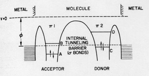
22 SET made from a CdSe nanocrystal The gap is approximately 10-nm wide. There can be several nanocrystals in the gap, but the one that comes closest to the electrodes carries almost all of the current. The heavily doped silicon wafer is used as a gate electrode. The 5.5-nm-diameter nanocrystals are connected to the Au electrodes with 1,6- hexanedithiol, which forms a 1.2-nm-thick barrier. Alivisatos, McEuen et al., Nature 389 (1997) p. 699.
23 Alivisatos, McEuen et al., Nature 389 (1997) p IV characteristics of a CdSe-nanocrystal SET T = 4.2 K

24 Alivisatos, McEuen et al., Nature 389 (1997) p Coulomb diamonds When the conductance is plotted in gray scale as a function of gate voltage and source-drain voltage, there are white diamond shaped regions where the conductance is zero. The plots show how the Coulomb gap varies with gate voltage.
25 Using quantum devices in circuits MOSFETs are only two-state devices (They are either on or off) Quantum devices are multi-state devices. Since they have more functionality than MOSFETs, it is possible that computation could be performed with a smaller number of transistors.
26 Drawbacks and obstacles to nanoelectronic devices In the RTDs the current does not drop to zero in between peaks. The current is very sensitive to the source-drain voltage and the gate voltage. It could be hard to make stable circuits. The devices only show their quantum effects at low temperature because kt must be less than U or ε. The tunneling current is very sensitive to the width of the barrier. The current depends sensitively on the energy levels, which vary substantially with small changes in the size of the potential well.
27 Motivation for using organic devices Every molecule has exactly the same dimensions. Very small devices can be made, so U and ε can be larger than kt at room temperature. Moles of molecules can be made at low cost. Maybe circuits can be made inexpensively using self-assembly techniques.
 electron donor (n-type) In 1974 Aviram and Ratner")
28 Arieh Aviram, Mark Ratner, Chem. Phys. Lett. 29 (1974) p The beginning of molecular electronics Insulating bridge electron acceptor (p-type) electron donor (n-type) In 1974 Aviram and Ratner predicted that molecules with a donor and acceptor would behave like a pn junction.
29 A donor-acceptor junction

30 Forward bias Electrons can easily tunnel Holes can easily tunnel across this barrier. across this barrier. Electrons can tunnel from B to C if there are holes in C. Current flows.

31 Reverse bias Electrons can t tunnel into D. Very little current flows.
32 Goldhaber-Gordon et al. Proc. of IEEE, 85 (1997) p Proposed resonant tunneling in a conjugated molecule A potential problem is that it could be hard to line up energy levels in the source, island and drain since the source and drain have a limited number of energy levels.
33 How can we make these molecular electronic devices?
Single Electron Transistor (SET)
") Single Electron Transistor (SET) SET: e - e - dot A single electron transistor is similar to a normal transistor (below), except 1) the channel is replaced by a small dot. C g 2) the dot is separated from
Single Electron Transistor (SET) SET: e - e - dot A single electron transistor is similar to a normal transistor (below), except 1) the channel is replaced by a small dot. C g 2) the dot is separated from
Single Electron Transistor (SET)
") Single Electron Transistor (SET) e - e - dot C g V g A single electron transistor is similar to a normal transistor (below), except 1) the channel is replaced by a small dot. 2) the dot is separated from
Single Electron Transistor (SET) e - e - dot C g V g A single electron transistor is similar to a normal transistor (below), except 1) the channel is replaced by a small dot. 2) the dot is separated from
ESE370: Circuit-Level Modeling, Design, and Optimization for Digital Systems
 ESE370: Circuit-Level Modeling, Design, and Optimization for Digital Systems Lec 6: September 14, 2015 MOS Model You are Here: Transistor Edition! Previously: simple models (0 and 1 st order) " Comfortable
Molecular Electronics For Fun and Profit(?)
") Molecular Electronics For Fun and Profit(?) Prof. Geoffrey Hutchison Department of Chemistry University of Pittsburgh geoffh@pitt.edu July 22, 2009 http://hutchison.chem.pitt.edu Moore s Law: Transistor
Molecular Electronics For Fun and Profit(?) Prof. Geoffrey Hutchison Department of Chemistry University of Pittsburgh geoffh@pitt.edu July 22, 2009 http://hutchison.chem.pitt.edu Moore s Law: Transistor
Electronic transport in low dimensional systems
 Electronic transport in low dimensional systems For example: 2D system l
! Previously: simple models (0 and 1 st order) " Comfortable with basic functions and circuits. ! This week and next (4 lectures)
 Comfortable with basic functions and circuits. ! This week and next (4 lectures)") ESE370: CircuitLevel Modeling, Design, and Optimization for Digital Systems Lec 6: September 14, 2015 MOS Model You are Here: Transistor Edition! Previously: simple models (0 and 1 st order) " Comfortable
ESE370: CircuitLevel Modeling, Design, and Optimization for Digital Systems Lec 6: September 14, 2015 MOS Model You are Here: Transistor Edition! Previously: simple models (0 and 1 st order) " Comfortable
Lecture 20: Semiconductor Structures Kittel Ch 17, p , extra material in the class notes
 Lecture 20: Semiconductor Structures Kittel Ch 17, p 494-503, 507-511 + extra material in the class notes MOS Structure Layer Structure metal Oxide insulator Semiconductor Semiconductor Large-gap Semiconductor
ESE370: Circuit-Level Modeling, Design, and Optimization for Digital Systems
 ESE370: Circuit-Level Modeling, Design, and Optimization for Digital Systems Lec 6: September 18, 2017 MOS Model You are Here: Transistor Edition! Previously: simple models (0 and 1 st order) " Comfortable
Classification of Solids
 Classification of Solids Classification by conductivity, which is related to the band structure: (Filled bands are shown dark; D(E) = Density of states) Class Electron Density Density of States D(E) Examples
ESE370: Circuit-Level Modeling, Design, and Optimization for Digital Systems. Today MOS MOS. Capacitor. Idea
 ESE370: Circuit-Level Modeling, Design, and Optimization for Digital Systems Day 9: September 26, 2011 MOS Model Today MOS Structure Basic Idea Semiconductor Physics Metals, insulators Silicon lattice
single-electron electron tunneling (SET)
") single-electron electron tunneling (SET) classical dots (SET islands): level spacing is NOT important; only the charging energy (=classical effect, many electrons on the island) quantum dots: : level spacing
single-electron electron tunneling (SET) classical dots (SET islands): level spacing is NOT important; only the charging energy (=classical effect, many electrons on the island) quantum dots: : level spacing
EE130: Integrated Circuit Devices
 EE130: Integrated Circuit Devices (online at http://webcast.berkeley.edu) Instructor: Prof. Tsu-Jae King (tking@eecs.berkeley.edu) TA s: Marie Eyoum (meyoum@eecs.berkeley.edu) Alvaro Padilla (apadilla@eecs.berkeley.edu)
Lectures: Condensed Matter II 1 Electronic Transport in Quantum dots 2 Kondo effect: Intro/theory. 3 Kondo effect in nanostructures
 Lectures: Condensed Matter II 1 Electronic Transport in Quantum dots 2 Kondo effect: Intro/theory. 3 Kondo effect in nanostructures Luis Dias UT/ORNL Lectures: Condensed Matter II 1 Electronic Transport
Semi-Conductors insulators semi-conductors N-type Semi-Conductors P-type Semi-Conductors
 Semi-Conductors In the metal materials considered earlier, the coupling of the atoms together to form the material decouples an electron from each atom setting it free to roam around inside the material.
David J. Starling Penn State Hazleton PHYS 214
 Being virtually killed by a virtual laser in a virtual space is just as effective as the real thing, because you are as dead as you think you are. -Douglas Adams, Mostly Harmless David J. Starling Penn
Chapter 12: Electrical Properties. RA l
 Charge carriers and conduction: Chapter 12: Electrical Properties Charge carriers include all species capable of transporting electrical charge, including electrons, ions, and electron holes. The latter
R. Ludwig and G. Bogdanov RF Circuit Design: Theory and Applications 2 nd edition. Figures for Chapter 6
 R. Ludwig and G. Bogdanov RF Circuit Design: Theory and Applications 2 nd edition Figures for Chapter 6 Free electron Conduction band Hole W g W C Forbidden Band or Bandgap W V Electron energy Hole Valence
There s plenty of room at the bottom! - R.P. Feynman, Nanostructure: a piece of material with at least one dimension less than 100 nm in extent.
 Nanostructures and Nanotechnology There s plenty of room at the bottom! - R.P. Feynman, 1959 Materials behave differently when structured at the nm scale than they do in bulk. Technologies now exist that
UNIVERSITY OF CALIFORNIA College of Engineering Department of Electrical Engineering and Computer Sciences. EECS 130 Professor Ali Javey Fall 2006
 UNIVERSITY OF CALIFORNIA College of Engineering Department of Electrical Engineering and Computer Sciences EECS 130 Professor Ali Javey Fall 2006 Midterm 2 Name: SID: Closed book. Two sheets of notes are
Introduction to Molecular Electronics. Lecture 1: Basic concepts
 Introduction to Molecular Electronics Lecture 1: Basic concepts Conductive organic molecules Plastic can indeed, under certain circumstances, be made to behave very like a metal - a discovery for which
Self-study problems and questions Processing and Device Technology, FFF110/FYSD13
 Self-study problems and questions Processing and Device Technology, FFF110/FYSD13 Version 2016_01 In addition to the problems discussed at the seminars and at the lectures, you can use this set of problems
! Previously: simple models (0 and 1 st order) " Comfortable with basic functions and circuits. ! This week and next (4 lectures)
 Comfortable with basic functions and circuits. ! This week and next (4 lectures)") ESE370: CircuitLevel Modeling, Design, and Optimization for Digital Systems Lec 6: September 18, 2017 MOS Model You are Here: Transistor Edition! Previously: simple models (0 and 1 st order) " Comfortable
ESE370: CircuitLevel Modeling, Design, and Optimization for Digital Systems Lec 6: September 18, 2017 MOS Model You are Here: Transistor Edition! Previously: simple models (0 and 1 st order) " Comfortable
Overview of Nanoelectronic Devices
 Overview of Nanoelectronic Devices DAVID GOLDHABER-GORDON, MICHAEL S. MONTEMERLO, J. CHRISTOPHER LOVE, GREGORY J. OPITECK, AND JAMES C. ELLENBOGEN This paper provides an overview of research developments
CME 300 Properties of Materials. ANSWERS: Homework 9 November 26, As atoms approach each other in the solid state the quantized energy states:
 CME 300 Properties of Materials ANSWERS: Homework 9 November 26, 2011 As atoms approach each other in the solid state the quantized energy states: are split. This splitting is associated with the wave
Quantum Phenomena & Nanotechnology (4B5)
") Quantum Phenomena & Nanotechnology (4B5) The 2-dimensional electron gas (2DEG), Resonant Tunneling diodes, Hot electron transistors Lecture 11 In this lecture, we are going to look at 2-dimensional electron
Quantum Phenomena & Nanotechnology (4B5) The 2-dimensional electron gas (2DEG), Resonant Tunneling diodes, Hot electron transistors Lecture 11 In this lecture, we are going to look at 2-dimensional electron
1 Name: Student number: DEPARTMENT OF PHYSICS AND PHYSICAL OCEANOGRAPHY MEMORIAL UNIVERSITY OF NEWFOUNDLAND. Fall :00-11:00
 1 Name: DEPARTMENT OF PHYSICS AND PHYSICAL OCEANOGRAPHY MEMORIAL UNIVERSITY OF NEWFOUNDLAND Final Exam Physics 3000 December 11, 2012 Fall 2012 9:00-11:00 INSTRUCTIONS: 1. Answer all seven (7) questions.
Current mechanisms Exam January 27, 2012
 Current mechanisms Exam January 27, 2012 There are four mechanisms that typically cause currents to flow: thermionic emission, diffusion, drift, and tunneling. Explain briefly which kind of current mechanisms
LECTURE 23. MOS transistor. 1 We need a smart switch, i.e., an electronically controlled switch. Lecture Digital Circuits, Logic
 LECTURE 23 Lecture 16-20 Digital Circuits, Logic 1 We need a smart switch, i.e., an electronically controlled switch 2 We need a gain element for example, to make comparators. The device of our dreams
Fabrication / Synthesis Techniques
 Quantum Dots Physical properties Fabrication / Synthesis Techniques Applications Handbook of Nanoscience, Engineering, and Technology Ch.13.3 L. Kouwenhoven and C. Marcus, Physics World, June 1998, p.35
Emerging Research Devices: A Study of CNTFET and SET as a replacement for SiMOSFET
 1 Emerging Research Devices: A Study of CNTFET and SET as a replacement for SiMOSFET Mahmoud Lababidi, Krishna Natarajan, Guangyu Sun Abstract Since the development of the Silicon MOSFET, it has been the
MSE 310/ECE 340: Electrical Properties of Materials Fall 2014 Department of Materials Science and Engineering Boise State University
 MSE 310/ECE 340: Electrical Properties of Materials Fall 2014 Department of Materials Science and Engineering Boise State University Practice Final Exam 1 Read the questions carefully Label all figures
Building blocks for nanodevices
 Building blocks for nanodevices Two-dimensional electron gas (2DEG) Quantum wires and quantum point contacts Electron phase coherence Single-Electron tunneling devices - Coulomb blockage Quantum dots (introduction)
Lecture 12: MOS Capacitors, transistors. Context
 Lecture 12: MOS Capacitors, transistors Context In the last lecture, we discussed PN diodes, and the depletion layer into semiconductor surfaces. Small signal models In this lecture, we will apply those
Introduction to semiconductor nanostructures. Peter Kratzer Modern Concepts in Theoretical Physics: Part II Lecture Notes
 Introduction to semiconductor nanostructures Peter Kratzer Modern Concepts in Theoretical Physics: Part II Lecture Notes What is a semiconductor? The Fermi level (chemical potential of the electrons) falls
Chapter 1 Overview of Semiconductor Materials and Physics
 Chapter 1 Overview of Semiconductor Materials and Physics Professor Paul K. Chu Conductivity / Resistivity of Insulators, Semiconductors, and Conductors Semiconductor Elements Period II III IV V VI 2 B
GaN based transistors
 GaN based transistors S FP FP dielectric G SiO 2 Al x Ga 1-x N barrier i-gan Buffer i-sic D Transistors "The Transistor was probably the most important invention of the 20th Century The American Institute
Fig. 8.1 : Schematic for single electron tunneling arrangement. For large system this charge is usually washed out by the thermal noise
 Part 2 : Nanostuctures Lecture 1 : Coulomb blockade and single electron tunneling Module 8 : Coulomb blockade and single electron tunneling Coulomb blockade and single electron tunneling A typical semiconductor
Lecture 20 - Semiconductor Structures
 Lecture 0: Structures Kittel Ch 17, p 494-503, 507-511 + extra material in the class notes MOS Structure metal Layer Structure Physics 460 F 006 Lect 0 1 Outline What is a semiconductor Structure? Created
EN2912C: Future Directions in Computing Lecture 08: Overview of Near-Term Emerging Computing Technologies
 EN2912C: Future Directions in Computing Lecture 08: Overview of Near-Term Emerging Computing Technologies Prof. Sherief Reda Division of Engineering Brown University Fall 2008 1 Near-term emerging computing
Introduction to Semiconductor Physics. Prof.P. Ravindran, Department of Physics, Central University of Tamil Nadu, India
 Introduction to Semiconductor Physics 1 Prof.P. Ravindran, Department of Physics, Central University of Tamil Nadu, India http://folk.uio.no/ravi/cmp2013 Review of Semiconductor Physics Semiconductor fundamentals
From Last Time Important new Quantum Mechanical Concepts. Atoms and Molecules. Today. Symmetry. Simple molecules.
 Today From Last Time Important new Quantum Mechanical Concepts Indistinguishability: Symmetries of the wavefunction: Symmetric and Antisymmetric Pauli exclusion principle: only one fermion per state Spin
Semiconductor Nanowires: Motivation
 Semiconductor Nanowires: Motivation Patterning into sub 50 nm range is difficult with optical lithography. Self-organized growth of nanowires enables 2D confinement of carriers with large splitting of
3/10/2013. Lecture #1. How small is Nano? (A movie) What is Nanotechnology? What is Nanoelectronics? What are Emerging Devices?
 What is Nanotechnology? What is Nanoelectronics? What are Emerging Devices?") EECS 498/598: Nanocircuits and Nanoarchitectures Lecture 1: Introduction to Nanotelectronic Devices (Sept. 5) Lectures 2: ITRS Nanoelectronics Road Map (Sept 7) Lecture 3: Nanodevices; Guest Lecture by
EECS 498/598: Nanocircuits and Nanoarchitectures Lecture 1: Introduction to Nanotelectronic Devices (Sept. 5) Lectures 2: ITRS Nanoelectronics Road Map (Sept 7) Lecture 3: Nanodevices; Guest Lecture by
ITT Technical Institute ET215 Devices I Unit 1
 ITT Technical Institute ET215 Devices I Unit 1 Chapter 1 Chapter 2, Sections 2.1-2.4 Chapter 1 Basic Concepts of Analog Circuits Recall ET115 & ET145 Ohms Law I = V/R If voltage across a resistor increases
Fundamentals of Nanoelectronics: Basic Concepts
 Fundamentals of Nanoelectronics: Basic Concepts Sławomir Prucnal FWIM Page 1 Introduction Outline Electronics in nanoscale Transport Ohms law Optoelectronic properties of semiconductors Optics in nanoscale
CMOS Scaling. Two motivations to scale down. Faster transistors, both digital and analog. To pack more functionality per area. Lower the cost!
 Two motivations to scale down CMOS Scaling Faster transistors, both digital and analog To pack more functionality per area. Lower the cost! (which makes (some) physical sense) Scale all dimensions and
Formation mechanism and Coulomb blockade effect in self-assembled gold quantum dots
 Formation mechanism and Coulomb blockade effect in self-assembled gold quantum dots S. F. Hu a) National Nano Device Laboratories, Hsinchu 300, Taiwan R. L. Yeh and R. S. Liu Department of Chemistry, National
From nanophysics research labs to cell phones. Dr. András Halbritter Department of Physics associate professor
 From nanophysics research labs to cell phones Dr. András Halbritter Department of Physics associate professor Curriculum Vitae Birth: 1976. High-school graduation: 1994. Master degree: 1999. PhD: 2003.
Self-Assembled InAs Quantum Dots
 Self-Assembled InAs Quantum Dots Steve Lyon Department of Electrical Engineering What are semiconductors What are semiconductor quantum dots How do we make (grow) InAs dots What are some of the properties
MOSFET: Introduction
 E&CE 437 Integrated VLSI Systems MOS Transistor 1 of 30 MOSFET: Introduction Metal oxide semiconductor field effect transistor (MOSFET) or MOS is widely used for implementing digital designs Its major
From Last Time. Several important conceptual aspects of quantum mechanics Indistinguishability. Symmetry
 From Last Time Several important conceptual aspects of quantum mechanics Indistinguishability particles are absolutely identical Leads to Pauli exclusion principle (one Fermion / quantum state). Symmetry
Physics and Material Science of Semiconductor Nanostructures
 Physics and Material Science of Semiconductor Nanostructures PHYS 570P Prof. Oana Malis Email: omalis@purdue.edu Course website: http://www.physics.purdue.edu/academic_programs/courses/phys570p/ 1 Introduction
CHAPTER 11 Semiconductor Theory and Devices
 CHAPTER 11 Semiconductor Theory and Devices 11.1 Band Theory of Solids 11.2 Semiconductor Theory 11.3 Semiconductor Devices 11.4 Nanotechnology It is evident that many years of research by a great many
Spintronics. Seminar report SUBMITTED TO: SUBMITTED BY:
 A Seminar report On Spintronics Submitted in partial fulfillment of the requirement for the award of degree of Electronics SUBMITTED TO: SUBMITTED BY: www.studymafia.org www.studymafia.org Preface I have
Semiconductor Theory and Devices
 Semiconductor Theory and Devices Band Theory of Solids Semiconductor Theory Semiconductor Devices Nanotechnology It is evident that many years of research by a great many people, both before and after
MOS Capacitors ECE 2204
 MOS apacitors EE 2204 Some lasses of Field Effect Transistors Metal-Oxide-Semiconductor Field Effect Transistor MOSFET, which will be the type that we will study in this course. Metal-Semiconductor Field
CARLETON UNIVERSITY. FINAL EXAMINATION December 2016
 CARLETON UNIVERSITY FINAL EXAMINATION December 2016 DURATION: 3 HOURS Department Name & Course Number: Electronics 4705 Course Instructor(s): Tom Smy AUTHORIZED MEMORANDA CALCULATOR (Not Programmable)
ELEC 4700 Assignment #2
 ELEC 4700 Assignment #2 Question 1 (Kasop 4.2) Molecular Orbitals and Atomic Orbitals Consider a linear chain of four identical atoms representing a hypothetical molecule. Suppose that each atomic wavefunction
Semiconductor Detectors
 Semiconductor Detectors Summary of Last Lecture Band structure in Solids: Conduction band Conduction band thermal conductivity: E g > 5 ev Valence band Insulator Charge carrier in conductor: e - Charge
Semiconductor Physics fall 2012 problems
 Semiconductor Physics fall 2012 problems 1. An n-type sample of silicon has a uniform density N D = 10 16 atoms cm -3 of arsenic, and a p-type silicon sample has N A = 10 15 atoms cm -3 of boron. For each
Schottky Rectifiers Zheng Yang (ERF 3017,
 ECE442 Power Semiconductor Devices and Integrated Circuits Schottky Rectifiers Zheng Yang (ERF 3017, email: yangzhen@uic.edu) Power Schottky Rectifier Structure 2 Metal-Semiconductor Contact The work function
Spring Semester 2012 Final Exam
 Spring Semester 2012 Final Exam Note: Show your work, underline results, and always show units. Official exam time: 2.0 hours; an extension of at least 1.0 hour will be granted to anyone. Materials parameters
Semiconductor Physics Problems 2015
 Semiconductor Physics Problems 2015 Page and figure numbers refer to Semiconductor Devices Physics and Technology, 3rd edition, by SM Sze and M-K Lee 1. The purest semiconductor crystals it is possible
electronics fundamentals
 electronics fundamentals circuits, devices, and applications THOMAS L. FLOYD DAVID M. BUCHLA Lesson 1: Diodes and Applications Semiconductors Figure 1-1 The Bohr model of an atom showing electrons in orbits
ELECTRONIC DEVICES AND CIRCUITS SUMMARY
 ELECTRONIC DEVICES AND CIRCUITS SUMMARY Classification of Materials: Insulator: An insulator is a material that offers a very low level (or negligible) of conductivity when voltage is applied. Eg: Paper,
EECS130 Integrated Circuit Devices
 EECS130 Integrated Circuit Devices Professor Ali Javey 10/02/2007 MS Junctions, Lecture 2 MOS Cap, Lecture 1 Reading: finish chapter14, start chapter16 Announcements Professor Javey will hold his OH at
EE301 Electronics I , Fall
 EE301 Electronics I 2018-2019, Fall 1. Introduction to Microelectronics (1 Week/3 Hrs.) Introduction, Historical Background, Basic Consepts 2. Rewiev of Semiconductors (1 Week/3 Hrs.) Semiconductor materials
EE 5211 Analog Integrated Circuit Design. Hua Tang Fall 2012
 EE 5211 Analog Integrated Circuit Design Hua Tang Fall 2012 Today s topic: 1. Introduction to Analog IC 2. IC Manufacturing (Chapter 2) Introduction What is Integrated Circuit (IC) vs discrete circuits?
OPTI510R: Photonics. Khanh Kieu College of Optical Sciences, University of Arizona Meinel building R.626
 OPTI510R: Photonics Khanh Kieu College of Optical Sciences, University of Arizona kkieu@optics.arizona.edu Meinel building R.626 Announcements HW#3 is assigned due Feb. 20 st Mid-term exam Feb 27, 2PM
Midterm I - Solutions
 UNIVERSITY OF CALIFORNIA College of Engineering Department of Electrical Engineering and Computer Sciences EECS 130 Spring 2008 Professor Chenming Hu Midterm I - Solutions Name: SID: Grad/Undergrad: Closed
KATIHAL FİZİĞİ MNT-510
 KATIHAL FİZİĞİ MNT-510 YARIİLETKENLER Kaynaklar: Katıhal Fiziği, Prof. Dr. Mustafa Dikici, Seçkin Yayıncılık Katıhal Fiziği, Şakir Aydoğan, Nobel Yayıncılık, Physics for Computer Science Students: With
Tunneling transport. Courtesy Prof. S. Sawyer, RPI Also Davies Ch. 5
 unneling transport Courtesy Prof. S. Sawyer, RPI Also Davies Ch. 5 Electron transport properties l e : electronic mean free path l φ : phase coherence length λ F : Fermi wavelength ecture Outline Important
News from NBIA. Condensed Matter Physics: from new materials to quantum technology. time. Mark Rudner
 News from NBIA Condensed Matter Physics: from new materials to quantum technology Mark Rudner time ~100 years after Bohr, the basic laws and players are established 1913 2013 Image from www.periodni.com
Lecture 0: Introduction
 Lecture 0: Introduction Introduction q Integrated circuits: many transistors on one chip q Very Large Scale Integration (VLSI): bucketloads! q Complementary Metal Oxide Semiconductor Fast, cheap, low power
ESE 570: Digital Integrated Circuits and VLSI Fundamentals
 ESE 570: Digital Integrated Circuits and VLSI Fundamentals Lec 4: January 23, 2018 MOS Transistor Theory, MOS Model Penn ESE 570 Spring 2018 Khanna Lecture Outline! CMOS Process Enhancements! Semiconductor
Solid State Device Fundamentals
 Solid State Device Fundamentals ENS 345 Lecture Course by Alexander M. Zaitsev alexander.zaitsev@csi.cuny.edu Tel: 718 982 2812 Office 4N101b 1 Outline - Goals of the course. What is electronic device?
ECE 340 Lecture 39 : MOS Capacitor II
 ECE 340 Lecture 39 : MOS Capacitor II Class Outline: Effects of Real Surfaces Threshold Voltage MOS Capacitance-Voltage Analysis Things you should know when you leave Key Questions What are the effects
Stretching the Barriers An analysis of MOSFET Scaling. Presenters (in order) Zeinab Mousavi Stephanie Teich-McGoldrick Aseem Jain Jaspreet Wadhwa
 Zeinab Mousavi Stephanie Teich-McGoldrick Aseem Jain Jaspreet Wadhwa") Stretching the Barriers An analysis of MOSFET Scaling Presenters (in order) Zeinab Mousavi Stephanie Teich-McGoldrick Aseem Jain Jaspreet Wadhwa Why Small? Higher Current Lower Gate Capacitance Higher
Stretching the Barriers An analysis of MOSFET Scaling Presenters (in order) Zeinab Mousavi Stephanie Teich-McGoldrick Aseem Jain Jaspreet Wadhwa Why Small? Higher Current Lower Gate Capacitance Higher
Introduction to Nanotechnology Chapter 5 Carbon Nanostructures Lecture 1
 Introduction to Nanotechnology Chapter 5 Carbon Nanostructures Lecture 1 ChiiDong Chen Institute of Physics, Academia Sinica chiidong@phys.sinica.edu.tw 02 27896766 Carbon contains 6 electrons: (1s) 2,
Nanoscience and Molecular Engineering (ChemE 498A) Semiconductor Nano Devices
 Semiconductor Nano Devices") Reading: The first two readings cover the questions to bands and quasi-electrons/holes. See also problem 4. General Questions: 1. What is the main difference between a metal and a semiconductor or insulator,
Reading: The first two readings cover the questions to bands and quasi-electrons/holes. See also problem 4. General Questions: 1. What is the main difference between a metal and a semiconductor or insulator,
ρ ρ LED access resistances d A W d s n s p p p W the output window size p-layer d p series access resistance d n n-layer series access resistance
 LED access resistances W the output window size p-layer series access resistance d p n-layer series access resistance d n The n-layer series access resistance R = ρ s n where the resistivity of the n-layer
Section 12: Intro to Devices
 Section 12: Intro to Devices Extensive reading materials on reserve, including Robert F. Pierret, Semiconductor Device Fundamentals EE143 Ali Javey Bond Model of Electrons and Holes Si Si Si Si Si Si Si
are microscopically large but macroscopically small contacts which may be connected to a battery to provide the bias voltage across the junction.
 At present, we observe a long-lasting process of miniaturization of electronic devices. The ultimate limit for the miniaturization of electronic components is set by the atomic scale. However, in the case
Measuring charge transport through molecules
 Measuring charge transport through molecules utline Indirect methods 1. ptical techniques 2. Electrochemical techniques Direct methods 1. Scanning probe techniques 2. In-plane electrodes 3. Break junctions
A SEMICONDUCTOR DIODE. P-N Junction
 A SEMICONDUCTOR DIODE P-N Junction Analog Electronics Pujianto Department of Physics Edu. State University of Yogyakarta A Semiconductor Devices A Semiconductor devices can be defined as a unit which consists,
Demonstration of a functional quantum-dot cellular automata cell
 Demonstration of a functional quantum-dot cellular automata cell Islamshah Amlani, a) Alexei O. Orlov, Gregory L. Snider, Craig S. Lent, and Gary H. Bernstein Department of Electrical Engineering, University
Section 12: Intro to Devices
 Section 12: Intro to Devices Extensive reading materials on reserve, including Robert F. Pierret, Semiconductor Device Fundamentals Bond Model of Electrons and Holes Si Si Si Si Si Si Si Si Si Silicon
A final review session will be offered on Thursday, May 10 from 10AM to 12noon in 521 Cory (the Hogan Room).
.") A final review session will be offered on Thursday, May 10 from 10AM to 12noon in 521 Cory (the Hogan Room). The Final Exam will take place from 12:30PM to 3:30PM on Saturday May 12 in 60 Evans.» All of
A final review session will be offered on Thursday, May 10 from 10AM to 12noon in 521 Cory (the Hogan Room). The Final Exam will take place from 12:30PM to 3:30PM on Saturday May 12 in 60 Evans.» All of
Electronic Circuits 1. Transistor Devices. Contents BJT and FET Characteristics Operations. Prof. C.K. Tse: Transistor devices
 Electronic Circuits 1 Transistor Devices Contents BJT and FET Characteristics Operations 1 What is a transistor? Three-terminal device whose voltage-current relationship is controlled by a third voltage
CLASS 12th. Semiconductors
 CLASS 12th Semiconductors 01. Distinction Between Metals, Insulators and Semi-Conductors Metals are good conductors of electricity, insulators do not conduct electricity, while the semiconductors have
Electrical and Optical Properties. H.Hofmann
 Introduction to Nanomaterials Electrical and Optical Properties H.Hofmann Electrical Properties Ohm: G= σw/l where is the length of the conductor, measured in meters [m], A is the cross-section area of
Solid State Device Fundamentals
 Solid State Device Fundamentals ENS 345 Lecture Course by Alexander M. Zaitsev alexander.zaitsev@csi.cuny.edu Tel: 718 982 2812 Office 4N101b 1 Outline - Goals of the course. What is electronic device?
Chapter 3 Basics Semiconductor Devices and Processing
 Chapter 3 Basics Semiconductor Devices and Processing Hong Xiao, Ph. D. www2.austin.cc.tx.us/hongxiao/book.htm Hong Xiao, Ph. D. www2.austin.cc.tx.us/hongxiao/book.htm 1 Objectives Identify at least two
Surfaces, Interfaces, and Layered Devices
 Surfaces, Interfaces, and Layered Devices Building blocks for nanodevices! W. Pauli: God made solids, but surfaces were the work of Devil. Surfaces and Interfaces 1 Interface between a crystal and vacuum
Digital Electronics Part II - Circuits
 Digital Electronics Part - Circuits Dr.. J. Wassell Gates from Transistors ntroduction Logic circuits are non-linear, consequently we will introduce a graphical technique for analysing such circuits The
ESE 570: Digital Integrated Circuits and VLSI Fundamentals
 ESE 570: Digital Integrated Circuits and VLSI Fundamentals Lec 4: January 24, 2017 MOS Transistor Theory, MOS Model Penn ESE 570 Spring 2017 Khanna Lecture Outline! Semiconductor Physics " Band gaps "
8. Schottky contacts / JFETs
 Technische Universität Graz Institute of Solid State Physics 8. Schottky contacts / JFETs Nov. 21, 2018 Technische Universität Graz Institute of Solid State Physics metal - semiconductor contacts Photoelectric
Lecture 3: Heterostructures, Quasielectric Fields, and Quantum Structures
 Lecture 3: Heterostructures, Quasielectric Fields, and Quantum Structures MSE 6001, Semiconductor Materials Lectures Fall 2006 3 Semiconductor Heterostructures A semiconductor crystal made out of more
2) Atom manipulation. Xe / Ni(110) Model: Experiment:
 Atom manipulation. Xe / Ni(110) Model: Experiment:") 2) Atom manipulation D. Eigler & E. Schweizer, Nature 344, 524 (1990) Xe / Ni(110) Model: Experiment: G.Meyer, et al. Applied Physics A 68, 125 (1999) First the tip is approached close to the adsorbate
2) Atom manipulation D. Eigler & E. Schweizer, Nature 344, 524 (1990) Xe / Ni(110) Model: Experiment: G.Meyer, et al. Applied Physics A 68, 125 (1999) First the tip is approached close to the adsorbate
EECS143 Microfabrication Technology
 EECS143 Microfabrication Technology Professor Ali Javey Introduction to Materials Lecture 1 Evolution of Devices Yesterday s Transistor (1947) Today s Transistor (2006) Why Semiconductors? Conductors e.g