Graphene The Search For Two Dimensions. Christopher Scott Friedline Arizona State University
|
|
|
- Julius Thornton
- 5 years ago
- Views:
Transcription

1 Graphene The Search For Two Dimensions Christopher Scott Friedline Arizona State University

2 What Is Graphene? Single atomic layer of graphite arranged in a honeycomb crystal lattice Consists of sp 2 -bonded carbon atoms with bond length approximately 1.42 angstroms Basic structural element for all other graphitic materials


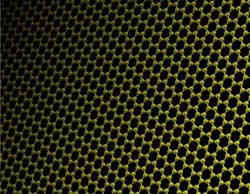
3 Graphitic Materials 0-D Fullerenes (Buckyballs) 1-D Carbon Nanotubes 2-D Graphene 3-D Graphite
4 Why Study Graphene? Graphene has many new and unusual properties that lead to the current excitement of its study. Linear Dispersion Relation Massless Electrons Electron Mobility & Minimum Conductivity Quantum Hall Effect Possibilities For New & Old Physics


5 Linear Dispersion Relation Most condensed matter electron transport is described by the Schrodinger Equation. This is not the case for Graphene. The energy-momentum relation is linear near the six corners in graphene s Brillouin zone. In this region, electrons behave like relativistic particles having zero effective mass and behave according to Dirac s Equation for spin ½ particles. The Fermi velocity (v f ) is 10 6 m/s. E r = hvf k
6 Electron Mobility & Minimum Conductivity Electron mobility in graphene is remarkably high at room temperature ( Ω m) vs 10 ( Ω m) The resistivity of graphene is less than silver, the lowest substance known at room temperature ( Ω m) Should be zero carrier density at Dirac points yet there exists a minimum conductivity. 4e 2 4e 2? h πh The origin of minimum conductivity is still unclear.

7 Quantum Hall Effect Potential difference on the opposite sides of an electrical conductor through which an electric current is flowing, created by a magnetic field applied perpendicular to the current. Quantum hall effect is seen in 2-D objects with quantized values of conductivity. Bi-layer agrees with standard effect while mono-layer has a shift of ½. Graphene is the only known material that sees this effect at room temperature. σ xy σ xy e 2 =±4 h N e =± h 2 ( N )

8 Possibilities For New & Old Physics Relativistic quantum mechanics 2-D Dirac equations Klein Paradox Veselago Lens Table Top Relativity


9 Future Applications Graphenium microprocessors order of magnitude better than Si Graphene transistors more effective the smaller they get Graphene powder in batteries to replace carbon nanofibers Optical properties allow to be used to improve plasma displays, LCDs and touch screens Single molecule gas detection

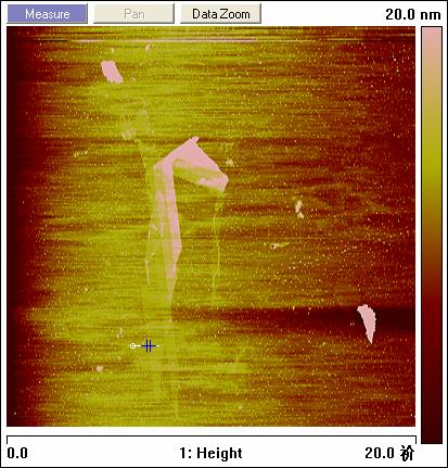
10 Looking For 2-Dimensions In a 3-D Universe Currently, graphene is the most expensive materials on earth. As of April, 2008 a piece of graphene the size of the cross section of a human hair cost $1,000. Producing graphene is easy, finding it is the real challenge. Visual and Atomic Force Microscopy
11 How is Graphene Made and Found in the Lab One of the hardest aspects of working with graphene is being able to create and find it successfully and consistently. Preparing SiO 2 wafer Rubbing techniques Scotch tape method Optical microscopy AFM


12 Preparing SiO 2 Wafer Diamond Pen Acetone Sonication IPA Rinse Compressed Air BOE Etching Piranha Etching 280 vs. 300 nm Oxide
13 Rubbing Techniques The first real challenge of depositing graphene flakes onto SiO 2 is to find a reliable technique that works consistently. Gentle to forceful rubbing with tweezers Graphite sandwich Liquid deposition water, acetone, IPA Heated wafer Cleaving


14 Scotch Tape Method Developed by researchers at Manchester University Single piece of graphite cleaved multiple times quickly Fresh atomic layers at each graphite site Ability to create multiple samples with less time and material


15 Scotch Tape Method
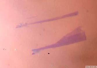
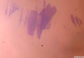
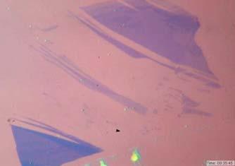
16 Optical Microscopy Graphene can be viewed optically with minimal magnification Approximate thickness is determined by color (black, white, blue, purple, pink) Slow process of scanning, pictures and documenting 4x, 10x, 20x, 40x, 100x magnification 5um


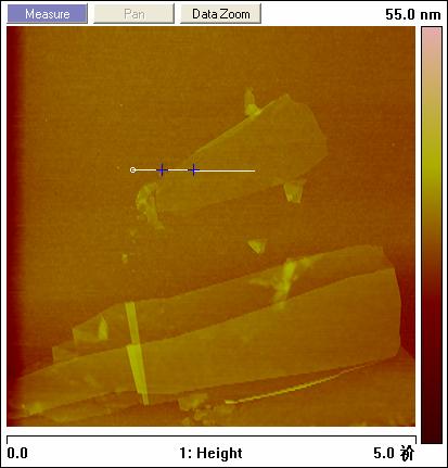
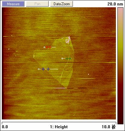
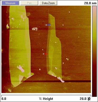
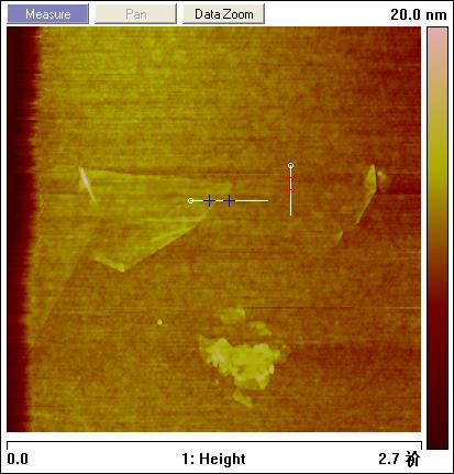
17 Atomic Force Microscopy Measures height to give a topological picture Derivative gives a 3-D picture of surface Cantilever oscillates at or near resonant frequency Repelled by van der Waals force Reflected laser off back of cantilever records data

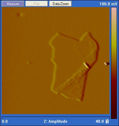
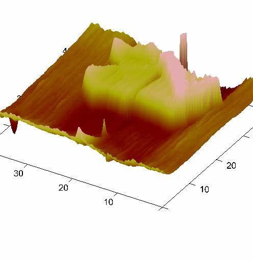
18 Atomic Force Microscopy
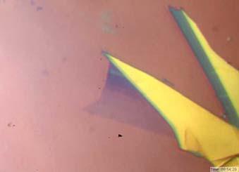
19 Sample (1)csf Multiple POI s Varied thickness Possible single layer


20 Colloidal Gold and Fluorescence Microscopy Sample illuminated with specific wavelength of light Light is absorbed by gold and emits a longer wavelength Colloidal gold is sensitive to dielectric materials Should be a large difference in wavelength between single and bi-layer graphene


21 Experimenting With Gold Spun onto substrate Viewed with AFM Goal: Deposit gold on or around graphene


22 Setback Discovery Spinning gold colloid affects thinner pieces of graphene causing it to fold and lose its integrity. What if gold is spun first and then graphene is deposited?


23 Single Layer Graphene Initial results showed multiple POI s with confirmed single layer graphene. Gold colloid was on and around all POI s. What caused this?


24 Friction & Anchors Gold on the substrate could act as a source of friction Graphite moves gold around causes them to clump Large enough pieces finally grab onto the substrate and anchor down large layers of graphite
25 Repeatable 0.789nm 0.734nm 0.874nm 0.821nm 0.054nm 0.792nm 1.189nm 1.201nm 0.748nm

26 Improvement On Original Technique Gold Original Technique 5 Pieces of Graphene 1 Possible Piece of Graphene


27 Continued production of graphene Fluorescence microscopy Devices Growing VO 2 on graphene Using gold colloid as VO 2 seeds Future Research


28 Special Thanks David Cobden Advisor Jiang Wei Zenghui Wang Jae Hyung Park (Not Pictured) Jacob Beedle Peter Morse Geeta Yadav (Not Pictured)
29 Questions?
Quantum Electrodynamics in Graphene
 Quantum Electrodynamics in Graphene Judy G. Cherian Kutztown University of PA Physics REU 2006 Univ. Of Washington Advisor- Dr. David Cobden Dr. Sam Fain Andrew Jones Graphene, a single layer of graphite,
Overview. Carbon in all its forms. Background & Discovery Fabrication. Important properties. Summary & References. Overview of current research
 Graphene Prepared for Solid State Physics II Pr Dagotto Spring 2009 Laurene Tetard 03/23/09 Overview Carbon in all its forms Background & Discovery Fabrication Important properties Overview of current
GRAPHENE the first 2D crystal lattice
 GRAPHENE the first 2D crystal lattice dimensionality of carbon diamond, graphite GRAPHENE realized in 2004 (Novoselov, Science 306, 2004) carbon nanotubes fullerenes, buckyballs what s so special about
Carbon based Nanoscale Electronics
 Carbon based Nanoscale Electronics 09 02 200802 2008 ME class Outline driving force for the carbon nanomaterial electronic properties of fullerene exploration of electronic carbon nanotube gold rush of
Graphene. Tianyu Ye November 30th, 2011
 Graphene Tianyu Ye November 30th, 2011 Outline What is graphene? How to make graphene? (Exfoliation, Epitaxial, CVD) Is it graphene? (Identification methods) Transport properties; Other properties; Applications;
Seminars in Nanosystems - I
 Seminars in Nanosystems - I Winter Semester 2011/2012 Dr. Emanuela Margapoti Emanuela.Margapoti@wsi.tum.de Dr. Gregor Koblmüller Gregor.Koblmueller@wsi.tum.de Seminar Room at ZNN 1 floor Topics of the
Graphene - most two-dimensional system imaginable
 Graphene - most two-dimensional system imaginable A suspended sheet of pure graphene a plane layer of C atoms bonded together in a honeycomb lattice is the most two-dimensional system imaginable. A.J.
Initial Stages of Growth of Organic Semiconductors on Graphene
 Initial Stages of Growth of Organic Semiconductors on Graphene Presented by: Manisha Chhikara Supervisor: Prof. Dr. Gvido Bratina University of Nova Gorica Outline Introduction to Graphene Fabrication
The many forms of carbon
 The many forms of carbon Carbon is not only the basis of life, it also provides an enormous variety of structures for nanotechnology. This versatility is connected to the ability of carbon to form two
Nanostructures. Lecture 13 OUTLINE
 Nanostructures MTX9100 Nanomaterials Lecture 13 OUTLINE -What is quantum confinement? - How can zero-dimensional materials be used? -What are one dimensional structures? -Why does graphene attract so much
Scripts for High School Visits to the Herman Group at Columbia University
 Scripts for High School Visits to the Herman Group at Columbia University Evan Spotte-Smith, Jiayang Hu, and Irving P. Herman April, 2017; updated June, 2017 These presentations were developed for visits
Graphite, graphene and relativistic electrons
 Graphite, graphene and relativistic electrons Introduction Physics of E. graphene Y. Andrei Experiments Rutgers University Transport electric field effect Quantum Hall Effect chiral fermions STM Dirac
Monolayer Semiconductors
 Monolayer Semiconductors Gilbert Arias California State University San Bernardino University of Washington INT REU, 2013 Advisor: Xiaodong Xu (Dated: August 24, 2013) Abstract Silicon may be unable to
Supporting Information Available:
 Supporting Information Available: Photoresponsive and Gas Sensing Field-Effect Transistors based on Multilayer WS 2 Nanoflakes Nengjie Huo 1, Shengxue Yang 1, Zhongming Wei 2, Shu-Shen Li 1, Jian-Bai Xia
Imaging Carbon materials with correlative Raman-SEM microscopy. Introduction. Raman, SEM and FIB within one chamber. Diamond.
 Imaging Carbon materials with correlative Raman-SEM microscopy Application Example Carbon materials are widely used in many industries for their exceptional properties. Electric conductance, light weight,
The Low Temperature Physics of Thin Films Superconducting Tin and Monolayer Graphene
 The Low Temperature Physics of Thin Films Superconducting Tin and Monolayer Graphene Abstract: The aim of this project was to investigate how the electrical resistance of a conductor changes if it is deposited
GRAPHENE ON THE Si-FACE OF SILICON CARBIDE USER MANUAL
 GRAPHENE ON THE Si-FACE OF SILICON CARBIDE USER MANUAL 1. INTRODUCTION Silicon Carbide (SiC) is a wide band gap semiconductor that exists in different polytypes. The substrate used for the fabrication
SUPPLEMENTARY INFORMATION
 SUPPLEMENTARY INFORMATION Facile Synthesis of High Quality Graphene Nanoribbons Liying Jiao, Xinran Wang, Georgi Diankov, Hailiang Wang & Hongjie Dai* Supplementary Information 1. Photograph of graphene
Supplementary Figure 1: Micromechanical cleavage of graphene on oxygen plasma treated Si/SiO2. Supplementary Figure 2: Comparison of hbn yield.
 1 2 3 4 Supplementary Figure 1: Micromechanical cleavage of graphene on oxygen plasma treated Si/SiO 2. Optical microscopy images of three examples of large single layer graphene flakes cleaved on a single
Kavli Workshop for Journalists. June 13th, CNF Cleanroom Activities
 Kavli Workshop for Journalists June 13th, 2007 CNF Cleanroom Activities Seeing nm-sized Objects with an SEM Lab experience: Scanning Electron Microscopy Equipment: Zeiss Supra 55VP Scanning electron microscopes
A BIT OF MATERIALS SCIENCE THEN PHYSICS
 GRAPHENE AND OTHER D ATOMIC CRYSTALS Andre Geim with many thanks to K. Novoselov, S. Morozov, D. Jiang, F. Schedin, I. Grigorieva, J. Meyer, M. Katsnelson A BIT OF MATERIALS SCIENCE THEN PHYSICS CARBON
Graphene FETs EE439 FINAL PROJECT. Yiwen Meng Su Ai
 Graphene FETs EE439 FINAL PROJECT Yiwen Meng Su Ai Introduction What is Graphene? An atomic-scale honeycomb lattice made of carbon atoms Before 2004, Hypothetical Carbon Structure Until 2004, physicists
SOLID STATE PHYSICS. Second Edition. John Wiley & Sons. J. R. Hook H. E. Hall. Department of Physics, University of Manchester
 SOLID STATE PHYSICS Second Edition J. R. Hook H. E. Hall Department of Physics, University of Manchester John Wiley & Sons CHICHESTER NEW YORK BRISBANE TORONTO SINGAPORE Contents Flow diagram Inside front
Imaging Methods: Scanning Force Microscopy (SFM / AFM)
") Imaging Methods: Scanning Force Microscopy (SFM / AFM) The atomic force microscope (AFM) probes the surface of a sample with a sharp tip, a couple of microns long and often less than 100 Å in diameter.
Imaging Methods: Scanning Force Microscopy (SFM / AFM) The atomic force microscope (AFM) probes the surface of a sample with a sharp tip, a couple of microns long and often less than 100 Å in diameter.
SiC Graphene Suitable For Quantum Hall Resistance Metrology.
 SiC Graphene Suitable For Quantum Hall Resistance Metrology. Samuel Lara-Avila 1, Alexei Kalaboukhov 1, Sara Paolillo, Mikael Syväjärvi 3, Rositza Yakimova 3, Vladimir Fal'ko 4, Alexander Tzalenchuk 5,
Transient Photocurrent Measurements of Graphene Related Materials
 Transient Photocurrent Measurements of Graphene Related Materials P. Srinivasa Rao Mentor: Prof. dr. Gvido Bratina Laboratory of Organic Matter Physics University of Nova Gorica 1 Contents: 1. Electrical
In today s lecture, we will cover:
 In today s lecture, we will cover: Metal and Metal oxide Nanoparticles Semiconductor Nanocrystals Carbon Nanotubes 1 Week 2: Nanoparticles Goals for this section Develop an understanding of the physical
Nanosphere Lithography
 Nanosphere Lithography Derec Ciafre 1, Lingyun Miao 2, and Keita Oka 1 1 Institute of Optics / 2 ECE Dept. University of Rochester Abstract Nanosphere Lithography is quickly emerging as an efficient, low
The Solid State. Phase diagrams Crystals and symmetry Unit cells and packing Types of solid
 The Solid State Phase diagrams Crystals and symmetry Unit cells and packing Types of solid Learning objectives Apply phase diagrams to prediction of phase behaviour Describe distinguishing features of
SUPPLEMENTARY INFORMATION
 Direct Visualization of Large-Area Graphene Domains and Boundaries by Optical Birefringency Dae Woo Kim 1,*, Yun Ho Kim 1,2,*, Hyeon Su Jeong 1, Hee-Tae Jung 1 * These authors contributed equally to this
Supporting Information. by Hexagonal Boron Nitride
 Supporting Information High Velocity Saturation in Graphene Encapsulated by Hexagonal Boron Nitride Megan A. Yamoah 1,2,, Wenmin Yang 1,3, Eric Pop 4,5,6, David Goldhaber-Gordon 1 * 1 Department of Physics,
Session V: Graphene. Matteo Bruna CAMBRIDGE UNIVERSITY DEPARTMENT OF ENGINEERING
 Session V: Graphene Matteo Bruna Graphene: Material in the Flatland Graphite Graphene Properties: Thinnest imaginable material Good(and tunable) electrical conductor Strongest ever measured Stiffest known
Supplementary Figure S1. AFM images of GraNRs grown with standard growth process. Each of these pictures show GraNRs prepared independently,
 Supplementary Figure S1. AFM images of GraNRs grown with standard growth process. Each of these pictures show GraNRs prepared independently, suggesting that the results is reproducible. Supplementary Figure
Supplementary Figure 1 Dark-field optical images of as prepared PMMA-assisted transferred CVD graphene films on silicon substrates (a) and the one
 and the one") Supplementary Figure 1 Dark-field optical images of as prepared PMMA-assisted transferred CVD graphene films on silicon substrates (a) and the one after PBASE monolayer growth (b). 1 Supplementary Figure
Supplementary Figure 1 Dark-field optical images of as prepared PMMA-assisted transferred CVD graphene films on silicon substrates (a) and the one after PBASE monolayer growth (b). 1 Supplementary Figure
From nanophysics research labs to cell phones. Dr. András Halbritter Department of Physics associate professor
 From nanophysics research labs to cell phones Dr. András Halbritter Department of Physics associate professor Curriculum Vitae Birth: 1976. High-school graduation: 1994. Master degree: 1999. PhD: 2003.
TRANSVERSE SPIN TRANSPORT IN GRAPHENE
 International Journal of Modern Physics B Vol. 23, Nos. 12 & 13 (2009) 2641 2646 World Scientific Publishing Company TRANSVERSE SPIN TRANSPORT IN GRAPHENE TARIQ M. G. MOHIUDDIN, A. A. ZHUKOV, D. C. ELIAS,
Graphene FETs with Combined Structure and Transparent Top
 Available online at www.sciencedirect.com Physics Procedia 32 (2012 ) 869 874 18th International Vacuum Congress (IVC-18) Graphene FETs with Combined Structure and Transparent Top Yuanlin Yuan a, Zhen
So why is sodium a metal? Tungsten Half-filled 5d band & half-filled 6s band. Insulators. Interaction of metals with light?
 Bonding in Solids: Metals, Insulators, & CHEM 107 T. Hughbanks Delocalized bonding in Solids Think of a pure solid as a single, very large molecule. Use our bonding pictures to try to understand properties.
Carbon nanomaterials. Gavin Lawes Wayne State University.
 Carbon nanomaterials Gavin Lawes Wayne State University glawes@wayne.edu Outline 1. Carbon structures 2. Carbon nanostructures 3. Potential applications for Carbon nanostructures Periodic table from bpc.edu
A. Optimizing the growth conditions of large-scale graphene films
 1 A. Optimizing the growth conditions of large-scale graphene films Figure S1. Optical microscope images of graphene films transferred on 300 nm SiO 2 /Si substrates. a, Images of the graphene films grown
Ferromagnetism and Anomalous Hall Effect in Graphene
 Ferromagnetism and Anomalous Hall Effect in Graphene Jing Shi Department of Physics & Astronomy, University of California, Riverside Graphene/YIG Introduction Outline Proximity induced ferromagnetism Quantized
Physical Properties of Mono-layer of
 Chapter 3 Physical Properties of Mono-layer of Silicene The fascinating physical properties[ 6] associated with graphene have motivated many researchers to search for new graphene-like two-dimensional
Lecture 20: Semiconductor Structures Kittel Ch 17, p , extra material in the class notes
 Lecture 20: Semiconductor Structures Kittel Ch 17, p 494-503, 507-511 + extra material in the class notes MOS Structure Layer Structure metal Oxide insulator Semiconductor Semiconductor Large-gap Semiconductor
The Raman Spectroscopy of Graphene and the Determination of Layer Thickness
 Application Note: 52252 The Raman Spectroscopy of Graphene and the Determination of Layer Thickness Mark Wall, Ph.D., Thermo Fisher Scientific, Madison, WI, USA Key Words DXR Raman Microscope 2D Band D
Graphene electronics
 Graphene electronics Alberto Morpurgo Main collaborators J. Oostinga, H. Heersche, P. Jarillo Herrero, S. Russo, M. Craciun, L. Vandersypen, S. Tarucha, R. Danneau, P. Hakkonen A simple tight-binding H
3-month progress Report
 3-month progress Report Graphene Devices and Circuits Supervisor Dr. P.A Childs Table of Content Abstract... 1 1. Introduction... 1 1.1 Graphene gold rush... 1 1.2 Properties of graphene... 3 1.3 Semiconductor
Supplementary Figure 1. Magneto-transport characteristics of topological semimetal Cd 3 As 2 microribbon. (a) Measured resistance (R) as a function
 Measured resistance (R) as a function") Supplementary Figure 1. Magneto-transport characteristics of topological semimetal Cd 3 As 2 microribbon. (a) Measured resistance (R) as a function of temperature (T) at zero magnetic field. (b) Magnetoresistance
Supplementary Figure 1. Magneto-transport characteristics of topological semimetal Cd 3 As 2 microribbon. (a) Measured resistance (R) as a function of temperature (T) at zero magnetic field. (b) Magnetoresistance
Semiconductors and Optoelectronics. Today Semiconductors Acoustics. Tomorrow Come to CH325 Exercises Tours
 Semiconductors and Optoelectronics Advanced Physics Lab, PHYS 3600 Don Heiman, Northeastern University, 2017 Today Semiconductors Acoustics Tomorrow Come to CH325 Exercises Tours Semiconductors and Optoelectronics
Graphene: Plane and Simple Electrical Metrology?
 Graphene: Plane and Simple Electrical Metrology? R. E. Elmquist, F. L. Hernandez-Marquez, M. Real, T. Shen, D. B. Newell, C. J. Jacob, and G. R. Jones, Jr. National Institute of Standards and Technology,
SUPPLEMENTARY INFORMATION
 DOI: 1.138/NMAT3449 Topological crystalline insulator states in Pb 1 x Sn x Se Content S1 Crystal growth, structural and chemical characterization. S2 Angle-resolved photoemission measurements at various
Modern Physics for Scientists and Engineers International Edition, 4th Edition
 Modern Physics for Scientists and Engineers International Edition, 4th Edition http://optics.hanyang.ac.kr/~shsong 1. THE BIRTH OF MODERN PHYSICS 2. SPECIAL THEORY OF RELATIVITY 3. THE EXPERIMENTAL BASIS
Transport through Andreev Bound States in a Superconductor-Quantum Dot-Graphene System
 Transport through Andreev Bound States in a Superconductor-Quantum Dot-Graphene System Nadya Mason Travis Dirk, Yung-Fu Chen, Cesar Chialvo Taylor Hughes, Siddhartha Lal, Bruno Uchoa Paul Goldbart University
Spin Injection into a Graphene Thin Film at Room Temperature
 Spin Injection into a Graphene Thin Film at Room Temperature Megumi Ohishi, Masashi Shiraishi*, Ryo Nouchi, Takayuki Nozaki, Teruya Shinjo, and Yoshishige Suzuki Graduate School of Engineering Science,
Confocal Microscopy Imaging of Single Emitter Fluorescence and Hanbury Brown and Twiss Photon Antibunching Setup
 1 Confocal Microscopy Imaging of Single Emitter Fluorescence and Hanbury Brown and Twiss Photon Antibunching Setup Abstract Jacob Begis The purpose of this lab was to prove that a source of light can be
TOPOLOGICAL BANDS IN GRAPHENE SUPERLATTICES
 TOPOLOGICAL BANDS IN GRAPHENE SUPERLATTICES 1) Berry curvature in superlattice bands 2) Energy scales for Moire superlattices 3) Spin-Hall effect in graphene Leonid Levitov (MIT) @ ISSP U Tokyo MIT Manchester
Graphene. L. Tetard 1,2. (Dated: April 7, 2009) 1 Oak Ridge National Laboratory, Oak Ridge, TN USA
 1 Oak Ridge National Laboratory, Oak Ridge, TN USA") Graphene L. Tetard 1,2 1 Oak Ridge National Laboratory, Oak Ridge, TN 37831-6123 USA 2 Department of Physics, University of Tennessee, Knoxville, TN 37996, USA (Dated: April 7, 2009) 1 Diamond, graphite,
Graphene L. Tetard 1,2 1 Oak Ridge National Laboratory, Oak Ridge, TN 37831-6123 USA 2 Department of Physics, University of Tennessee, Knoxville, TN 37996, USA (Dated: April 7, 2009) 1 Diamond, graphite,
Supplementary Materials for
 advances.sciencemag.org/cgi/content/full/4/9/eaat8355/dc1 Supplementary Materials for Electronic structures and unusually robust bandgap in an ultrahigh-mobility layered oxide semiconductor, Bi 2 O 2 Se
Supporting Information
 Supporting Information Real-Time Monitoring of Insulin Using a Graphene Field-Effect Transistor Aptameric Nanosensor Zhuang Hao, a,b Yibo Zhu, a Xuejun Wang, a Pavana G. Rotti, c,d Christopher DiMarco,
Electronic properties of graphene. Jean-Noël Fuchs Laboratoire de Physique des Solides Université Paris-Sud (Orsay)
") Electronic properties of graphene Jean-Noël Fuchs Laboratoire de Physique des Solides Université Paris-Sud (Orsay) Cargèse, September 2012 3 one-hour lectures in 2 x 1,5h on electronic properties of graphene
Electronic properties of graphene Jean-Noël Fuchs Laboratoire de Physique des Solides Université Paris-Sud (Orsay) Cargèse, September 2012 3 one-hour lectures in 2 x 1,5h on electronic properties of graphene
Classification of Solids
 Classification of Solids Classification by conductivity, which is related to the band structure: (Filled bands are shown dark; D(E) = Density of states) Class Electron Density Density of States D(E) Examples
Chapter 37 Early Quantum Theory and Models of the Atom. Copyright 2009 Pearson Education, Inc.
 Chapter 37 Early Quantum Theory and Models of the Atom Planck s Quantum Hypothesis; Blackbody Radiation Photon Theory of Light and the Photoelectric Effect Energy, Mass, and Momentum of a Photon Compton
Lecture 20 - Semiconductor Structures
 Lecture 0: Structures Kittel Ch 17, p 494-503, 507-511 + extra material in the class notes MOS Structure metal Layer Structure Physics 460 F 006 Lect 0 1 Outline What is a semiconductor Structure? Created
Wafer-scale fabrication of graphene
 Wafer-scale fabrication of graphene Sten Vollebregt, MSc Delft University of Technology, Delft Institute of Mircosystems and Nanotechnology Delft University of Technology Challenge the future Delft University
Chapter 10: Liquids, Solids, and Phase Changes
 Chapter 10: Liquids, Solids, and Phase Changes In-chapter exercises: 10.1 10.6, 10.11; End-of-chapter Problems: 10.26, 10.31, 10.32, 10.33, 10.34, 10.35, 10.36, 10.39, 10.40, 10.42, 10.44, 10.45, 10.66,
Magnetotransport of Topological Insulators: Bismuth Selenide and Bismuth Telluride
 Magnetotransport of Topological Insulators: Bismuth Selenide and Bismuth Telluride Justin Kelly 2011 NSF/REU Program Physics Department, University of Notre Dame Advisors: Prof. Malgorzata Dobrowolska,
Room-temperature electric field effect and carrier-type inversion in graphene films
 submitted to Nature on Feb 5, 2004 Room-temperature electric field effect and carrier-type inversion in graphene films K.S. Novoselov 1, A.K. Geim 1, S.V. Morozov 2, S.V. Dubonos 2, Y. Zhang 1, D. Jiang
PHYS-E0424 Nanophysics Lecture 5: Fullerenes, Carbon Nanotubes and Graphene
 PHYS-E0424 Nanophysics Lecture 5: Fullerenes, Carbon Nanotubes and Graphene PHYS-E0424 Nanophysics Lecture 5: Carbon Nanostructures Sebastiaan van Dijken 1 SEM/TEM Recently I was operating SEM for a first
UNIVERSITY OF CALIFORNIA College of Engineering Department of Electrical Engineering and Computer Sciences. Fall Exam 1
 UNIVERSITY OF CALIFORNIA College of Engineering Department of Electrical Engineering and Computer Sciences EECS 143 Fall 2008 Exam 1 Professor Ali Javey Answer Key Name: SID: 1337 Closed book. One sheet
In the name of Allah
 In the name of Allah Nano chemistry- 4 th stage Lecture No. 1 History of nanotechnology 16-10-2016 Assistance prof. Dr. Luma Majeed Ahmed lumamajeed2013@gmail.com, luma.ahmed@uokerbala.edu.iq Nano chemistry-4
Chapter 10. Nanometrology. Oxford University Press All rights reserved.
 Chapter 10 Nanometrology Oxford University Press 2013. All rights reserved. 1 Introduction Nanometrology is the science of measurement at the nanoscale level. Figure illustrates where nanoscale stands
2-D Layered Materials 1
 2-D Layered Materials 1 Flatlands beyond Graphene Why the interest? 2D crystal with extraordinarily few defects Exotic electrical behaviors E = v F P (massless Dirac fermions) Efficient tunneling through
Minimal Update of Solid State Physics
 Minimal Update of Solid State Physics It is expected that participants are acquainted with basics of solid state physics. Therefore here we will refresh only those aspects, which are absolutely necessary
Plasmonics. The long wavelength of light ( μm) creates a problem for extending optoelectronics into the nanometer regime.
 creates a problem for extending optoelectronics into the nanometer regime.") Plasmonics The long wavelength of light ( μm) creates a problem for extending optoelectronics into the nanometer regime. A possible way out is the conversion of light into plasmons. They have much shorter
Plasmonics The long wavelength of light ( μm) creates a problem for extending optoelectronics into the nanometer regime. A possible way out is the conversion of light into plasmons. They have much shorter
ELECTRONIC ENERGY DISPERSION AND STRUCTURAL PROPERTIES ON GRAPHENE AND CARBON NANOTUBES
 ELECTRONIC ENERGY DISPERSION AND STRUCTURAL PROPERTIES ON GRAPHENE AND CARBON NANOTUBES D. RACOLTA, C. ANDRONACHE, D. TODORAN, R. TODORAN Technical University of Cluj Napoca, North University Center of
DO PHYSICS ONLINE STRUCTURE OF THE ATOM FROM IDEAS TO IMPLEMENTATION ATOMS TO TRANSISTORS STRUCTURE OF ATOMS AND SOLIDS
 DO PHYSIS ONLINE FROM IDEAS TO IMPLEMENTATION 9.4.3 ATOMS TO TRANSISTORS STRUTURE OF ATOMS AND SOLIDS STRUTURE OF THE ATOM In was not until the early 1930 s that scientists had fully developed a model
Nanophysics: Main trends
 Nano-opto-electronics Nanophysics: Main trends Nanomechanics Main issues Light interaction with small structures Molecules Nanoparticles (semiconductor and metallic) Microparticles Photonic crystals Nanoplasmonics
Carbon nanotubes and Graphene
 16 October, 2008 Solid State Physics Seminar Main points 1 History and discovery of Graphene and Carbon nanotubes 2 Tight-binding approximation Dynamics of electrons near the Dirac-points 3 Properties
Supplementary Materials for
 advances.sciencemag.org/cgi/content/full/4/3/e1701373/dc1 Supplementary Materials for Atomically thin gallium layers from solid-melt exfoliation Vidya Kochat, Atanu Samanta, Yuan Zhang, Sanjit Bhowmick,
Physics in two dimensions in the lab
 Physics in two dimensions in the lab Nanodevice Physics Lab David Cobden PAB 308 Collaborators at UW Oscar Vilches (Low Temperature Lab) Xiaodong Xu (Nanoscale Optoelectronics Lab) Jiun Haw Chu (Quantum
Chemistry 1000 Lecture 22: Group 14 and Boron. Marc R. Roussel
 Chemistry 1000 Lecture 22: Group 14 and Boron Marc R. Roussel Group 14 In this group again, we see a full range of nonmetallic to metallic behavior: C is a nonmetal. Si and Ge are metalloids. Sn and Pb
Nanotechnology Fabrication Methods.
 Nanotechnology Fabrication Methods. 10 / 05 / 2016 1 Summary: 1.Introduction to Nanotechnology:...3 2.Nanotechnology Fabrication Methods:...5 2.1.Top-down Methods:...7 2.2.Bottom-up Methods:...16 3.Conclusions:...19
Semiconductor Physics and Devices Chapter 3.
 Introduction to the Quantum Theory of Solids We applied quantum mechanics and Schrödinger s equation to determine the behavior of electrons in a potential. Important findings Semiconductor Physics and
Synthesis and Characterization of Exfoliated Graphite (EG) and to Use it as a Reinforcement in Zn-based Metal Matrix Composites
 and to Use it as a Reinforcement in Zn-based Metal Matrix Composites") Synthesis and Characterization of Exfoliated Graphite (EG) and to Use it as a Reinforcement in Zn-based Metal Matrix Composites Here H 2 SO 4 was used as an intercalant and H 2 O 2 as an oxidant. Expandable
Synthesis and Characterization of Exfoliated Graphite (EG) and to Use it as a Reinforcement in Zn-based Metal Matrix Composites Here H 2 SO 4 was used as an intercalant and H 2 O 2 as an oxidant. Expandable
Experimental characterization of nanodevices based on graphene on hexagonal boron nitride
 UNIVERSIDAD DE SALAMANCA FACULDAD DE CIENCIAS DEPARTAMENTO DE FISICA MASTER EN FISICA Y TECNOLOGIA DE LOS LASERES Experimental characterization of nanodevices based on graphene on hexagonal boron nitride
Acoustics and Fourier Transform
 AFT Acoustics and Fourier Transform 1. A Hamming filter is used to compute FFT (Fast Fourier Transform) plots in the AFT experiment. What is the reason for using such a filter? 2. Briefly describe what
Quantum anomalous Hall states on decorated magnetic surfaces
 Quantum anomalous Hall states on decorated magnetic surfaces David Vanderbilt Rutgers University Kevin Garrity & D.V. Phys. Rev. Lett.110, 116802 (2013) Recently: Topological insulators (TR-invariant)
Antisite Defects in Layered Multiferroic CuCr 0.9 In 0.1 P 2 S 6
 Electronic Supplementary Material (ESI) for Nanoscale. This journal is The Royal Society of Chemistry 2015 Supplemental information Antisite Defects in Layered Multiferroic CuCr 0.9 In 0.1 P 2 S 6 Qian
XPS Depth Profiling of Epitaxial Graphene Intercalated with FeCl 3
 XPS Depth Profiling of Epitaxial Graphene Intercalated with FeCl 3 Mahdi Ibrahim Maynard H. Jackson High School Atlanta, GA. Faculty Advisor: Dr. Kristin Shepperd Research Group: Prof. Edward Conrad School
Graphene Fundamentals and Emergent Applications
 Graphene Fundamentals and Emergent Applications Jamie H. Warner Department of Materials University of Oxford Oxford, UK Franziska Schaffel Department of Materials University of Oxford Oxford, UK Alicja
Supplementary Information
 Supplementary Information Supplementary Figure 1 AFM and Raman characterization of WS 2 crystals. (a) Optical and AFM images of a representative WS 2 flake. Color scale of the AFM image represents 0-20
The influence of growth temperature on CVD grown graphene on SiC
 Department of Physics, Chemistry and Biology Master thesis The influence of growth temperature on CVD grown graphene on SiC Andréa Nicollet June 2015 LITH-IFM-A-EX--15/3103 SE Linköping University Department
Nanomaterials and their Optical Applications
 Nanomaterials and their Optical Applications Winter Semester 2013 Lecture 02 rachel.grange@uni-jena.de http://www.iap.uni-jena.de/multiphoton Lecture 2: outline 2 Introduction to Nanophotonics Theoretical
Covalent bonding does not involve electrostatic attraction between oppositely charged particles.
 SCH3U7 - Topic 4: Bonding Review SL Which of these bonding types would not be classified as strong? Metallic Covalent Ionic Dipole dipole The bond dissociation energy of NaCl is 411 kj mol -1, while that
Supplementary Figure 2 Photoluminescence in 1L- (black line) and 7L-MoS 2 (red line) of the Figure 1B with illuminated wavelength of 543 nm.
 and 7L-MoS 2 (red line) of the Figure 1B with illuminated wavelength of 543 nm.") PL (normalized) Intensity (arb. u.) 1 1 8 7L-MoS 1L-MoS 6 4 37 38 39 4 41 4 Raman shift (cm -1 ) Supplementary Figure 1 Raman spectra of the Figure 1B at the 1L-MoS area (black line) and 7L-MoS area (red
PL (normalized) Intensity (arb. u.) 1 1 8 7L-MoS 1L-MoS 6 4 37 38 39 4 41 4 Raman shift (cm -1 ) Supplementary Figure 1 Raman spectra of the Figure 1B at the 1L-MoS area (black line) and 7L-MoS area (red
per unit cell Motif: Re at (0, 0, 0); 3O at ( 1 / 2, 0), (0, 0, 1 / 2 ) Re: 6 (octahedral coordination) O: 2 (linear coordination) ReO 6
; 3O at ( 1 / 2, 0), (0, 0, 1 / 2 ) Re: 6 (octahedral coordination) O: 2 (linear coordination) ReO 6") Lattice: Primitive Cubic 1ReO 3 per unit cell Motif: Re at (0, 0, 0); 3O at ( 1 / 2, 0, 0), (0, 1 / 2, 0), (0, 0, 1 / 2 ) Re: 6 (octahedral coordination) O: 2 (linear coordination) ReO 6 octahedra share
Lattice: Primitive Cubic 1ReO 3 per unit cell Motif: Re at (0, 0, 0); 3O at ( 1 / 2, 0, 0), (0, 1 / 2, 0), (0, 0, 1 / 2 ) Re: 6 (octahedral coordination) O: 2 (linear coordination) ReO 6 octahedra share
EE130: Integrated Circuit Devices
 EE130: Integrated Circuit Devices (online at http://webcast.berkeley.edu) Instructor: Prof. Tsu-Jae King (tking@eecs.berkeley.edu) TA s: Marie Eyoum (meyoum@eecs.berkeley.edu) Alvaro Padilla (apadilla@eecs.berkeley.edu)
Graphene and Carbon Nanotubes
 Graphene and Carbon Nanotubes 1 atom thick films of graphite atomic chicken wire Novoselov et al - Science 306, 666 (004) 100μm Geim s group at Manchester Novoselov et al - Nature 438, 197 (005) Kim-Stormer
Supplementary Figure 1 Detailed illustration on the fabrication process of templatestripped
 Supplementary Figure 1 Detailed illustration on the fabrication process of templatestripped gold substrate. (a) Spin coating of hydrogen silsesquioxane (HSQ) resist onto the silicon substrate with a thickness
Chapter 12. Nanometrology. Oxford University Press All rights reserved.
 Chapter 12 Nanometrology Introduction Nanometrology is the science of measurement at the nanoscale level. Figure illustrates where nanoscale stands in relation to a meter and sub divisions of meter. Nanometrology
Intrinsic Electronic Transport Properties of High. Information
 Intrinsic Electronic Transport Properties of High Quality and MoS 2 : Supporting Information Britton W. H. Baugher, Hugh O. H. Churchill, Yafang Yang, and Pablo Jarillo-Herrero Department of Physics, Massachusetts