Scanning gate microscopy and individual control of edge-state transmission through a quantum point contact
|
|
|
- Jonathan Smith
- 5 years ago
- Views:
Transcription
1 Scanning gate microscopy and individual control of edge-state transmission through a quantum point contact Stefan Heun NEST, CNR-INFM and Scuola Normale Superiore, Pisa, Italy

2 Coworkers NEST, Pisa, Italy: Nicola Paradiso Stefano Roddaro Lucia Sorba Fabio Beltram Bell Labs, Murray Hill, USA Loren Pfeiffer Ken West TASC, Trieste, Italy Giorgio Biasiol
3 Outline Introduction Scanning Gate Microscopy Control of Edge State Transmission through a Quantum Point Contact
4 Motivation Interference phenomena Manifestation of wave nature of electrons Applications in quantum information technology 2DES in the Quantum Hall regime Large electronic coherence length Edge channel chiral transport Solid state system to study interference

5 2Dimensional Electron System B
 No.6 p.")
6 Hall bar geometry Measurement of longitudinal and transversal resistance K. von Klitzing et al.: Physik Journal 4 (2005) No.6 p.37.
 No.")
7 Hall effect Drude model: R xy = proportional to B R xx = costant in B K. von Klitzing et al.: Physik Journal 4 (2005) No.6 p.37.
8 Quantum Hall Effect Behaviour observed at low temperature in high mobility samples: Plateaux in R xy Minima in R xx Quantum Hall Effect: deviations from Drude model observed around B = nh / νe ν: filling factor integer / fractional QHE K. von Klitzing et al.: Physik Journal 4 (2005) No.6 p.37.


9 The Nobel prize in Physics 1985: integer QHE 1998: fractional QHE
10 Introduction to edge channels edge bulk y x x
11 Introduction to edge channels edge: 1D one-way conductor bulk: insulator y x x Quantization of energy levels (Landau levels) Gap for excitation in the bulk Transport via edge states
12 How to probe edge channels?
13 How to probe edge channels?
14 How to probe edge channels?

15 Quantum Point Contact V gate 1.7µm Conductance quantization

16 Mach-Zehnder interferometer Y. Ji et al., Nature 422 (2003) 415.
17 Mach-Zehnder interferometer V Y. Ji et al., Nature 422 (2003) 415.
18 Mach-Zehnder interferometer Y. Ji et al., Nature 422 (2003) 415.


19 Two-particle Aharonov-Bohm interferometer Hanbury-Brown-Twiss interferometer Topology limits complexity to max. 2 interferometers I. Neder et al., Nature 448 (2007) 333.

20 Multichannel architecture for Quantum Hall interferometry V. Giovannetti et al., Phys. Rev. B 77 (2008)
21 Challenges Complex edge structure Control of interaction between different edge channels Use SGM to control trajectory and interaction of edge channels Based on results of S. Roddaro on QPC in QH regime: PRL 95 (2005) PRL 103 (2009)
, no current flows SGM performed in constant height mode (10-50 nm")
22 Scanning Gate Microscopy AFM at 400 mk with B < 9 Tesla. Tip at negative bias (local gate - locally depletes the 2DEG), no current flows SGM performed in constant height mode (10-50 nm above surface), no strain M. A. Topinka et al.: Science 289 (2000) 2323.

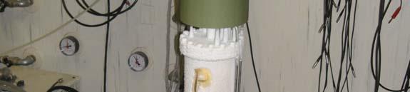
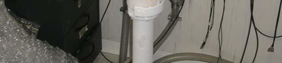
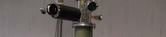
23 LT-AFM system for SGM
 With vibration and noise isolation system 3 He insert (300 mk) 9 T")
24 Customized cryogenic microscope System allows standard AFM and STM operation AFM non-optical detection scheme (tuning fork) With vibration and noise isolation system 3 He insert (300 mk) 9 T cryomagnet


25 Oct 2007: First cooldown


26 AFM Head Positioner (range in xyz > 6 mm) allow to locate features on the sample with µm precision Scan range: 42µm x 42µm x RT 8.5µm x 8.5µm x 300 mk Temperature measurement (RuO 2 ) close to sample Drift < 1 nm / h Temperature stability Delta T / T < 5% for hours, even at max. B field Noise in z at 300 mk: 1nm

27 Tuning Fork


28 AFM at room temperature


29 AFM at low temperature T = 350 mk B = 0 T B = 9 T


30 Sample holder for transport measurements Base mounted on AFM scanner Contact via pogo pins Chip carrier holds sample

31 Tip sample geometry
32 Sample temperature calibration Coulomb Blockade Thermometer (CBT) He 3 pot (RuOx): Close to sample (RuOx): Sample (CBT): 290 mk 365 mk 410 mk


33 STM Head High stability positioner Linear travel in xyz: 5 mm Step size K Max. speed 1 mm / s Piezo Tube Scanner Smaller scan range: 2 um in xy, 400 nm in z. Higher stability and resolution Temperature measurement (RuO 2 ) close to sample


34 320 mk, sample HOPG, tip PtIr B = 0 T B = 9 T 21/10/2007
35 Samples High-mobility AlGaAs heterostructures Depth d = 55 nm Electron density n = 3.37 x cm -2 Dark mobility μ = 2.62 x 10 6 cm 2 /V s Fermi wavelength λ F = 43 nm Mean free path L = 25 μm Schottky split-gate QPC Ti / Au bilayer (10 nm / 20 nm) Gap 300 nm

36 Hall-bar samples 1900 μm x 300 μm

37 Hall-bar samples

38 Hall-bar samples


39 Hall-bar samples
40 Hall-bar samples

41 Hall-bar samples 3 rd plateau
42 QPC at 3 rd plateau G = 6 e 2 /h nm 0.00 G = 0
43 QPC at 2 nd plateau G = 6 e 2 /h 5.50 G = 4 e 2 /h 600nm 0.00 G = 0
44 QPC at 1 st plateau G = 6 e 2 /h 5.50 G = 2 e 2 /h 600nm 0.00 G = 0


45 QPC at 3 rd plateau G = 6 e 2 /h nm 0.00 G = 0

46 QPC at 2 nd plateau 600nm
47 QPC at 1 st plateau 600nm
48 Branched flow of electrons No magnetic field (B = 0) QPC conductance G = 6 e 2 /h (3 rd plateau) Tip voltage V tip = -5 V, height h tip = 10 nm see also M. A. Topinka et al., Nature 410 (2001) 183.

49 Tip-induced backscattering

50 Branched flow of electrons No magnetic field (B = 0) QPC conductance G = 6 e 2 /h (3 rd plateau) Tip voltage V tip = -5 V, height h tip = 10 nm see also M. A. Topinka et al., Nature 410 (2001) 183.

51 Tip-induced backscattering


52 Interference fringes 400nm 100nm


53 Impact of small magnetic field G43: 0 mt G45: 5 mt 400nm 400nm

54 SGM in the Quantum Hall regime Tip voltage V tip = -5 V, height = 30 nm
55 Magnetoresistance


56 Selective control of edge channel trajectories by SGM Bulk filling factor ν=4 B = 3.04 T 2 spin-degenerate edge channels gate-region filling factors g 1 = g 2 = 0 600nm ee 2 /h 2 /h e 2 /h 0.0 e 2 /h
57 Determine the local filling factor v bulk = 4
58 Determine the local filling factor 0 v bulk = 4
 0 v bulk")
59 Determine the local filling factor Depleted (g = 0) 0 v bulk = 4 0
60 Determine the local filling factor Depleted (g = 0) 0 v bulk = 4 0 Sweep one gate
61 Determine the local filling factor Depleted (g = 0) 0 v bulk = 4 0 Sweep one gate
62 Determine the local filling factor Depleted (g = 0) 0 v bulk = 4 0 Sweep one gate
63 Asymmetrical gate bias 600nm g 1 = 0, g 2 = 2 Only inner edge channel can be backscattered Outer edge has no counterpart for backscattering G min = 2 e 2 /h
64 Asymmetrical gate bias 600nm 600nm


65 Identical filling factors g 1 = g 2 = 2 600nm 600nm 600nm


66 Edge state transmission for ν = 6 V tip = -3 V Bulk filling factor ν = 6 (3 spin-degenerate edge channels)
67 Summary Lower bound for conductance determined by number of paired edges Unpaired edge channels unaffected by tip gating Our results are a crucial first step for implementation of multi-edge beam mixers and interferometers
Quantum Hall circuits with variable geometry: study of the inter-channel equilibration by Scanning Gate Microscopy
 *nicola.paradiso@sns.it Nicola Paradiso Ph. D. Thesis Quantum Hall circuits with variable geometry: study of the inter-channel equilibration by Scanning Gate Microscopy N. Paradiso, Advisors: S. Heun,
Nanomaterials Characterization by lowtemperature Scanning Probe Microscopy
 Nanomaterials Characterization by lowtemperature Scanning Probe Microscopy Stefan Heun NEST, Istituto Nanoscienze-CNR and Scuola Normale Superiore Piazza San Silvestro 12, 56127 Pisa, Italy e-mail: stefan.heun@nano.cnr.it
What is Quantum Transport?
 What is Quantum Transport? Branislav K. Nikolić Department of Physics and Astronomy, University of Delaware, U.S.A. http://www.physics.udel.edu/~bnikolic Semiclassical Transport (is boring!) Bloch-Boltzmann
From nanophysics research labs to cell phones. Dr. András Halbritter Department of Physics associate professor
 From nanophysics research labs to cell phones Dr. András Halbritter Department of Physics associate professor Curriculum Vitae Birth: 1976. High-school graduation: 1994. Master degree: 1999. PhD: 2003.
2D Materials Research Activities at the NEST lab in Pisa, Italy. Stefan Heun NEST, Istituto Nanoscienze-CNR and Scuola Normale Superiore, Pisa, Italy
 2D Materials Research Activities at the NEST lab in Pisa, Italy Stefan Heun NEST, Istituto Nanoscienze-CNR and Scuola Normale Superiore, Pisa, Italy 2D Materials Research Activities at the NEST lab in
Nuclear spin spectroscopy for semiconductor hetero and nano structures
 (Interaction and Nanostructural Effects in Low-Dimensional Systems) November 16th, Kyoto, Japan Nuclear spin spectroscopy for semiconductor hetero and nano structures Yoshiro Hirayama Tohoku University
Scanning Gate Microscopy (SGM) of semiconductor nanostructures
 of semiconductor nanostructures") Scanning Gate Microscopy (SGM) of semiconductor nanostructures H. Sellier, P. Liu, B. Sacépé, S. Huant Dépt NANO, Institut NEEL, Grenoble, France B. Hackens, F. Martins, V. Bayot UCL, Louvain-la-Neuve,
Scanning Gate Microscopy (SGM) of semiconductor nanostructures H. Sellier, P. Liu, B. Sacépé, S. Huant Dépt NANO, Institut NEEL, Grenoble, France B. Hackens, F. Martins, V. Bayot UCL, Louvain-la-Neuve,
Charging and Kondo Effects in an Antidot in the Quantum Hall Regime
 Semiconductor Physics Group Cavendish Laboratory University of Cambridge Charging and Kondo Effects in an Antidot in the Quantum Hall Regime M. Kataoka C. J. B. Ford M. Y. Simmons D. A. Ritchie University
Electron Interferometer Formed with a Scanning Probe Tip and Quantum Point Contact Supplementary Information
 Electron Interferometer Formed with a Scanning Probe Tip and Quantum Point Contact Supplementary Information Section I: Experimental Details Here we elaborate on the experimental details described for
Low Vibration Cryogenic Equipment
 PAGE 12 PAGE 13 ATTOCUBE S CRYOSTATS ATTODRY attodry1000....................... 14 cryogen-free cryostats with/without s attodry700.........................18 cryogen-free table-top cryostats with optical
Quantized Resistance. Zhifan He, Huimin Yang Fudan University (China) April 9, Physics 141A
 April 9, Physics 141A") Quantized Resistance Zhifan He, Huimin Yang Fudan University (China) April 9, Physics 141A Outline General Resistance Hall Resistance Experiment of Quantum Hall Effect Theory of QHE Other Hall Effect General
Quantized Resistance Zhifan He, Huimin Yang Fudan University (China) April 9, Physics 141A Outline General Resistance Hall Resistance Experiment of Quantum Hall Effect Theory of QHE Other Hall Effect General
Electronic Quantum Transport in Mesoscopic Semiconductor Structures
 Thomas Ihn Electronic Quantum Transport in Mesoscopic Semiconductor Structures With 90 Illustrations, S in Full Color Springer Contents Part I Introduction to Electron Transport l Electrical conductance
Lectures: Condensed Matter II 1 Electronic Transport in Quantum dots 2 Kondo effect: Intro/theory. 3 Kondo effect in nanostructures
 Lectures: Condensed Matter II 1 Electronic Transport in Quantum dots 2 Kondo effect: Intro/theory. 3 Kondo effect in nanostructures Luis Dias UT/ORNL Lectures: Condensed Matter II 1 Electronic Transport
Correlated 2D Electron Aspects of the Quantum Hall Effect
 Correlated 2D Electron Aspects of the Quantum Hall Effect Magnetic field spectrum of the correlated 2D electron system: Electron interactions lead to a range of manifestations 10? = 4? = 2 Resistance (arb.
SUPPLEMENTARY INFORMATION
 Dirac electron states formed at the heterointerface between a topological insulator and a conventional semiconductor 1. Surface morphology of InP substrate and the device Figure S1(a) shows a 10-μm-square
Impact of disorder and topology in two dimensional systems at low carrier densities
 Impact of disorder and topology in two dimensional systems at low carrier densities A Thesis Submitted For the Degree of Doctor of Philosophy in the Faculty of Science by Mohammed Ali Aamir Department
The BTE with a High B-field
 ECE 656: Electronic Transport in Semiconductors Fall 2017 The BTE with a High B-field Mark Lundstrom Electrical and Computer Engineering Purdue University West Lafayette, IN USA 10/11/17 Outline 1) Introduction
Laughlin quasiparticle interferometer: Observation of Aharonov-Bohm superperiod and fractional statistics
 Laughlin quasiparticle interferometer: Observation of Aharonov-Bohm superperiod and fractional statistics F.E. Camino, W. Zhou and V.J. Goldman Stony Brook University Outline Exchange statistics in 2D,
Observation of topological surface state quantum Hall effect in an intrinsic three-dimensional topological insulator
 Observation of topological surface state quantum Hall effect in an intrinsic three-dimensional topological insulator Authors: Yang Xu 1,2, Ireneusz Miotkowski 1, Chang Liu 3,4, Jifa Tian 1,2, Hyoungdo
SiC Graphene Suitable For Quantum Hall Resistance Metrology.
 SiC Graphene Suitable For Quantum Hall Resistance Metrology. Samuel Lara-Avila 1, Alexei Kalaboukhov 1, Sara Paolillo, Mikael Syväjärvi 3, Rositza Yakimova 3, Vladimir Fal'ko 4, Alexander Tzalenchuk 5,
Final Research Report: Electronic and spin properties of one-dimensional semiconductor systems
 Final Research Report: Electronic and spin properties of one-dimensional semiconductor systems Researcher: Sébastien Faniel Advisor: Sorin Melinte 1. Initial objectives The purpose of our project was to
SUPPLEMENTARY INFORMATION
 doi:1.138/nature12186 S1. WANNIER DIAGRAM B 1 1 a φ/φ O 1/2 1/3 1/4 1/5 1 E φ/φ O n/n O 1 FIG. S1: Left is a cartoon image of an electron subjected to both a magnetic field, and a square periodic lattice.
Physics of Semiconductors
 Physics of Semiconductors 13 th 2016.7.11 Shingo Katsumoto Department of Physics and Institute for Solid State Physics University of Tokyo Outline today Laughlin s justification Spintronics Two current
Zooming in on the Quantum Hall Effect
 Zooming in on the Quantum Hall Effect Cristiane MORAIS SMITH Institute for Theoretical Physics, Utrecht University, The Netherlands Capri Spring School p.1/31 Experimental Motivation Historical Summary:
Electrical Standards based on quantum effects: Part II. Beat Jeckelmann
 Electrical Standards based on quantum effects: Part II Beat Jeckelmann Part II: The Quantum Hall Effect Overview Classical Hall effect Two-dimensional electron gas Landau levels Measurement technique Accuracy
Screening Model of Magnetotransport Hysteresis Observed in arxiv:cond-mat/ v1 [cond-mat.mes-hall] 27 Jul Bilayer Quantum Hall Systems
![Screening Model of Magnetotransport Hysteresis Observed in arxiv:cond-mat/ v1 [cond-mat.mes-hall] 27 Jul Bilayer Quantum Hall Systems](/thumbs/76/74053861.jpg "Screening Model of Magnetotransport Hysteresis Observed in arxiv:cond-mat/ v1 [cond-mat.mes-hall] 27 Jul Bilayer Quantum Hall Systems") , Screening Model of Magnetotransport Hysteresis Observed in arxiv:cond-mat/0607724v1 [cond-mat.mes-hall] 27 Jul 2006 Bilayer Quantum Hall Systems Afif Siddiki, Stefan Kraus, and Rolf R. Gerhardts Max-Planck-Institut
, Screening Model of Magnetotransport Hysteresis Observed in arxiv:cond-mat/0607724v1 [cond-mat.mes-hall] 27 Jul 2006 Bilayer Quantum Hall Systems Afif Siddiki, Stefan Kraus, and Rolf R. Gerhardts Max-Planck-Institut
Measurements of quasi-particle tunneling in the υ = 5/2 fractional. quantum Hall state
 Measurements of quasi-particle tunneling in the υ = 5/2 fractional quantum Hall state X. Lin, 1, * C. Dillard, 2 M. A. Kastner, 2 L. N. Pfeiffer, 3 and K. W. West 3 1 International Center for Quantum Materials,
arxiv:cond-mat/ v1 [cond-mat.mes-hall] 18 Jul 2000
![arxiv:cond-mat/ v1 [cond-mat.mes-hall] 18 Jul 2000](/thumbs/87/96520166.jpg "arxiv:cond-mat/ v1 [cond-mat.mes-hall] 18 Jul 2000") Topographic Mapping of the Quantum Hall Liquid using a Few-Electron Bubble G. Finkelstein, P.I. Glicofridis, R.C. Ashoori Department of Physics and Center for Materials Science and Engineering, Massachusetts
Topographic Mapping of the Quantum Hall Liquid using a Few-Electron Bubble G. Finkelstein, P.I. Glicofridis, R.C. Ashoori Department of Physics and Center for Materials Science and Engineering, Massachusetts
Dephasing of an Electronic Two-Path Interferometer
 Dephasing of an Electronic Two-Path Interferometer I. Gurman, R. Sabo, M. Heiblum, V. Umansky, and D. Mahalu Braun Center for Submicron Research, Dept. of Condensed Matter physics, Weizmann Institute of
FIG. 1: (Supplementary Figure 1: Large-field Hall data) (a) AHE (blue) and longitudinal
 (a) AHE (blue) and longitudinal") FIG. 1: (Supplementary Figure 1: Large-field Hall data) (a) AHE (blue) and longitudinal MR (red) of device A at T =2 K and V G - V G 0 = 100 V. Bold blue line is linear fit to large field Hall data (larger
FIG. 1: (Supplementary Figure 1: Large-field Hall data) (a) AHE (blue) and longitudinal MR (red) of device A at T =2 K and V G - V G 0 = 100 V. Bold blue line is linear fit to large field Hall data (larger
InAs/GaSb A New Quantum Spin Hall Insulator
 InAs/GaSb A New Quantum Spin Hall Insulator Rui-Rui Du Rice University 1. Old Material for New Physics 2. Quantized Edge Modes 3. Andreev Reflection 4. Summary KITP Workshop on Topological Insulator/Superconductor
Observation of neutral modes in the fractional quantum hall effect regime. Aveek Bid
 Observation of neutral modes in the fractional quantum hall effect regime Aveek Bid Department of Physics, Indian Institute of Science, Bangalore Nature 585 466 (2010) Quantum Hall Effect Magnetic field
Quantum Hall Effect in Vanishing Magnetic Fields
 Quantum Hall Effect in Vanishing Magnetic Fields Wei Pan Sandia National Labs Sandia is a multi-mission laboratory operated by Sandia Corporation, a Lockheed Martin Company, for the United States Department
Quantum Interference and Decoherence in Hexagonal Antidot Lattices
 Quantum Interference and Decoherence in Hexagonal Antidot Lattices Yasuhiro Iye, Masaaki Ueki, Akira Endo and Shingo Katsumoto Institute for Solid State Physics, University of Tokyo, -1- Kashiwanoha, Kashiwa,
Réunion erc. Gwendal Fève. Panel PE3 12 mn presentation 12 mn questions
 Réunion erc Gwendal Fève Panel PE3 12 mn presentation 12 mn questions Electron quantum optics in quantum Hall edge channels Gwendal Fève Laboratoire Pierre Aigrain, Ecole Normale Supérieure-CNRS Professor
Quantum Condensed Matter Physics Lecture 17
 Quantum Condensed Matter Physics Lecture 17 David Ritchie http://www.sp.phy.cam.ac.uk/drp/home 17.1 QCMP Course Contents 1. Classical models for electrons in solids. Sommerfeld theory 3. From atoms to
Distinct Signatures for Coulomb Blockade and Aharonov-Bohm Interference in Electronic Fabry-Perot Interferometers
 Distinct Signatures for Coulomb lockade and Aharonov-ohm Interference in Electronic Fabry-Perot Interferometers The Harvard community has made this article openly available. Please share how this access
Lecture 20: Semiconductor Structures Kittel Ch 17, p , extra material in the class notes
 Lecture 20: Semiconductor Structures Kittel Ch 17, p 494-503, 507-511 + extra material in the class notes MOS Structure Layer Structure metal Oxide insulator Semiconductor Semiconductor Large-gap Semiconductor
Beyond the Quantum Hall Effect
 Beyond the Quantum Hall Effect Jim Eisenstein California Institute of Technology School on Low Dimensional Nanoscopic Systems Harish-chandra Research Institute January February 2008 Outline of the Lectures
Landau quantization, Localization, and Insulator-quantum. Hall Transition at Low Magnetic Fields
 Landau quantization, Localization, and Insulator-quantum Hall Transition at Low Magnetic Fields Tsai-Yu Huang a, C.-T. Liang a, Gil-Ho Kim b, C.F. Huang c, C.P. Huang a and D.A. Ritchie d a Department
Unconventional electron quantum optics in condensed matter systems
 Unconventional electron quantum optics in condensed matter systems Dario Ferraro Centre de Physique Théorique, Marseille nanoqt-2016, Kyiv, October 10, 2016 In collaboration with: J. Rech, T. Jonckheere,
2D Electron Systems: Magneto-Transport Quantum Hall Effects
 Hauptseminar: Advanced Physics of Nanosystems 2D Electron Systems: Magneto-Transport Quantum Hall Effects Steffen Sedlak The Hall Effect P.Y. Yu,, M.Cardona, Fundamentals of Semiconductors, Springer Verlag,
Quantum Hall Effect in Graphene p-n Junctions
 Quantum Hall Effect in Graphene p-n Junctions Dima Abanin (MIT) Collaboration: Leonid Levitov, Patrick Lee, Harvard and Columbia groups UIUC January 14, 2008 Electron transport in graphene monolayer New
QUANTUM INTERFERENCE IN SEMICONDUCTOR RINGS
 QUANTUM INTERFERENCE IN SEMICONDUCTOR RINGS PhD theses Orsolya Kálmán Supervisors: Dr. Mihály Benedict Dr. Péter Földi University of Szeged Faculty of Science and Informatics Doctoral School in Physics
Instrumentation and Operation
 Instrumentation and Operation 1 STM Instrumentation COMPONENTS sharp metal tip scanning system and control electronics feedback electronics (keeps tunneling current constant) image processing system data
Solid Surfaces, Interfaces and Thin Films
 Hans Lüth Solid Surfaces, Interfaces and Thin Films Fifth Edition With 427 Figures.2e Springer Contents 1 Surface and Interface Physics: Its Definition and Importance... 1 Panel I: Ultrahigh Vacuum (UHV)
Semiconductor Nanowires. Stefan Heun NEST, Istituto Nanoscienze-CNR and Scuola Normale Superiore, Pisa, Italy
 Semiconductor Nanowires Stefan Heun NEST, Istituto Nanoscienze-CNR and Scuola Normale Superiore, Pisa, Italy Leaning Tower in Pisa Pisa and Hangzhou: Twin towns since 2008 Institute of Nanoscience- National
File name: Supplementary Information Description: Supplementary Figures and Supplementary References. File name: Peer Review File Description:
 File name: Supplementary Information Description: Supplementary Figures and Supplementary References File name: Peer Review File Description: Supplementary Figure Electron micrographs and ballistic transport
Coulomb Drag in Graphene
 Graphene 2017 Coulomb Drag in Graphene -Toward Exciton Condensation Philip Kim Department of Physics, Harvard University Coulomb Drag Drag Resistance: R D = V 2 / I 1 Onsager Reciprocity V 2 (B)/ I 1 =
Topology and Fractionalization in 2D Electron Systems
 Lectures on Mesoscopic Physics and Quantum Transport, June 1, 018 Topology and Fractionalization in D Electron Systems Xin Wan Zhejiang University xinwan@zju.edu.cn Outline Two-dimensional Electron Systems
Quantum Wires and Quantum Point Contacts. Quantum conductance
 Quantum Wires and Quantum Point Contacts Quantum conductance Classification of quasi-1d systems 1. What is quantum of resistance in magnetic and transport measurements of nanostructures? Are these quanta
Conductance quantization and quantum Hall effect
 UNIVERSITY OF LJUBLJANA FACULTY OF MATHEMATICS AND PHYSICS DEPARTMENT FOR PHYSICS Miha Nemevšek Conductance quantization and quantum Hall effect Seminar ADVISER: Professor Anton Ramšak Ljubljana, 2004
Lecture 20 - Semiconductor Structures
 Lecture 0: Structures Kittel Ch 17, p 494-503, 507-511 + extra material in the class notes MOS Structure metal Layer Structure Physics 460 F 006 Lect 0 1 Outline What is a semiconductor Structure? Created
Lecture 4 Scanning Probe Microscopy (SPM)
") Lecture 4 Scanning Probe Microscopy (SPM) General components of SPM; Tip --- the probe; Cantilever --- the indicator of the tip; Tip-sample interaction --- the feedback system; Scanner --- piezoelectric
Lecture 4 Scanning Probe Microscopy (SPM) General components of SPM; Tip --- the probe; Cantilever --- the indicator of the tip; Tip-sample interaction --- the feedback system; Scanner --- piezoelectric
Graphene. Tianyu Ye November 30th, 2011
 Graphene Tianyu Ye November 30th, 2011 Outline What is graphene? How to make graphene? (Exfoliation, Epitaxial, CVD) Is it graphene? (Identification methods) Transport properties; Other properties; Applications;
What is a topological insulator? Ming-Che Chang Dept of Physics, NTNU
 What is a topological insulator? Ming-Che Chang Dept of Physics, NTNU A mini course on topology extrinsic curvature K vs intrinsic (Gaussian) curvature G K 0 G 0 G>0 G=0 K 0 G=0 G
The Physics of Nanoelectronics
 The Physics of Nanoelectronics Transport and Fluctuation Phenomena at Low Temperatures Tero T. Heikkilä Low Temperature Laboratory, Aalto University, Finland OXFORD UNIVERSITY PRESS Contents List of symbols
tunneling theory of few interacting atoms in a trap
 tunneling theory of few interacting atoms in a trap Massimo Rontani CNR-NANO Research Center S3, Modena, Italy www.nano.cnr.it Pino D Amico, Andrea Secchi, Elisa Molinari G. Maruccio, M. Janson, C. Meyer,
672 Advanced Solid State Physics. Scanning Tunneling Microscopy
 672 Advanced Solid State Physics Scanning Tunneling Microscopy Biao Hu Outline: 1. Introduction to STM 2. STM principle & working modes 3. STM application & extension 4. STM in our group 1. Introduction
Coherent Electron Focussing in a Two-Dimensional Electron Gas.
 EUROPHYSICSLETTERS 15 April 1988 Europhys. Lett., 5 (8), pp. 721-725 (1988) Coherent Electron Focussing in a Two-Dimensional Electron Gas. H. VANHOUTEN(*),B. J. VANWEES(**), J. E. MOOIJ(**),C. W. J. BEENAKKER(*)
Magnetotransport of Topological Insulators: Bismuth Selenide and Bismuth Telluride
 Magnetotransport of Topological Insulators: Bismuth Selenide and Bismuth Telluride Justin Kelly 2011 NSF/REU Program Physics Department, University of Notre Dame Advisors: Prof. Malgorzata Dobrowolska,
Les états de bord d un. isolant de Hall atomique
 Les états de bord d un isolant de Hall atomique séminaire Atomes Froids 2/9/22 Nathan Goldman (ULB), Jérôme Beugnon and Fabrice Gerbier Outline Quantum Hall effect : bulk Landau levels and edge states
Topological insulator part I: Phenomena
 Phys60.nb 5 Topological insulator part I: Phenomena (Part II and Part III discusses how to understand a topological insluator based band-structure theory and gauge theory) (Part IV discusses more complicated
Classification of Solids
 Classification of Solids Classification by conductivity, which is related to the band structure: (Filled bands are shown dark; D(E) = Density of states) Class Electron Density Density of States D(E) Examples
Magnetoresistance in a High Mobility Two- Dimensional Electron System as a Function of Sample Geometry
 Journal of Physics: Conference Series OPEN ACCESS Magnetoresistance in a High Mobility Two- Dimensional Electron System as a Function of Sample Geometry To cite this article: L Bockhorn et al 213 J. Phys.:
Experimental Reconstruction of the Berry Curvature in a Floquet Bloch Band
 Experimental Reconstruction of the Berry Curvature in a Floquet Bloch Band Christof Weitenberg with: Nick Fläschner, Benno Rem, Matthias Tarnowski, Dominik Vogel, Dirk-Sören Lühmann, Klaus Sengstock Rice
Intrinsic Electronic Transport Properties of High. Information
 Intrinsic Electronic Transport Properties of High Quality and MoS 2 : Supporting Information Britton W. H. Baugher, Hugh O. H. Churchill, Yafang Yang, and Pablo Jarillo-Herrero Department of Physics, Massachusetts
Coherence and Correlations in Transport through Quantum Dots
 Coherence and Correlations in Transport through Quantum Dots Rolf J. Haug Abteilung Nanostrukturen Institut für Festkörperphysik and Laboratory for Nano and Quantum Engineering Gottfried Wilhelm Leibniz
The Moore-Read Quantum Hall State: An Overview
 The Moore-Read Quantum Hall State: An Overview Nigel Cooper (Cambridge) [Thanks to Ady Stern (Weizmann)] Outline: 1. Basic concepts of quantum Hall systems 2. Non-abelian exchange statistics 3. The Moore-Read
Broken Symmetry States and Divergent Resistance in Suspended Bilayer Graphene
 Broken Symmetry States and Divergent Resistance in Suspended Bilayer Graphene The Harvard community has made this article openly available. Please share how this access benefits you. Your story matters.
Semiclassical formulation
 The story so far: Transport coefficients relate current densities and electric fields (currents and voltages). Can define differential transport coefficients + mobility. Drude picture: treat electrons
Carbon based Nanoscale Electronics
 Carbon based Nanoscale Electronics 09 02 200802 2008 ME class Outline driving force for the carbon nanomaterial electronic properties of fullerene exploration of electronic carbon nanotube gold rush of
 Original citation: Oswald, Josef and Roemer, Rudolf A.. (15) Imaging of condensed quantum states in the quantum hall effect regime. Physics Procedia, 75. pp. 314-325. 1.116/j.phpro.15.12.38 Permanent WRAP
Correlated 2D Electron Aspects of the Quantum Hall Effect
 Correlated 2D Electron Aspects of the Quantum Hall Effect Outline: I. Introduction: materials, transport, Hall effects II. III. IV. Composite particles FQHE, statistical transformations Quasiparticle charge
Topological insulators
 http://www.physik.uni-regensburg.de/forschung/fabian Topological insulators Jaroslav Fabian Institute for Theoretical Physics University of Regensburg Stara Lesna, 21.8.212 DFG SFB 689 what are topological
Graphite, graphene and relativistic electrons
 Graphite, graphene and relativistic electrons Introduction Physics of E. graphene Y. Andrei Experiments Rutgers University Transport electric field effect Quantum Hall Effect chiral fermions STM Dirac
Probing Wigner Crystals in the 2DEG using Microwaves
 Probing Wigner Crystals in the 2DEG using Microwaves G. Steele CMX Journal Club Talk 9 September 2003 Based on work from the groups of: L. W. Engel (NHMFL), D. C. Tsui (Princeton), and collaborators. CMX
Toward the microscopic understanding of conductance on a quantum mechanical basis
 2 Toward the microscopic understanding of conductance on a quantum mechanical basis 2.1 Quantum transport in metals When Lew Dawydowitsch Landau 1 published his paper on the diamagnetism of metals [16],
Physics of Low-Dimensional Semiconductor Structures
 Physics of Low-Dimensional Semiconductor Structures Edited by Paul Butcher University of Warwick Coventry, England Norman H. March University of Oxford Oxford, England and Mario P. Tosi Scuola Normale
arxiv: v1 [cond-mat.mes-hall] 15 Mar 2010
![arxiv: v1 [cond-mat.mes-hall] 15 Mar 2010](/thumbs/92/109859238.jpg "arxiv: v1 [cond-mat.mes-hall] 15 Mar 2010") Quantum phases: years of the Aharonov-Bohm Effect and years of the Berry phase arxiv:.8v [cond-mat.mes-hall] Mar Inferring the transport properties of edge-states formed at quantum Hall based Aharonov-Bohm
Quantum phases: years of the Aharonov-Bohm Effect and years of the Berry phase arxiv:.8v [cond-mat.mes-hall] Mar Inferring the transport properties of edge-states formed at quantum Hall based Aharonov-Bohm
Hydrogenated Graphene
 Hydrogenated Graphene Stefan Heun NEST, Istituto Nanoscienze-CNR and Scuola Normale Superiore Pisa, Italy Outline Epitaxial Graphene Hydrogen Chemisorbed on Graphene Hydrogen-Intercalated Graphene Outline
Quantum Hall Effect. Jessica Geisenhoff. December 6, 2017
 Quantum Hall Effect Jessica Geisenhoff December 6, 2017 Introduction In 1879 Edwin Hall discovered the classical Hall effect, and a hundred years after that came the quantum Hall effect. First, the integer
Scanning Probe Microscopy
 1 Scanning Probe Microscopy Dr. Benjamin Dwir Laboratory of Physics of Nanostructures (LPN) Benjamin.dwir@epfl.ch PH.D3.344 Outline: Introduction: What is SPM, history STM AFM Image treatment Advanced
Intrinsic Charge Fluctuations and Nuclear Spin Order in GaAs Nanostructures
 Physics Department, University of Basel Intrinsic Charge Fluctuations and Nuclear Spin Order in GaAs Nanostructures Dominik Zumbühl Department of Physics, University of Basel Basel QC2 Center and Swiss
Compositional mapping of semiconductor quantum dots by X-ray photoemission electron microscopy
 Compositional mapping of semiconductor quantum dots by X-ray photoemission electron microscopy Stefan Heun CNR-INFM, Italy, Laboratorio Nazionale TASC, Trieste and NEST-SNS, Pisa Outline A brief introduction
High-mobility electron transport on cylindrical surfaces
 High-mobility electron transport on cylindrical surfaces Klaus-Jürgen Friedland Paul-Drude-nstitute for Solid State Electronics, Berlin, Germany Concept to create high mobility electron gases on free standing
Quantum Electrodynamics in Graphene
 Quantum Electrodynamics in Graphene Judy G. Cherian Kutztown University of PA Physics REU 2006 Univ. Of Washington Advisor- Dr. David Cobden Dr. Sam Fain Andrew Jones Graphene, a single layer of graphite,
A BIT OF MATERIALS SCIENCE THEN PHYSICS
 GRAPHENE AND OTHER D ATOMIC CRYSTALS Andre Geim with many thanks to K. Novoselov, S. Morozov, D. Jiang, F. Schedin, I. Grigorieva, J. Meyer, M. Katsnelson A BIT OF MATERIALS SCIENCE THEN PHYSICS CARBON
Introduction to semiconductor nanostructures. Peter Kratzer Modern Concepts in Theoretical Physics: Part II Lecture Notes
 Introduction to semiconductor nanostructures Peter Kratzer Modern Concepts in Theoretical Physics: Part II Lecture Notes What is a semiconductor? The Fermi level (chemical potential of the electrons) falls
SUPPLEMENTARY INFORMATION
 DOI: 1.138/NMAT3449 Topological crystalline insulator states in Pb 1 x Sn x Se Content S1 Crystal growth, structural and chemical characterization. S2 Angle-resolved photoemission measurements at various
Suddards, Matthew Edmund (2007) Scanning Capacitance Microscopy in the Quantum Hall Regime. PhD thesis, University of Nottingham.
 Scanning Capacitance Microscopy in the Quantum Hall Regime. PhD thesis, University of Nottingham.") Suddards, Matthew Edmund (2007) Scanning Capacitance Microscopy in the Quantum Hall Regime. PhD thesis, University of Nottingham. Access from the University of Nottingham repository: http://eprints.nottingham.ac.uk/10356/1/thesis_final.pdf
Suddards, Matthew Edmund (2007) Scanning Capacitance Microscopy in the Quantum Hall Regime. PhD thesis, University of Nottingham. Access from the University of Nottingham repository: http://eprints.nottingham.ac.uk/10356/1/thesis_final.pdf
Interferometric and noise signatures of Majorana fermion edge states in transport experiments
 Interferometric and noise signatures of ajorana fermion edge states in transport experiments Grégory Strübi, Wolfgang Belzig, ahn-soo Choi, and C. Bruder Department of Physics, University of Basel, CH-056
Quantum physics in quantum dots
 Quantum physics in quantum dots Klaus Ensslin Solid State Physics Zürich AFM nanolithography Multi-terminal tunneling Rings and dots Time-resolved charge detection Moore s Law Transistors per chip 10 9
METAL/CARBON-NANOTUBE INTERFACE EFFECT ON ELECTRONIC TRANSPORT
 METAL/CARBON-NANOTUBE INTERFACE EFFECT ON ELECTRONIC TRANSPORT S. Krompiewski Institute of Molecular Physics, Polish Academy of Sciences, M. Smoluchowskiego 17, 60-179 Poznań, Poland OUTLINE 1. Introductory
Single Electron Transistor (SET)
") Single Electron Transistor (SET) SET: e - e - dot A single electron transistor is similar to a normal transistor (below), except 1) the channel is replaced by a small dot. C g 2) the dot is separated from
Single Electron Transistor (SET) SET: e - e - dot A single electron transistor is similar to a normal transistor (below), except 1) the channel is replaced by a small dot. C g 2) the dot is separated from
Towards nano-mri in mesoscopic transport systems
 Towards nano-mri in mesoscopic transport systems P. Peddibhotla, M. Montinaro, D. Weber, F. Xue, and M. Poggio Swiss Nanoscience Institute Department of Physics University of Basel Switzerland 3 rd Nano-MRI
arxiv:cond-mat/ v1 17 Jan 1996
 Ballistic Composite Fermions in Semiconductor Nanostructures J. E. F. Frost, C.-T. Liang, D. R. Mace, M. Y. Simmons, D. A. Ritchie and M. Pepper Cavendish Laboratory, Madingley Road, Cambridge CB3 0HE,
Lecture 2 2D Electrons in Excited Landau Levels
 Lecture 2 2D Electrons in Excited Landau Levels What is the Ground State of an Electron Gas? lower density Wigner Two Dimensional Electrons at High Magnetic Fields E Landau levels N=2 N=1 N= Hartree-Fock
GRAPHENE the first 2D crystal lattice
 GRAPHENE the first 2D crystal lattice dimensionality of carbon diamond, graphite GRAPHENE realized in 2004 (Novoselov, Science 306, 2004) carbon nanotubes fullerenes, buckyballs what s so special about
Low Temperature Physics Measurement Systems
 PAGE 6 & 2008 2007 PRODUCT CATALOG Accelerate your Semiconductor Research & Developments towards Nanoscale Products. Experience your new working horse in the emerging field of semiconductor research for