GRAPHENE the first 2D crystal lattice
|
|
|
- Barnard Chase
- 5 years ago
- Views:
Transcription


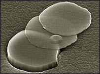
1 GRAPHENE the first 2D crystal lattice


2 dimensionality of carbon diamond, graphite GRAPHENE realized in 2004 (Novoselov, Science 306, 2004) carbon nanotubes fullerenes, buckyballs


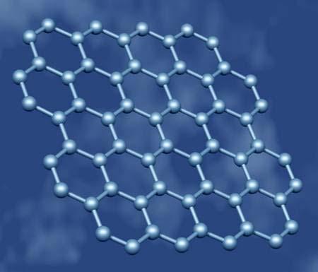
3 what s so special about graphene? crystal honeycomb symmetry with two sublattices A and B - two atoms per unit cell - two conical points per Brillouin zone - band crossing at K and K -linear low-energy dispersion E = hv F k fermi velocity v F = 10 6 m -1 s -1
4 relativistic, massless Dirac fermions linear dispersion at the Dirac-point effective mass m* = 0 description rather with Dirac instead of Schrödinger equation: this is a spinor wavefunction in QED where the pseudospin σ indicates the sublattices A and B the projection of the pseudospin on the k-direction gives rise to a new internal degree of freedom: chirality many features of graphene are understood as conservation of chirality and pseudospin σ

5 graphene on Si/SiO 2 substrate etched into a Hall-bar structure charge transport in graphene resistance conductance universal quantum conductance minimum?

6 half-integer QHE graphene: half-integer QHE no plateau at zero energy Landau levels in the density of states bilayer graphene: integer QHE but N=0 plateau missing!


7 Klein paradox tunneling of relativistic particels through potential barriers with T =1 -barrier repulsive for electrons -but attractive for positrons magic angles for single and bilayer graphene therefore electrostatic definition of devices with metal gates is not possible!


8 mechanical cleavage peeling off layers of graphite with a sticky tape transfer onto substrate optical microscope image of resulting flakes


9 further steps - localisation of appropriate flakes with optical microscope - contacting with metal electrodes by e-beam lithographie -writing an etch-mask with e-beam lithographie - reactive ion etching with Ar/O 2 plasma - wire-bonding to contact pins and testing the device - further etching, if necessary to narrow the graphene structures


10 submicron device conductance measurements of a 250 nm graphene quantum T = 4K; typical V-shape with fluctuations inset: - CB oscillations in the low-conductance region - Coulomb diamonds E c = 3 mev periodic CB resonances of the same T= 0.3K V g = 16 mev

11 intermediate quantum dot CB peaks and Coulomb diamonds of a 40 nm graphene T = 4K; irregular spacing and height excited states are hardly visible at V b =10 mev δe = 10meV E = E c +δe large V g variation indicates the confinement energy beeing larger than E c due to δe = α/d for massless quasiparticels α = ev nm
12 chaotic Dirac billiards peak spacing histograms for different D: random position for D < 100 nm Dirac fermions confined to a ideal disk Poisson distribution of E observed: Gaussian unitary ensemble quantum chaos in Dirac billiards δe ~ 1/D 2 at relatively large diameters


13 quantum confinement dot D < 30 nm quantum confinement dominating levelspacing up to 50 mev excited states visible due to extremely narrow constrictions defining the quantum dots
14 room temperature graphene FET transistor action of ~ 1nm constriction device at room temperature level spacing: ~ 0.5 ev
15 large gaps for narrow constrictions quantum point contacts mesoscopic fluctuations in conductance QPC transparencies limit the CB region of the quantum dots
16 CONCLUSION graphene is a great material there s a lot of work to be done Thank You!
Quantum Confinement in Graphene
 Quantum Confinement in Graphene from quasi-localization to chaotic billards MMM dominikus kölbl 13.10.08 1 / 27 Outline some facts about graphene quasibound states in graphene numerical calculation of
Carbon based Nanoscale Electronics
 Carbon based Nanoscale Electronics 09 02 200802 2008 ME class Outline driving force for the carbon nanomaterial electronic properties of fullerene exploration of electronic carbon nanotube gold rush of
Graphite, graphene and relativistic electrons
 Graphite, graphene and relativistic electrons Introduction Physics of E. graphene Y. Andrei Experiments Rutgers University Transport electric field effect Quantum Hall Effect chiral fermions STM Dirac
Supporting Online Material for
 www.sciencemag.org/cgi/content/full/320/5874/356/dc1 Supporting Online Material for Chaotic Dirac Billiard in Graphene Quantum Dots L. A. Ponomarenko, F. Schedin, M. I. Katsnelson, R. Yang, E. W. Hill,
Graphene - most two-dimensional system imaginable
 Graphene - most two-dimensional system imaginable A suspended sheet of pure graphene a plane layer of C atoms bonded together in a honeycomb lattice is the most two-dimensional system imaginable. A.J.
Graphene. Tianyu Ye November 30th, 2011
 Graphene Tianyu Ye November 30th, 2011 Outline What is graphene? How to make graphene? (Exfoliation, Epitaxial, CVD) Is it graphene? (Identification methods) Transport properties; Other properties; Applications;
3-month progress Report
 3-month progress Report Graphene Devices and Circuits Supervisor Dr. P.A Childs Table of Content Abstract... 1 1. Introduction... 1 1.1 Graphene gold rush... 1 1.2 Properties of graphene... 3 1.3 Semiconductor
Graphene The Search For Two Dimensions. Christopher Scott Friedline Arizona State University
 Graphene The Search For Two Dimensions Christopher Scott Friedline Arizona State University What Is Graphene? Single atomic layer of graphite arranged in a honeycomb crystal lattice Consists of sp 2 -bonded
Graphene A One-Atom-Thick Material for Microwave Devices
 ROMANIAN JOURNAL OF INFORMATION SCIENCE AND TECHNOLOGY Volume 11, Number 1, 2008, 29 35 Graphene A One-Atom-Thick Material for Microwave Devices D. DRAGOMAN 1, M. DRAGOMAN 2, A. A. MÜLLER3 1 University
EN2912C: Future Directions in Computing Lecture 08: Overview of Near-Term Emerging Computing Technologies
 EN2912C: Future Directions in Computing Lecture 08: Overview of Near-Term Emerging Computing Technologies Prof. Sherief Reda Division of Engineering Brown University Fall 2008 1 Near-term emerging computing
Overview. Carbon in all its forms. Background & Discovery Fabrication. Important properties. Summary & References. Overview of current research
 Graphene Prepared for Solid State Physics II Pr Dagotto Spring 2009 Laurene Tetard 03/23/09 Overview Carbon in all its forms Background & Discovery Fabrication Important properties Overview of current
Theories of graphene. Reinhold Egger Heinrich-Heine-Universität Düsseldorf Kolloquium, Hamburg
 Theories of graphene Reinhold Egger Heinrich-Heine-Universität Düsseldorf Kolloquium, Hamburg 1. 5. 011 Graphene monolayer Mother of all-carbon materials (fullerenes, nanotubes, graphite): made of benzene
Graphene transistor. Seminar I a. Mentor: doc. dr. Tomaž Rejec. April Abstract
 Graphene transistor Seminar I a Jan Srpčič Mentor: doc. dr. Tomaž Rejec April 2015 Abstract The topic of this seminar is graphene and its possible applications in the field of electronics, most notably
Transient Photocurrent Measurements of Graphene Related Materials
 Transient Photocurrent Measurements of Graphene Related Materials P. Srinivasa Rao Mentor: Prof. dr. Gvido Bratina Laboratory of Organic Matter Physics University of Nova Gorica 1 Contents: 1. Electrical
Nanoscience, MCC026 2nd quarter, fall Quantum Transport, Lecture 1/2. Tomas Löfwander Applied Quantum Physics Lab
 Nanoscience, MCC026 2nd quarter, fall 2012 Quantum Transport, Lecture 1/2 Tomas Löfwander Applied Quantum Physics Lab Quantum Transport Nanoscience: Quantum transport: control and making of useful things
SiC Graphene Suitable For Quantum Hall Resistance Metrology.
 SiC Graphene Suitable For Quantum Hall Resistance Metrology. Samuel Lara-Avila 1, Alexei Kalaboukhov 1, Sara Paolillo, Mikael Syväjärvi 3, Rositza Yakimova 3, Vladimir Fal'ko 4, Alexander Tzalenchuk 5,
A BIT OF MATERIALS SCIENCE THEN PHYSICS
 GRAPHENE AND OTHER D ATOMIC CRYSTALS Andre Geim with many thanks to K. Novoselov, S. Morozov, D. Jiang, F. Schedin, I. Grigorieva, J. Meyer, M. Katsnelson A BIT OF MATERIALS SCIENCE THEN PHYSICS CARBON
Transport through Andreev Bound States in a Superconductor-Quantum Dot-Graphene System
 Transport through Andreev Bound States in a Superconductor-Quantum Dot-Graphene System Nadya Mason Travis Dirk, Yung-Fu Chen, Cesar Chialvo Taylor Hughes, Siddhartha Lal, Bruno Uchoa Paul Goldbart University
Nanostructures. Lecture 13 OUTLINE
 Nanostructures MTX9100 Nanomaterials Lecture 13 OUTLINE -What is quantum confinement? - How can zero-dimensional materials be used? -What are one dimensional structures? -Why does graphene attract so much
TRANSVERSE SPIN TRANSPORT IN GRAPHENE
 International Journal of Modern Physics B Vol. 23, Nos. 12 & 13 (2009) 2641 2646 World Scientific Publishing Company TRANSVERSE SPIN TRANSPORT IN GRAPHENE TARIQ M. G. MOHIUDDIN, A. A. ZHUKOV, D. C. ELIAS,
Quantum Electrodynamics in Graphene
 Quantum Electrodynamics in Graphene Judy G. Cherian Kutztown University of PA Physics REU 2006 Univ. Of Washington Advisor- Dr. David Cobden Dr. Sam Fain Andrew Jones Graphene, a single layer of graphite,
Graphene: massless electrons in flatland.
 Graphene: massless electrons in flatland. Enrico Rossi Work supported by: University of Chile. Oct. 24th 2008 Collaorators CMTC, University of Maryland Sankar Das Sarma Shaffique Adam Euyuong Hwang Roman
Graphene and Quantum Hall (2+1)D Physics
D Physics") The 4 th QMMRC-IPCMS Winter School 8 Feb 2011, ECC, Seoul, Korea Outline 2 Graphene and Quantum Hall (2+1)D Physics Lecture 1. Electronic structures of graphene and bilayer graphene Lecture 2. Electrons
The 4 th QMMRC-IPCMS Winter School 8 Feb 2011, ECC, Seoul, Korea Outline 2 Graphene and Quantum Hall (2+1)D Physics Lecture 1. Electronic structures of graphene and bilayer graphene Lecture 2. Electrons
2-D Layered Materials 1
 2-D Layered Materials 1 Flatlands beyond Graphene Why the interest? 2D crystal with extraordinarily few defects Exotic electrical behaviors E = v F P (massless Dirac fermions) Efficient tunneling through
The many forms of carbon
 The many forms of carbon Carbon is not only the basis of life, it also provides an enormous variety of structures for nanotechnology. This versatility is connected to the ability of carbon to form two
Quantum transport through graphene nanostructures
 Quantum transport through graphene nanostructures S. Rotter, F. Libisch, L. Wirtz, C. Stampfer, F. Aigner, I. Březinová, and J. Burgdörfer Institute for Theoretical Physics/E136 December 9, 2009 Graphene
Beautiful Graphene, Photonic Crystals, Schrödinger and Dirac Billiards and Their Spectral Properties
 Beautiful Graphene, Photonic Crystals, Schrödinger and Dirac Billiards and Their Spectral Properties Cocoyoc 2012 Something about graphene and microwave billiards Dirac spectrum in a photonic crystal Experimental
Carbon nanotubes and Graphene
 16 October, 2008 Solid State Physics Seminar Main points 1 History and discovery of Graphene and Carbon nanotubes 2 Tight-binding approximation Dynamics of electrons near the Dirac-points 3 Properties
Electronic transport in low dimensional systems
 Electronic transport in low dimensional systems For example: 2D system l
Graphene and Carbon Nanotubes
 Graphene and Carbon Nanotubes 1 atom thick films of graphite atomic chicken wire Novoselov et al - Science 306, 666 (004) 100μm Geim s group at Manchester Novoselov et al - Nature 438, 197 (005) Kim-Stormer
Graphene FETs with Combined Structure and Transparent Top
 Available online at www.sciencedirect.com Physics Procedia 32 (2012 ) 869 874 18th International Vacuum Congress (IVC-18) Graphene FETs with Combined Structure and Transparent Top Yuanlin Yuan a, Zhen
Graphene: fundamentals
 Graphene: fundamentals François Peeters Condensed Matter Theory group Department of Physics University of Antwerp Email: francois.peeters@uantwerpen.be https://www.uantwerpen.be/en/rg/cmt/ Chemistry Graphitic
Lectures: Condensed Matter II 1 Electronic Transport in Quantum dots 2 Kondo effect: Intro/theory. 3 Kondo effect in nanostructures
 Lectures: Condensed Matter II 1 Electronic Transport in Quantum dots 2 Kondo effect: Intro/theory. 3 Kondo effect in nanostructures Luis Dias UT/ORNL Lectures: Condensed Matter II 1 Electronic Transport
SUPPLEMENTARY INFORMATION
 SUPPLEMENTARY INFORMATION DOI: 10.1038/NNANO.2011.138 Graphene Nanoribbons with Smooth Edges as Quantum Wires Xinran Wang, Yijian Ouyang, Liying Jiao, Hailiang Wang, Liming Xie, Justin Wu, Jing Guo, and
Electronic properties of graphene. Jean-Noël Fuchs Laboratoire de Physique des Solides Université Paris-Sud (Orsay)
") Electronic properties of graphene Jean-Noël Fuchs Laboratoire de Physique des Solides Université Paris-Sud (Orsay) Cargèse, September 2012 3 one-hour lectures in 2 x 1,5h on electronic properties of graphene
Electronic properties of graphene Jean-Noël Fuchs Laboratoire de Physique des Solides Université Paris-Sud (Orsay) Cargèse, September 2012 3 one-hour lectures in 2 x 1,5h on electronic properties of graphene
Final exam. Introduction to Nanotechnology. Name: Student number:
 1 Final exam. Introduction to Nanotechnology Name: Student number: 1. (a) What is the definition for a cluster size-wise? (3%) (b) Calculate the energy separation near the Fermi surface of a metallic cluster
Building blocks for nanodevices
 Building blocks for nanodevices Two-dimensional electron gas (2DEG) Quantum wires and quantum point contacts Electron phase coherence Single-Electron tunneling devices - Coulomb blockage Quantum dots (introduction)
Electronic properties of Graphene and 2-D materials
 Electronic properties of Graphene and 2-D materials 2D materials background Carbon allotropes Graphene Structure and Band structure Electronic properties Electrons in a magnetic field Onsager relation
arxiv:cond-mat/ v2 [cond-mat.mes-hall] 14 Aug 2006
![arxiv:cond-mat/ v2 [cond-mat.mes-hall] 14 Aug 2006](/thumbs/76/73692373.jpg "arxiv:cond-mat/ v2 [cond-mat.mes-hall] 14 Aug 2006") Chiral tunneling and the Klein paradox in graphene arxiv:cond-mat/0604323v2 [cond-mat.mes-hall] 14 Aug 2006 M. I. Katsnelson, 1 K. S. Novoselov, 2 and A. K. Geim 2 1 Institute for Molecules and Materials,
Chiral tunneling and the Klein paradox in graphene arxiv:cond-mat/0604323v2 [cond-mat.mes-hall] 14 Aug 2006 M. I. Katsnelson, 1 K. S. Novoselov, 2 and A. K. Geim 2 1 Institute for Molecules and Materials,
Broken Symmetry States and Divergent Resistance in Suspended Bilayer Graphene
 Broken Symmetry States and Divergent Resistance in Suspended Bilayer Graphene The Harvard community has made this article openly available. Please share how this access benefits you. Your story matters.
Initial Stages of Growth of Organic Semiconductors on Graphene
 Initial Stages of Growth of Organic Semiconductors on Graphene Presented by: Manisha Chhikara Supervisor: Prof. Dr. Gvido Bratina University of Nova Gorica Outline Introduction to Graphene Fabrication
Luttinger Liquid at the Edge of a Graphene Vacuum
 Luttinger Liquid at the Edge of a Graphene Vacuum H.A. Fertig, Indiana University Luis Brey, CSIC, Madrid I. Introduction: Graphene Edge States (Non-Interacting) II. III. Quantum Hall Ferromagnetism and
Single Electron Transistor (SET)
") Single Electron Transistor (SET) e - e - dot C g V g A single electron transistor is similar to a normal transistor (below), except 1) the channel is replaced by a small dot. 2) the dot is separated from
Single Electron Transistor (SET) e - e - dot C g V g A single electron transistor is similar to a normal transistor (below), except 1) the channel is replaced by a small dot. 2) the dot is separated from
The Physics of Nanoelectronics
 The Physics of Nanoelectronics Transport and Fluctuation Phenomena at Low Temperatures Tero T. Heikkilä Low Temperature Laboratory, Aalto University, Finland OXFORD UNIVERSITY PRESS Contents List of symbols
& Dirac Fermion confinement Zahra Khatibi
 Graphene & Dirac Fermion confinement Zahra Khatibi 1 Outline: What is so special about Graphene? applications What is Graphene? Structure Transport properties Dirac fermions confinement Necessity External
Impact of disorder and topology in two dimensional systems at low carrier densities
 Impact of disorder and topology in two dimensional systems at low carrier densities A Thesis Submitted For the Degree of Doctor of Philosophy in the Faculty of Science by Mohammed Ali Aamir Department
Black phosphorus: A new bandgap tuning knob
 Black phosphorus: A new bandgap tuning knob Rafael Roldán and Andres Castellanos-Gomez Modern electronics rely on devices whose functionality can be adjusted by the end-user with an external knob. A new
Graphene. L. Tetard 1,2. (Dated: April 7, 2009) 1 Oak Ridge National Laboratory, Oak Ridge, TN USA
 1 Oak Ridge National Laboratory, Oak Ridge, TN USA") Graphene L. Tetard 1,2 1 Oak Ridge National Laboratory, Oak Ridge, TN 37831-6123 USA 2 Department of Physics, University of Tennessee, Knoxville, TN 37996, USA (Dated: April 7, 2009) 1 Diamond, graphite,
Graphene L. Tetard 1,2 1 Oak Ridge National Laboratory, Oak Ridge, TN 37831-6123 USA 2 Department of Physics, University of Tennessee, Knoxville, TN 37996, USA (Dated: April 7, 2009) 1 Diamond, graphite,
Mesoscopic physics: From low-energy nuclear [1] to relativistic [2] high-energy analogies
![Mesoscopic physics: From low-energy nuclear [1] to relativistic [2] high-energy analogies](/thumbs/92/108493944.jpg "Mesoscopic physics: From low-energy nuclear [1] to relativistic [2] high-energy analogies") Mesoscopic physics: From low-energy nuclear [1] to relativistic [2] high-energy analogies Constantine Yannouleas and Uzi Landman School of Physics, Georgia Institute of Technology [1] Ch. 4 in Metal Clusters,
Mesoscopic physics: From low-energy nuclear [1] to relativistic [2] high-energy analogies Constantine Yannouleas and Uzi Landman School of Physics, Georgia Institute of Technology [1] Ch. 4 in Metal Clusters,
Electronic states on the surface of graphite
 Electronic states on the surface of graphite Guohong Li, Adina Luican, Eva Y. Andrei * Department of Physics and Astronomy, Rutgers Univsersity, Piscataway, NJ 08854, USA Elsevier use only: Received date
Graphene: carbon in two dimensions
 Graphene: carbon in two dimensions Carbon is one of the most intriguing elements in the Periodic Table. It forms many allotropes, some known from ancient times (diamond and graphite) and some discovered
Graphene FETs EE439 FINAL PROJECT. Yiwen Meng Su Ai
 Graphene FETs EE439 FINAL PROJECT Yiwen Meng Su Ai Introduction What is Graphene? An atomic-scale honeycomb lattice made of carbon atoms Before 2004, Hypothetical Carbon Structure Until 2004, physicists
Quantum dots. Quantum computing. What is QD. Invention QD TV. Complex. Lego. https://www.youtube.com/watch?v=ne819ppca5o
 Intel's New 49-qubit Quantum Chip & Neuromorphic Chip https://www.youtube.com/watch?v=ne819ppca5o How To Make a Quantum Bit https://www.youtube.com/watch?v=znzzggr2mhk Quantum computing https://www.youtube.com/watch?v=dxaxptlhqqq
Graphene: : CERN on the desk. Mikhail Katsnelson
 Graphene: : CERN on the desk Mikhail Katsnelson Instead of epigraph You can get much further with a kind word and a gun than you can with a kind word alone (Al Capone) You can get much further with an
Robustness of edge states in graphene quantum dots
 Chapter 5 Robustness of edge states in graphene quantum dots 5.1 Introduction The experimental discovery of graphene [3, 57], a monolayer of carbon atoms, has opened room for new electronic devices (for
Electronic Quantum Transport in Mesoscopic Semiconductor Structures
 Thomas Ihn Electronic Quantum Transport in Mesoscopic Semiconductor Structures With 90 Illustrations, S in Full Color Springer Contents Part I Introduction to Electron Transport l Electrical conductance
Physics and Material Science of Semiconductor Nanostructures
 Physics and Material Science of Semiconductor Nanostructures PHYS 570P Prof. Oana Malis Email: omalis@purdue.edu Course website: http://www.physics.purdue.edu/academic_programs/courses/phys570p/ 1 Introduction
Chapter 3 Properties of Nanostructures
 Chapter 3 Properties of Nanostructures In Chapter 2, the reduction of the extent of a solid in one or more dimensions was shown to lead to a dramatic alteration of the overall behavior of the solids. Generally,
Coulomb blockade behavior in nanostructured graphene with direct contacts
 Copyright 213 by American Scientific Publishers All rights reserved. Printed in the United States of America 2158-589/213/3/92/5 doi:1.1166/mex.213.115 www.aspbs.com/mex Coulomb blockade behavior in nanostructured
Introduction to Nanotechnology Chapter 5 Carbon Nanostructures Lecture 1
 Introduction to Nanotechnology Chapter 5 Carbon Nanostructures Lecture 1 ChiiDong Chen Institute of Physics, Academia Sinica chiidong@phys.sinica.edu.tw 02 27896766 Carbon contains 6 electrons: (1s) 2,
Graphene: Plane and Simple Electrical Metrology?
 Graphene: Plane and Simple Electrical Metrology? R. E. Elmquist, F. L. Hernandez-Marquez, M. Real, T. Shen, D. B. Newell, C. J. Jacob, and G. R. Jones, Jr. National Institute of Standards and Technology,
ELECTRONIC ENERGY DISPERSION AND STRUCTURAL PROPERTIES ON GRAPHENE AND CARBON NANOTUBES
 ELECTRONIC ENERGY DISPERSION AND STRUCTURAL PROPERTIES ON GRAPHENE AND CARBON NANOTUBES D. RACOLTA, C. ANDRONACHE, D. TODORAN, R. TODORAN Technical University of Cluj Napoca, North University Center of
Raman Imaging and Electronic Properties of Graphene
 Raman Imaging and Electronic Properties of Graphene F. Molitor, D. Graf, C. Stampfer, T. Ihn, and K. Ensslin Laboratory for Solid State Physics, ETH Zurich, 8093 Zurich, Switzerland ensslin@phys.ethz.ch
Graphene based FETs. Raghav Gupta ( )
") 1 Graphene based FETs Raghav Gupta (10327553) Abstract The extraordinary electronic properties along with excellent optical, mechanical, thermodynamic properties have led to a lot of interest in its possible
1 Graphene based FETs Raghav Gupta (10327553) Abstract The extraordinary electronic properties along with excellent optical, mechanical, thermodynamic properties have led to a lot of interest in its possible
Commensurability-dependent transport of a Wigner crystal in a nanoconstriction
 NPCQS2012, OIST Commensurability-dependent transport of a Wigner crystal in a nanoconstriction David Rees, RIKEN, Japan Kimitoshi Kono (RIKEN) Paul Leiderer (University of Konstanz) Hiroo Totsuji (Okayama
A. Optimizing the growth conditions of large-scale graphene films
 1 A. Optimizing the growth conditions of large-scale graphene films Figure S1. Optical microscope images of graphene films transferred on 300 nm SiO 2 /Si substrates. a, Images of the graphene films grown
Single Electron Transistor (SET)
") Single Electron Transistor (SET) SET: e - e - dot A single electron transistor is similar to a normal transistor (below), except 1) the channel is replaced by a small dot. C g 2) the dot is separated from
Single Electron Transistor (SET) SET: e - e - dot A single electron transistor is similar to a normal transistor (below), except 1) the channel is replaced by a small dot. C g 2) the dot is separated from
Graphene Novel Material for Nanoelectronics
 Graphene Novel Material for Nanoelectronics Shintaro Sato Naoki Harada Daiyu Kondo Mari Ohfuchi (Manuscript received May 12, 2009) Graphene is a flat monolayer of carbon atoms with a two-dimensional honeycomb
SUPPLEMENTARY INFORMATION
 Dirac cones reshaped by interaction effects in suspended graphene D. C. Elias et al #1. Experimental devices Graphene monolayers were obtained by micromechanical cleavage of graphite on top of an oxidized
No reason one cannot have double-well structures: With MBE growth, can control well thicknesses and spacings at atomic scale.
 The story so far: Can use semiconductor structures to confine free carriers electrons and holes. Can get away with writing Schroedinger-like equation for Bloch envelope function to understand, e.g., -confinement
Atomic collapse in graphene
 Atomic collapse in graphene Andrey V. Shytov (BNL) Work done in collaboration with: L.S. Levitov MIT M.I. Katsnelson University of Nijmegen, Netherlands * Phys. Rev. Lett. 99, 236801; ibid. 99, 246802
arxiv:cond-mat/ v1 [cond-mat.mes-hall] 20 Dec 2006
![arxiv:cond-mat/ v1 [cond-mat.mes-hall] 20 Dec 2006](/thumbs/80/81150486.jpg "arxiv:cond-mat/ v1 [cond-mat.mes-hall] 20 Dec 2006") Graphene: carbon in two dimensions arxiv:cond-mat/0612534v1 [cond-mat.mes-hall] 20 Dec 2006 Mikhail I. Katsnelson 1 1 Institute for Molecules and Materials, Radboud University Nijmegen, 6525 ED Nijmegen,
Graphene: carbon in two dimensions arxiv:cond-mat/0612534v1 [cond-mat.mes-hall] 20 Dec 2006 Mikhail I. Katsnelson 1 1 Institute for Molecules and Materials, Radboud University Nijmegen, 6525 ED Nijmegen,
Supplementary Figure S1. AFM images of GraNRs grown with standard growth process. Each of these pictures show GraNRs prepared independently,
 Supplementary Figure S1. AFM images of GraNRs grown with standard growth process. Each of these pictures show GraNRs prepared independently, suggesting that the results is reproducible. Supplementary Figure
Modeling and Performance analysis of Metallic CNT Interconnects for VLSI Applications
 IOSR Journal of Electronics and Communication Engineering (IOSR-JECE) e-issn: 2278-2834, p- ISSN: 2278-8735. Volume 4, Issue 6 (Jan. - Feb. 2013), PP 32-36 Modeling and Performance analysis of Metallic
Topological Phases under Strong Magnetic Fields
 Topological Phases under Strong Magnetic Fields Mark O. Goerbig ITAP, Turunç, July 2013 Historical Introduction What is the common point between graphene, quantum Hall effects and topological insulators?...
About OMICS Group Conferences
 About OMICS Group OMICS Group International is an amalgamation of Open Access publications and worldwide international science conferences and events. Established in the year 2007 with the sole aim of
Quantum Hall Effect in Graphene p-n Junctions
 Quantum Hall Effect in Graphene p-n Junctions Dima Abanin (MIT) Collaboration: Leonid Levitov, Patrick Lee, Harvard and Columbia groups UIUC January 14, 2008 Electron transport in graphene monolayer New
Gate-induced insulating state in bilayer graphene devices
 Gate-induced insulating state in bilayer graphene devices Jeroen B. Oostinga, Hubert B. Heersche, Xinglan Liu, Alberto F. Morpurgo and Lieven M. K. Vandersypen Kavli Institute of Nanoscience, Delft University
Electron Transport in Graphene-Based Double-Barrier Structure under a Time Periodic Field
 Commun. Theor. Phys. 56 (2011) 163 167 Vol. 56, No. 1, July 15, 2011 Electron Transport in Graphene-Based Double-Barrier Structure under a Time Periodic Field LU Wei-Tao ( å ) 1, and WANG Shun-Jin ( )
Spin orbit interaction in graphene monolayers & carbon nanotubes
 Spin orbit interaction in graphene monolayers & carbon nanotubes Reinhold Egger Institut für Theoretische Physik, Düsseldorf Alessandro De Martino Andreas Schulz, Artur Hütten MPI Dresden, 25.10.2011 Overview
From nanophysics research labs to cell phones. Dr. András Halbritter Department of Physics associate professor
 From nanophysics research labs to cell phones Dr. András Halbritter Department of Physics associate professor Curriculum Vitae Birth: 1976. High-school graduation: 1994. Master degree: 1999. PhD: 2003.
single-electron electron tunneling (SET)
") single-electron electron tunneling (SET) classical dots (SET islands): level spacing is NOT important; only the charging energy (=classical effect, many electrons on the island) quantum dots: : level spacing
single-electron electron tunneling (SET) classical dots (SET islands): level spacing is NOT important; only the charging energy (=classical effect, many electrons on the island) quantum dots: : level spacing
TRANSPORT MEASUREMENTS ON GRAPHENE P-N JUNCTIONS
 TRANSPORT MEASUREMENTS ON GRAPHENE P-N JUNCTIONS A DISSERTATION SUBMITTED TO THE DEPARTMENT OF PHYSICS AND THE COMMITTEE ON GRADUATE STUDIES OF STANFORD UNIVERSITY IN PARTIAL FULFILLMENT OF THE REQUIREMENTS
Conductance quantization and quantum Hall effect
 UNIVERSITY OF LJUBLJANA FACULTY OF MATHEMATICS AND PHYSICS DEPARTMENT FOR PHYSICS Miha Nemevšek Conductance quantization and quantum Hall effect Seminar ADVISER: Professor Anton Ramšak Ljubljana, 2004
Graphene electronics
 Graphene electronics Alberto Morpurgo Main collaborators J. Oostinga, H. Heersche, P. Jarillo Herrero, S. Russo, M. Craciun, L. Vandersypen, S. Tarucha, R. Danneau, P. Hakkonen A simple tight-binding H
Wafer-scale fabrication of graphene
 Wafer-scale fabrication of graphene Sten Vollebregt, MSc Delft University of Technology, Delft Institute of Mircosystems and Nanotechnology Delft University of Technology Challenge the future Delft University
Exceptional ballistic transport in epigraphene. Walt de Heer Georgia Institute of Technology
 Exceptional ballistic transport in epigraphene Walt de Heer Georgia Institute of Technology Program Objective First formulated in 2001 and patented in 2003, our objective is to develop nanoelectronics
SUPPLEMENTARY INFORMATION
 SUPPLEMENTARY INFORMATION SUPPLEMENTARY INFORMATION Trilayer graphene is a semimetal with a gate-tuneable band overlap M. F. Craciun, S. Russo, M. Yamamoto, J. B. Oostinga, A. F. Morpurgo and S. Tarucha
From an Experimental Test of the BGS Conjecture to Modeling Relativistic Effects in Microwave Billards
 From an Experimental Test of the BGS Conjecture to Modeling Relativistic Effects in Microwave Billards Oriol Bohigas Memorial Orsay 2014 Some personal recollections Some experimental tests of the BGS conjecture
Electronic properties of graphene
 phys. stat. sol. (b) 44, No. 11, 4106 4111 (007) / DOI 10.100/pssb.0077608 Electronic properties of graphene K. S. Novoselov *, 1, S. V. Morozov, T. M. G. Mohinddin 3, L. A. Ponomarenko 1, D. C. Elias
Classification of Solids
 Classification of Solids Classification by conductivity, which is related to the band structure: (Filled bands are shown dark; D(E) = Density of states) Class Electron Density Density of States D(E) Examples
Is Quantum Mechanics Chaotic? Steven Anlage
 Is Quantum Mechanics Chaotic? Steven Anlage Physics 40 0.5 Simple Chaos 1-Dimensional Iterated Maps The Logistic Map: x = 4 x (1 x ) n+ 1 μ n n Parameter: μ Initial condition: 0 = 0.5 μ 0.8 x 0 = 0.100
Modern Physics for Scientists and Engineers International Edition, 4th Edition
 Modern Physics for Scientists and Engineers International Edition, 4th Edition http://optics.hanyang.ac.kr/~shsong 1. THE BIRTH OF MODERN PHYSICS 2. SPECIAL THEORY OF RELATIVITY 3. THE EXPERIMENTAL BASIS
Relativistic Quantum Chaos
 Relativistic Quantum Chaos Liang Huang, 1 Hong-Ya Xu, 2 Celso Grebogi, 3, 4 2, 5, and Ying-Cheng Lai 1 School of Physical Science and Technology, and Key Laboratory for Magnetism and Magnetic Materials
Dirac fermions in Graphite:
 Igor Lukyanchuk Amiens University, France, Yakov Kopelevich University of Campinas, Brazil Dirac fermions in Graphite: I. Lukyanchuk, Y. Kopelevich et al. - Phys. Rev. Lett. 93, 166402 (2004) - Phys. Rev.
Quantum transport through graphene nanostructures
 Quantum transport through graphene nanostructures F. Libisch, S. Rotter, and J. Burgdörfer Institute for Theoretical Physics/E136, January 14, 2011 Graphene [1, 2], the rst true two-dimensional (2D) solid,
Surfaces, Interfaces, and Layered Devices
 Surfaces, Interfaces, and Layered Devices Building blocks for nanodevices! W. Pauli: God made solids, but surfaces were the work of Devil. Surfaces and Interfaces 1 Interface between a crystal and vacuum
Physical Properties of Mono-layer of
 Chapter 3 Physical Properties of Mono-layer of Silicene The fascinating physical properties[ 6] associated with graphene have motivated many researchers to search for new graphene-like two-dimensional
Suspended graphene: a bridge to the Dirac point.
 Suspended graphene: a bridge to the Dirac point. Xu Du, Ivan Skachko, Anthony Barker, Eva Y. Andrei Department of Physics & Astronomy, Rutgers the State University of New Jersey The recent discovery of
Metallic: 2n 1. +n 2. =3q Armchair structure always metallic = 2
 Properties of CNT d = 2.46 n 2 2 1 + n1n2 + n2 2π Metallic: 2n 1 +n 2 =3q Armchair structure always metallic a) Graphite Valence(π) and Conduction(π*) states touch at six points(fermi points) Carbon Nanotube: