About OMICS Group Conferences
|
|
|
- Dinah Shepherd
- 5 years ago
- Views:
Transcription
1 About OMICS Group OMICS Group International is an amalgamation of Open Access publications and worldwide international science conferences and events. Established in the year 2007 with the sole aim of making the information on Sciences and technology Open Access, OMICS Group publishes 400 online open access scholarly journals in all aspects of Science, Engineering, Management and Technology journals. OMICS Group has been instrumental in taking the knowledge on Science& technology to the doorsteps of ordinary men and women. Research Scholars, Students, Libraries, Educational Institutions, Research centers and the industry are main stakeholders that benefitted greatly from this knowledge dissemination. OMICS Group also organizes 300 International conferences annually across the globe, where knowledge transfer takes place through debates, round table discussions, poster presentations, workshops, symposia and exhibitions.
2 About OMICS Group Conferences OMICS Group International is a pioneer and leading science event organizer, which publishes around 400 open access journals and conducts over 300 Medical, Clinical, Engineering, Life Sciences, Phrama scientific conferences all over the globe annually with the support of more than 1000 scientific associations and 30,000 editorial board members and 3.5 million followers to its credit. OMICS Group has organized 500 conferences, workshops and national symposiums across the major cities including San Francisco, Las Vegas, San Antonio, Omaha, Orlando, Raleigh, Santa Clara, Chicago, Philadelphia, Baltimore, United Kingdom, Valencia, Dubai, Beijing, Hyderabad, Bengaluru and Mumbai.

467-2170, kyiv.phys.northwestern.")

3 and their applications Serhii Shafraniuk Physics & Astronomy Department, Northwestern University, Evanston IL Ph. (847) , kyiv.phys.northwestern.edu Experiment (GU): P. Barbara, M. Rinzan, Y. Yang Experiment (planned in NU): V. Chandrasekhar, I. Nevirkovets


4 Outline. Chirality and Klein paradox in graphene. Chemical, biological, d.c. magnetic, and electromagnetic sensors. Graphene and carbon nanotube quantum wells. Electron transport through the graphene and carbon nanotube junctions.
5 Graphene versus other AMM Graphene MS 2 Atomic monolayer M=Nb,Ta LS 2 Atomic monolayer L=Ti, Mo, W Advantages Intrinsic coherence due to chirality of electrons, Klein tunneling, Λ 10 3 W/(m K) and µ > 10 6 cm 2 /(V s) at 2 K Metal, superconductor, no dielectric gap ( = 0 ev) Λ W/(m K) Semiconductor with energy gap = 1 2 ev in the electron spectrum, Λ W/(m K) µ ~ 10 3 cm 2 /(V s) Setbacks No energy gap in electron spectrum of pristine graphene No intrinsic coherence No intrinsic coherence


6 Recent graphene applications Filter et al. Bahket al. THz graphene antenna Biotransferrable graphene wireless nanosensor, Princeton, NJ

7 Graphene s applications Intrinsic coherence A good durability Optical properties Chemical stability High speed transistors, single electron transistors, memory elements Electric and thermal wires Optical infrared and THz remote sensors and lasers Theremoelectric energy generators and coolers Chemical and biological sensors
8 Our activity at Northwestern Graphene and CNT quantum dots for THz electronics (jointly with Georgetown). Electron and heat transport through graphene/metal or CNT/metal interfaces (I. Nevirkovets). Graphene and carbon nanotube thermoelectric energy generators and coolers (T. Gupta, S. Davis, and V. Chandraseckar). Challenges Influence of surface (water molecules) and substrate defects. Forming of highly efficient local gates. Heat flow management. 8
9 Key aspects Chirality of low-energy excitations (regular spinless quasiparticle picture is inaccurate). Highly transparent interfaces (tunneling Hamiltonian fails). Energy-dependent relaxation time with 3 τ / τ 10. K opt Multi-sectional (multi-barrier) junctions: The coherence of electron wavefunctions is preserved over multiple sections.
 for finite values of t and t', with t=2.7 ev and t'= 0.2t. Right: zoom in the energy bands close to one of the Dirac points. Klein tunneling in graphene.")
10 The electron density of states in pristine graphene D 1 S ( ε ) = δ ( ε ε k ) = 2 s, k ε 2π v Electronic dispersion in the honeycomb lattice. Left: energy spectrum (in units of t) for finite values of t and t', with t=2.7 ev and t'= 0.2t. Right: zoom in the energy bands close to one of the Dirac points. Klein tunneling in graphene. Top: scattering the Dirac electrons by a square potential. Bottom: definition of the angles φ and θ used in the scattering formalism in regions I, II, and III.

11 Graphene versus other 2D AMM At K-points m*->0 Graphene: minor scattering τ->oo Regular SC: Strong scattering τ->finite Graphene Intrinsic coherence: electrons and holes are chiral particles with 2 pseudospins (blue and red)


,")
12 Our thermoelectric devices T. Gupta, S. Davis, and V. Chandraseckar Our group has fabricated a variety of carbon nanotube PC devices with Pd, Ti, Au electrodes. The gates are side (made of Pd stripes), and back (++Si). CNT TEG AFOSR review 12/19/2013


13 How the thing works? A poor man thermometer AFOSR review 12/19/2013
14 CNT FET with Ti contacts Before anealing After anealing Remaining issues: We are still about an order of magnitude below the maximum of cooling power. We need the cooling power increase in our PC. We address it by selecting of best CNT/metal contacts from a variety of different contacts. So far we are testing CNT/Pd-Au, CNT/Pd-Ti, CNT/Ti, CNT/Au, and CNT/Cr contacts. AFOSR review 12/19/2013
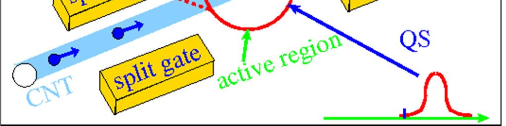
15 A poor man thermometer for CNT Mapping the level shift E and broadening Γto the temperature Tof active region 2 =12 mv hot cold cold hot 1 =8 mv 1 =8 mv justoutside the active region 2 =12 mv inside the active region Τ hot Τ cold ~140 K MURI 12/19/2013
16 Molecular thermometer Scott Meyle, 2014

17 Thermal quantum Hall


18 THz wave sensing experiment Georgetown University (M. Rinzan, P. Barbara group, ) THz sensing with the single-electron tunneling in carbon tube junctions, Nano Letters, 2012 a.c. transport graphene, Jan 30, 2014


19 Theory (Shafraniuk, Nano Letters 2012) setup theory THz photonassisted tunneling through the double barrier quantum dot theory Splitting the single electron tunneling peak of the drain current through the CNT quantum dot at different frequencies the external THz field hf = 7.31, 6.33, 4.67, 3.31, and 3.02 mev a.c. transport graphene, Jan 30, 2014
20 Conclusions Physics of photon-assisted chiral tunneling in graphene and carbon nanotube quantum dots along with the intrinsic coherence, high mobility, and low dimensionality is very important. Using the Klein tunneling in graphene and in CNT opens new exciting opportunities to improving of the a.c. electron transport. Recent publications S. E. Shafraniuk, Electromagnetic properties of graphene junctions, European Physical Journal, B 80, (2011). S. Shafranjuk, Graphene and Carbon Nanotube Quantum Dot Sensors of the THz Waves, In: 'Nanotechnology', Studium Press LLC, USA, Vol. 10: Nanosensing (2012). S. E. M. Rinzan, G. Jenkins, H. D. Drew, S. Shafranjuk, and P. Barbara, Carbon Nanotube Quantum Dots As Highly Sensitive Terahertz-Cooled Spectrometers, Nano Lett.,2012, 12(6),pp ; DOI: /nl300975h Future plans Interpretation of experimental data. Scaling up to large arrays of nanosensors. 20
21 Let Us Meet Again We welcome you all to our future conferences of OMICS Group International Please Visit: Contact us at
About OMICS Group Conferences
 About OMICS Group OMICS Group International is an amalgamation of Open Access publications and worldwide international science conferences and events. Established in the year 2007 with the sole aim of
annually with the support of more than 1000 scientific associations and 30,00
 bout OMICS Group OMICS Group International is an amalgamation of Open Access publications and worldwide international science conferences and events. Established in the yea 2007 with the sole aim of making
OMICS Group International is an amalgamation of Open Access publications
 About OMICS Group OMICS Group International is an amalgamation of Open Access publications and worldwide international science conferences and events. Established in the year 007 with the sole aim of making
About OMICS Group Conferences
 About OMICS Group OMICS Group International is an amalgamation of Open Access publications and worldwide international science conferences and events. Established in the year 2007 with the sole aim of
OMICS Group International is an amalgamation of Open Access publications and worldwide international science conferences and events.
 OMICS Group International is an amalgamation of Open Access publications and worldwide international science conferences and events. Established in the year 2007 with the sole aim of making the information
OMICS Group International is an amalgamation of Open Access publications
 About OMICS Group OMICS Group International is an amalgamation of Open Access publications and worldwide international science conferences and events. Established in the year 2007 with the sole aim of
About OMICS Group Conferences
 About OMICS Group OMICS Group International is an amalgamation of Open Access publications and worldwide international science conferences and events. Established in the year 2007 with the sole aim of
About OMICS Group Conferences
 About MICS Group MICS Group International is an amalgamation of pen Access publications and worldwide international science conferences and events. Established in the year 2007 with the sole aim of making
OMICS Group International is an amalgamation of Open Access publications
 About OMICS Group OMICS Group International is an amalgamation of Open Access publications and worldwide international science conferences and events. Established in the year 2007 with the sole aim of
Design and development of novel reagents for rapid and Selective extraction and separation of selected
 About OMICS Group OMICS Group International is an amalgamation of Open Access publications and worldwide international science conferences and events. Established in the year 2007 with the sole aim of
About OMICS Group Conferences
 About OMICS Group OMICS Group International is an amalgamation of Open Access publications and worldwide international science conferences and events. Established in the year 2007 with the sole aim of
About OMICS Group Conferences
 About OMICS Group OMICS Group International is an amalgamation of Open Access publications and worldwide international science conferences and events. Established in the year 27 with the sole aim of making
OMICS International Conferences
 About OMICS Group OMICS Group is an amalgamation of Open Access Publications and worldwide international science conferences and events. Established in the year 2007 with the sole aim of making the information
About OMICS Group Conferences
 About OMICS Group OMICS Group International is an amalgamation of Open Access publications and worldwide international science conferences and events. Established in the year 2007 with the sole aim of
Terahertz sensing and imaging based on carbon nanotubes:
 Terahertz sensing and imaging based on carbon nanotubes: Frequency-selective detection and near-field imaging Yukio Kawano RIKEN, JST PRESTO ykawano@riken.jp http://www.riken.jp/lab-www/adv_device/kawano/index.html
GRAPHENE the first 2D crystal lattice
 GRAPHENE the first 2D crystal lattice dimensionality of carbon diamond, graphite GRAPHENE realized in 2004 (Novoselov, Science 306, 2004) carbon nanotubes fullerenes, buckyballs what s so special about
Quantum Confinement in Graphene
 Quantum Confinement in Graphene from quasi-localization to chaotic billards MMM dominikus kölbl 13.10.08 1 / 27 Outline some facts about graphene quasibound states in graphene numerical calculation of
Solid State Device Fundamentals
 Solid State Device Fundamentals ENS 345 Lecture Course by Alexander M. Zaitsev alexander.zaitsev@csi.cuny.edu Tel: 718 982 2812 Office 4N101b 1 Outline - Goals of the course. What is electronic device?
Solid State Device Fundamentals
 Solid State Device Fundamentals ENS 345 Lecture Course by Alexander M. Zaitsev alexander.zaitsev@csi.cuny.edu Tel: 718 982 2812 Office 4N101b 1 Outline - Goals of the course. What is electronic device?
SUPPLEMENTARY INFORMATION
 DOI: 1.138/NNANO.215.33 Epitaxial graphene quantum dots for high-performance terahertz bolometers Abdel El Fatimy *, Rachael L. Myers-Ward, Anthony K. Boyd, Kevin M. Daniels, D. Kurt Gaskill, and Paola
OMICS Group International is an amalgamation of Open Access publications
 About OMICS Group OMICS Group International is an amalgamation of Open Access publications and worldwide international science conferences and events. Established in the year 2007 with the sole aim of
OMICS Group International is an amalgamation of Open Access publications
 About OMICS Group OMICS Group International is an amalgamation of Open Access publications and worldwide international science conferences and events. Established in the year 2007 with the sole aim of
Classification of Solids
 Classification of Solids Classification by conductivity, which is related to the band structure: (Filled bands are shown dark; D(E) = Density of states) Class Electron Density Density of States D(E) Examples
Transport through Andreev Bound States in a Superconductor-Quantum Dot-Graphene System
 Transport through Andreev Bound States in a Superconductor-Quantum Dot-Graphene System Nadya Mason Travis Dirk, Yung-Fu Chen, Cesar Chialvo Taylor Hughes, Siddhartha Lal, Bruno Uchoa Paul Goldbart University
About OMICS Group Conferences
 About OMICS Group OMICS Group International is an amalgamation of Open Access publications and worldwide international science conferences and events. Established in the year 2007 with the sole aim of
Graphite, graphene and relativistic electrons
 Graphite, graphene and relativistic electrons Introduction Physics of E. graphene Y. Andrei Experiments Rutgers University Transport electric field effect Quantum Hall Effect chiral fermions STM Dirac
MSE 310/ECE 340: Electrical Properties of Materials Fall 2014 Department of Materials Science and Engineering Boise State University
 MSE 310/ECE 340: Electrical Properties of Materials Fall 2014 Department of Materials Science and Engineering Boise State University Practice Final Exam 1 Read the questions carefully Label all figures
About OMICS Group. place through debates, round table discussions, poster presentations, workshops, symposia and exhibitions.
 About OMICS Group OMICS Group International is an amalgamation of Open Access publications and worldwide international science conferences and events. Established in the year 2007 with the sole aim of
Graphene and Carbon Nanotubes
 Graphene and Carbon Nanotubes 1 atom thick films of graphite atomic chicken wire Novoselov et al - Science 306, 666 (004) 100μm Geim s group at Manchester Novoselov et al - Nature 438, 197 (005) Kim-Stormer
Carbon based Nanoscale Electronics
 Carbon based Nanoscale Electronics 09 02 200802 2008 ME class Outline driving force for the carbon nanomaterial electronic properties of fullerene exploration of electronic carbon nanotube gold rush of
From nanophysics research labs to cell phones. Dr. András Halbritter Department of Physics associate professor
 From nanophysics research labs to cell phones Dr. András Halbritter Department of Physics associate professor Curriculum Vitae Birth: 1976. High-school graduation: 1994. Master degree: 1999. PhD: 2003.
(a) (b) Supplementary Figure 1. (a) (b) (a) Supplementary Figure 2. (a) (b) (c) (d) (e)
 (b) Supplementary Figure 1. (a) (b) (a) Supplementary Figure 2. (a) (b) (c) (d) (e)") (a) (b) Supplementary Figure 1. (a) An AFM image of the device after the formation of the contact electrodes and the top gate dielectric Al 2 O 3. (b) A line scan performed along the white dashed line
(a) (b) Supplementary Figure 1. (a) An AFM image of the device after the formation of the contact electrodes and the top gate dielectric Al 2 O 3. (b) A line scan performed along the white dashed line
Nanomaterials and their Optical Applications
 Nanomaterials and their Optical Applications Winter Semester 2013 Lecture 02 rachel.grange@uni-jena.de http://www.iap.uni-jena.de/multiphoton Lecture 2: outline 2 Introduction to Nanophotonics Theoretical
Seminars in Nanosystems - I
 Seminars in Nanosystems - I Winter Semester 2011/2012 Dr. Emanuela Margapoti Emanuela.Margapoti@wsi.tum.de Dr. Gregor Koblmüller Gregor.Koblmueller@wsi.tum.de Seminar Room at ZNN 1 floor Topics of the
LECTURE 3: Refrigeration
 LECTURE 3: Refrigeration Refrigeration on-chip Thermoelectric refrigeration Peltier refrigerators, Peltier 1834 Thermionic refrigeration, Mahan, 1994 Korotkov and Likharev, 1999 Quantum-dot refrigerator,
Final exam. Introduction to Nanotechnology. Name: Student number:
 1 Final exam. Introduction to Nanotechnology Name: Student number: 1. (a) What is the definition for a cluster size-wise? (3%) (b) Calculate the energy separation near the Fermi surface of a metallic cluster
Wafer-scale fabrication of graphene
 Wafer-scale fabrication of graphene Sten Vollebregt, MSc Delft University of Technology, Delft Institute of Mircosystems and Nanotechnology Delft University of Technology Challenge the future Delft University
Use of Multi-Walled Carbon Nanotubes for UV radiation detection
 Use of Multi-Walled Carbon Nanotubes for UV radiation detection Viviana Carillo 11th Topical Seminar on Innovative Particle and Radiation Detectors (IPRD08) 1-4 October 2008 Siena, Italy A new nanostructured
The Physics of Nanoelectronics
 The Physics of Nanoelectronics Transport and Fluctuation Phenomena at Low Temperatures Tero T. Heikkilä Low Temperature Laboratory, Aalto University, Finland OXFORD UNIVERSITY PRESS Contents List of symbols
Supporting Information
 Electronic Supplementary Material (ESI) for Nanoscale. This journal is The Royal Society of Chemistry 2015 Supporting Information Single Layer Lead Iodide: Computational Exploration of Structural, Electronic
CARLETON UNIVERSITY. FINAL EXAMINATION December 2016
 CARLETON UNIVERSITY FINAL EXAMINATION December 2016 DURATION: 3 HOURS Department Name & Course Number: Electronics 4705 Course Instructor(s): Tom Smy AUTHORIZED MEMORANDA CALCULATOR (Not Programmable)
Graphene photodetectors with ultra-broadband and high responsivity at room temperature
 SUPPLEMENTARY INFORMATION DOI: 10.1038/NNANO.2014.31 Graphene photodetectors with ultra-broadband and high responsivity at room temperature Chang-Hua Liu 1, You-Chia Chang 2, Ted Norris 1.2* and Zhaohui
UvA-DARE (Digital Academic Repository) Charge carrier dynamics in photovoltaic materials Jensen, S.A. Link to publication
 Charge carrier dynamics in photovoltaic materials Jensen, S.A. Link to publication") UvA-DARE (Digital Academic Repository) Charge carrier dynamics in photovoltaic materials Jensen, S.A. Link to publication Citation for published version (APA): Jensen, S. A. (2014). Charge carrier dynamics
UvA-DARE (Digital Academic Repository) Charge carrier dynamics in photovoltaic materials Jensen, S.A. Link to publication Citation for published version (APA): Jensen, S. A. (2014). Charge carrier dynamics
ᣂቇⴚ㗔 䇸䉮䊮䊏䊠䊷䊁䉞䉪䉴䈮䉋䉎 䊂䉱䉟䊮䋺ⶄว 㑐䈫㕖ᐔⴧ䉻䉟䊅䊚䉪䉴䇹 ᐔᚑ22ᐕᐲ ળ䇮2011ᐕ3 4ᣣ䇮 ੩ᄢቇᧄㇹ䉨䊞䊮䊌䉴 㗄 A02 ኒᐲ 㑐ᢙᴺℂ 䈮ၮ䈨䈒㕖ᐔⴧ 䊅䊉䉴䉬䊷䊦㔚 વዉ䉻䉟䊅䊚䉪䉴 ઍ ᄢᎿ ㆺ
 22201134 A02 GCOE Si device (further downsizing) Novel nanostructures (such as atomic chain) Nanoscale multi-terminal resistance measurement Carbon nanotube transistor Atomic switch Interplay:l Dynamics:
ME 4875/MTE C16. Introduction to Nanomaterials and Nanotechnology. Lecture 2 - Applications of Nanomaterials + Projects
 ME 4875/MTE 575 - C16 Introduction to Nanomaterials and Nanotechnology Lecture 2 - Applications of Nanomaterials + Projects 1 Project Teams of 4 students each Literature review of one application of nanotechnology
Semiconductor Physical Electronics
 Semiconductor Physical Electronics Sheng S. Li Semiconductor Physical Electronics Second Edition With 230 Figures Sheng S. Li Department of Electrical and Computer Engineering University of Florida Gainesville,
How a single defect can affect silicon nano-devices. Ted Thorbeck
 How a single defect can affect silicon nano-devices Ted Thorbeck tedt@nist.gov The Big Idea As MOS-FETs continue to shrink, single atomic scale defects are beginning to affect device performance Gate Source
From optical graphene to topological insulator
 From optical graphene to topological insulator Xiangdong Zhang Beijing Institute of Technology (BIT), China zhangxd@bit.edu.cn Collaborator: Wei Zhong (PhD student, BNU) Outline Background: From solid
Lecture 20: Semiconductor Structures Kittel Ch 17, p , extra material in the class notes
 Lecture 20: Semiconductor Structures Kittel Ch 17, p 494-503, 507-511 + extra material in the class notes MOS Structure Layer Structure metal Oxide insulator Semiconductor Semiconductor Large-gap Semiconductor
Designing a Carbon Nanotube Field-Effect Transistor with High Transition Frequency for Ultra-Wideband Application
 Engineering, 2017, 9, 22-35 http://www.scirp.org/journal/eng ISSN Online: 1947-394X ISSN Print: 1947-3931 Designing a Carbon Nanotube Field-Effect Transistor with High Transition Frequency for Ultra-Wideband
Carbon Nanomaterials
 Carbon Nanomaterials STM Image 7 nm AFM Image Fullerenes C 60 was established by mass spectrographic analysis by Kroto and Smalley in 1985 C 60 is called a buckminsterfullerene or buckyball due to resemblance
4. TITLE AND SUBTITLE 5a. CONTRACT NUMBER. 6. AUTHOR(S) 5d. PROJECT NUMBER
 5d. PROJECT NUMBER") REPORT DOCUMENTATION PAGE Form Approved OMB No. 0704-0188 Public reporting burden for this collection of information is estimated to average 1 hour per response, including the time for reviewing instructions,
REPORT DOCUMENTATION PAGE Form Approved OMB No. 0704-0188 Public reporting burden for this collection of information is estimated to average 1 hour per response, including the time for reviewing instructions,
Monolayer Semiconductors
 Monolayer Semiconductors Gilbert Arias California State University San Bernardino University of Washington INT REU, 2013 Advisor: Xiaodong Xu (Dated: August 24, 2013) Abstract Silicon may be unable to
Black phosphorus: A new bandgap tuning knob
 Black phosphorus: A new bandgap tuning knob Rafael Roldán and Andres Castellanos-Gomez Modern electronics rely on devices whose functionality can be adjusted by the end-user with an external knob. A new
I-V characteristics model for Carbon Nanotube Field Effect Transistors
 International Journal of Engineering & Technology IJET-IJENS Vol:14 No:04 33 I-V characteristics model for Carbon Nanotube Field Effect Transistors Rebiha Marki, Chérifa Azizi and Mourad Zaabat. Abstract--
Nanoscale optical circuits: controlling light using localized surface plasmon resonances
 Nanoscale optical circuits: controlling light using localized surface plasmon resonances T. J. Davis, D. E. Gómez and K. C. Vernon CSIRO Materials Science and Engineering Localized surface plasmon (LSP)
About OMICS International Conferences
 About OMICS Group OMICS Group International is an amalgamation of Open Access publications and worldwide international science conferences and events. Established in the year 2007 with the sole aim of
Terahertz Lasers Based on Intersubband Transitions
 Terahertz Lasers Based on Intersubband Transitions Personnel B. Williams, H. Callebaut, S. Kumar, and Q. Hu, in collaboration with J. Reno Sponsorship NSF, ARO, AFOSR,and NASA Semiconductor quantum wells
Nanoscale Heat Transfer and Information Technology
 Response to K.E. Goodson Nanoscale Heat Transfer and Information Technology Gang Chen Mechanical Engineering Department Massachusetts Institute of Technology Cambridge, MA 02139 Rohsenow Symposium on Future
TRANSVERSE SPIN TRANSPORT IN GRAPHENE
 International Journal of Modern Physics B Vol. 23, Nos. 12 & 13 (2009) 2641 2646 World Scientific Publishing Company TRANSVERSE SPIN TRANSPORT IN GRAPHENE TARIQ M. G. MOHIUDDIN, A. A. ZHUKOV, D. C. ELIAS,
Temperature dependence of Andreev spectra in a superconducting carbon nanotube quantum dot
 Temperature dependence of Andreev spectra in a superconducting carbon nanotube quantum dot A. Kumar, M. Gaim, D. Steininger, A. Levy Yeyati, A. Martín-Rodero, A. K. Hüttel, and C. Strunk Phys. Rev. B 89,
Nonlinear optical conductance in a graphene pn junction in the terahertz regime
 University of Wollongong Research Online Faculty of Engineering - Papers (Archive) Faculty of Engineering and Information Sciences 2010 Nonlinear optical conductance in a graphene pn junction in the terahertz
Semiconductor Theory and Devices
 Semiconductor Theory and Devices Band Theory of Solids Semiconductor Theory Semiconductor Devices Nanotechnology It is evident that many years of research by a great many people, both before and after
Physics of Semiconductors
 Physics of Semiconductors 9 th 2016.6.13 Shingo Katsumoto Department of Physics and Institute for Solid State Physics University of Tokyo Site for uploading answer sheet Outline today Answer to the question
2D MBE Activities in Sheffield. I. Farrer, J. Heffernan Electronic and Electrical Engineering The University of Sheffield
 2D MBE Activities in Sheffield I. Farrer, J. Heffernan Electronic and Electrical Engineering The University of Sheffield Outline Motivation Van der Waals crystals The Transition Metal Di-Chalcogenides
chiral m = n Armchair m = 0 or n = 0 Zigzag m n Chiral Three major categories of nanotube structures can be identified based on the values of m and n
 zigzag armchair Three major categories of nanotube structures can be identified based on the values of m and n m = n Armchair m = 0 or n = 0 Zigzag m n Chiral Nature 391, 59, (1998) chiral J. Tersoff,
Graphene Canada Montreal Oct. 16, 2015 (International Year of Light)
") Luminescence Properties of Graphene A. Beltaos 1,2,3, A. Bergren 1, K. Bosnick 1, N. Pekas 1, A. Matković 4, A. Meldrum 2 1 National Institute for Nanotechnology (NINT), 11421 Saskatchewan Drive, Edmonton,
Luminescence Properties of Graphene A. Beltaos 1,2,3, A. Bergren 1, K. Bosnick 1, N. Pekas 1, A. Matković 4, A. Meldrum 2 1 National Institute for Nanotechnology (NINT), 11421 Saskatchewan Drive, Edmonton,
Supplementary Figure 1. Supplementary Figure 1 Characterization of another locally gated PN junction based on boron
 Supplementary Figure 1 Supplementary Figure 1 Characterization of another locally gated PN junction based on boron nitride and few-layer black phosphorus (device S1). (a) Optical micrograph of device S1.
Diameter Optimization for Highest Degree of Ballisticity of Carbon Nanotube Field Effect Transistors I. Khan, O. Morshed and S. M.
 Diameter Optimization for Highest Degree of Ballisticity of Carbon Nanotube Field Effect Transistors I. Khan, O. Morshed and S. M. Mominuzzaman Department of Electrical and Electronic Engineering, Bangladesh
Nanostructures. Lecture 13 OUTLINE
 Nanostructures MTX9100 Nanomaterials Lecture 13 OUTLINE -What is quantum confinement? - How can zero-dimensional materials be used? -What are one dimensional structures? -Why does graphene attract so much
Supplementary Figure 1. Selected area electron diffraction (SAED) of bilayer graphene and tblg. (a) AB
 of bilayer graphene and tblg. (a) AB") Supplementary Figure 1. Selected area electron diffraction (SAED) of bilayer graphene and tblg. (a) AB stacked bilayer graphene (b), (c), (d), (e), and (f) are twisted bilayer graphene with twist angle
Supplementary Figure 1. Selected area electron diffraction (SAED) of bilayer graphene and tblg. (a) AB stacked bilayer graphene (b), (c), (d), (e), and (f) are twisted bilayer graphene with twist angle
Scientific Program. Opening and Welcome Victor Lopez Richard Quantum dot architecture for 15:30-16:00
 Scientific Program Monday, September 18 12:00-13:00 Registration 13:00-15:00 Lunch 15:00-15:30 Opening and Welcome Victor Lopez Richard Quantum dot architecture for 15:30-16:00 memristive and memcapacitive
Sheng S. Li. Semiconductor Physical Electronics. Second Edition. With 230 Figures. 4) Springer
 Springer") Sheng S. Li Semiconductor Physical Electronics Second Edition With 230 Figures 4) Springer Contents Preface 1. Classification of Solids and Crystal Structure 1 1.1 Introduction 1 1.2 The Bravais Lattice
Sheng S. Li Semiconductor Physical Electronics Second Edition With 230 Figures 4) Springer Contents Preface 1. Classification of Solids and Crystal Structure 1 1.1 Introduction 1 1.2 The Bravais Lattice
CHAPTER EIGHT: PHOTONIC CRYSTALS: MATERIALS, END USES, AND MARKETS, MATERIALS PROPERTIES... 78
 CHAPTER ONE: INTRODUCTION... 1 STUDY BACKGROUND... 1 STUDY GOALS AND OBJECTIVES... 1 INTENDED AUDIENCE... 2 SCOPE AND FORMAT... 2 INFORMATION SOURCES AND METHODOLOGY... 3 ANALYST CREDENTIALS... 4 RELATED
Graphene. Tianyu Ye November 30th, 2011
 Graphene Tianyu Ye November 30th, 2011 Outline What is graphene? How to make graphene? (Exfoliation, Epitaxial, CVD) Is it graphene? (Identification methods) Transport properties; Other properties; Applications;
UNIT I: Electronic Materials.
 SIDDHARTH INSTITUTE OF ENGINEERING & TECHNOLOGY :: PUTTUR Siddharth Nagar, Narayanavanam Road 517583 QUESTION BANK (DESCRIPTIVE) Subject with Code: SEMICONDUCTOR PHYSICS (18HS0851) Course & Branch: B.Tech
Physics and Material Science of Semiconductor Nanostructures
 Physics and Material Science of Semiconductor Nanostructures PHYS 570P Prof. Oana Malis Email: omalis@purdue.edu Course website: http://www.physics.purdue.edu/academic_programs/courses/phys570p/ 1 Course
Device 3D. 3D Device Simulator. Nano Scale Devices. Fin FET
 Device 3D 3D Device Simulator Device 3D is a physics based 3D device simulator for any device type and includes material properties for the commonly used semiconductor materials in use today. The physical
Cover Page. The handle holds various files of this Leiden University dissertation
 Cover Page The handle http://hdl.handle.net/1887/24306 holds various files of this Leiden University dissertation Author: Verhagen, T.G.A. Title: Magnetism and magnetization dynamics in thin film ferromagnets
Magneto-plasmonic effects in epitaxial graphene
 Magneto-plasmonic effects in epitaxial graphene Alexey Kuzmenko University of Geneva Graphene Nanophotonics Benasque, 4 March 13 Collaborators I. Crassee, N. Ubrig, I. Nedoliuk, J. Levallois, D. van der
3-month progress Report
 3-month progress Report Graphene Devices and Circuits Supervisor Dr. P.A Childs Table of Content Abstract... 1 1. Introduction... 1 1.1 Graphene gold rush... 1 1.2 Properties of graphene... 3 1.3 Semiconductor
NiCl2 Solution concentration. Etching Duration. Aspect ratio. Experiment Atmosphere Temperature. Length(µm) Width (nm) Ar:H2=9:1, 150Pa
 Width (nm) Ar:H2=9:1, 150Pa") Experiment Atmosphere Temperature #1 # 2 # 3 # 4 # 5 # 6 # 7 # 8 # 9 # 10 Ar:H2=9:1, 150Pa Ar:H2=9:1, 150Pa Ar:H2=9:1, 150Pa Ar:H2=9:1, 150Pa Ar:H2=9:1, 150Pa Ar:H2=9:1, 150Pa Ar:H2=9:1, 150Pa Ar:H2=9:1,
Experiment Atmosphere Temperature #1 # 2 # 3 # 4 # 5 # 6 # 7 # 8 # 9 # 10 Ar:H2=9:1, 150Pa Ar:H2=9:1, 150Pa Ar:H2=9:1, 150Pa Ar:H2=9:1, 150Pa Ar:H2=9:1, 150Pa Ar:H2=9:1, 150Pa Ar:H2=9:1, 150Pa Ar:H2=9:1,
SUPPLEMENTARY INFORMATION
 SUPPLEMENTARY INFORMATION DOI: 10.1038/NNANO.2011.138 Graphene Nanoribbons with Smooth Edges as Quantum Wires Xinran Wang, Yijian Ouyang, Liying Jiao, Hailiang Wang, Liming Xie, Justin Wu, Jing Guo, and
Fermi Level Pinning at Electrical Metal Contacts. of Monolayer Molybdenum Dichalcogenides
 Supporting information Fermi Level Pinning at Electrical Metal Contacts of Monolayer Molybdenum Dichalcogenides Changsik Kim 1,, Inyong Moon 1,, Daeyeong Lee 1, Min Sup Choi 1, Faisal Ahmed 1,2, Seunggeol
Lecture 20 - Semiconductor Structures
 Lecture 0: Structures Kittel Ch 17, p 494-503, 507-511 + extra material in the class notes MOS Structure metal Layer Structure Physics 460 F 006 Lect 0 1 Outline What is a semiconductor Structure? Created
Nanoscience, MCC026 2nd quarter, fall Quantum Transport, Lecture 1/2. Tomas Löfwander Applied Quantum Physics Lab
 Nanoscience, MCC026 2nd quarter, fall 2012 Quantum Transport, Lecture 1/2 Tomas Löfwander Applied Quantum Physics Lab Quantum Transport Nanoscience: Quantum transport: control and making of useful things
Nonlinear Electrodynamics and Optics of Graphene
 Nonlinear Electrodynamics and Optics of Graphene S. A. Mikhailov and N. A. Savostianova University of Augsburg, Institute of Physics, Universitätsstr. 1, 86159 Augsburg, Germany E-mail: sergey.mikhailov@physik.uni-augsburg.de
Introduction to Nanotechnology Chapter 5 Carbon Nanostructures Lecture 1
 Introduction to Nanotechnology Chapter 5 Carbon Nanostructures Lecture 1 ChiiDong Chen Institute of Physics, Academia Sinica chiidong@phys.sinica.edu.tw 02 27896766 Section 5.2.1 Nature of the Carbon Bond
CHAPTER 11 Semiconductor Theory and Devices
 CHAPTER 11 Semiconductor Theory and Devices 11.1 Band Theory of Solids 11.2 Semiconductor Theory 11.3 Semiconductor Devices 11.4 Nanotechnology It is evident that many years of research by a great many
Electron Interactions and Nanotube Fluorescence Spectroscopy C.L. Kane & E.J. Mele
 Electron Interactions and Nanotube Fluorescence Spectroscopy C.L. Kane & E.J. Mele Large radius theory of optical transitions in semiconducting nanotubes derived from low energy theory of graphene Phys.
Design Optimization for 4.1-THZ Quantum Cascade Lasers
 Design Optimization for 4.1-THZ Quantum Cascade Lasers F. Esmailifard*, M. K. Moravvej-Farshi* and K. Saghafi** Abstract: We present an optimized design for GaAs/AlGaAs quantum cascade lasers operating
Graphene Novel Material for Nanoelectronics
 Graphene Novel Material for Nanoelectronics Shintaro Sato Naoki Harada Daiyu Kondo Mari Ohfuchi (Manuscript received May 12, 2009) Graphene is a flat monolayer of carbon atoms with a two-dimensional honeycomb
Supplementary Figure S1. AFM images of GraNRs grown with standard growth process. Each of these pictures show GraNRs prepared independently,
 Supplementary Figure S1. AFM images of GraNRs grown with standard growth process. Each of these pictures show GraNRs prepared independently, suggesting that the results is reproducible. Supplementary Figure
Modern Physics for Scientists and Engineers International Edition, 4th Edition
 Modern Physics for Scientists and Engineers International Edition, 4th Edition http://optics.hanyang.ac.kr/~shsong 1. THE BIRTH OF MODERN PHYSICS 2. SPECIAL THEORY OF RELATIVITY 3. THE EXPERIMENTAL BASIS
Semiconductor Nanowires: Motivation
 Semiconductor Nanowires: Motivation Patterning into sub 50 nm range is difficult with optical lithography. Self-organized growth of nanowires enables 2D confinement of carriers with large splitting of
Ferromagnetism and Anomalous Hall Effect in Graphene
 Ferromagnetism and Anomalous Hall Effect in Graphene Jing Shi Department of Physics & Astronomy, University of California, Riverside Graphene/YIG Introduction Outline Proximity induced ferromagnetism Quantized
arxiv:cond-mat/ v1 [cond-mat.mes-hall] 27 Nov 2001
![arxiv:cond-mat/ v1 [cond-mat.mes-hall] 27 Nov 2001](/thumbs/72/66784898.jpg "arxiv:cond-mat/ v1 [cond-mat.mes-hall] 27 Nov 2001") Published in: Single-Electron Tunneling and Mesoscopic Devices, edited by H. Koch and H. Lübbig (Springer, Berlin, 1992): pp. 175 179. arxiv:cond-mat/0111505v1 [cond-mat.mes-hall] 27 Nov 2001 Resonant
Published in: Single-Electron Tunneling and Mesoscopic Devices, edited by H. Koch and H. Lübbig (Springer, Berlin, 1992): pp. 175 179. arxiv:cond-mat/0111505v1 [cond-mat.mes-hall] 27 Nov 2001 Resonant
Supplementary Information
 Supplementary Information Ambient effects on electrical characteristics of CVD-grown monolayer MoS 2 field-effect transistors Jae-Hyuk Ahn, 1,2 William M. Parkin, 1 Carl H. Naylor, 1 A. T. Charlie Johnson,
Electro-Thermal Transport in Silicon and Carbon Nanotube Devices E. Pop, D. Mann, J. Rowlette, K. Goodson and H. Dai
 Electro-Thermal Transport in Silicon and Carbon Nanotube Devices E. Pop, D. Mann, J. Rowlette, K. Goodson and H. Dai E. Pop, 1,2 D. Mann, 1 J. Rowlette, 2 K. Goodson 2 and H. Dai 1 Dept. of 1 Chemistry
Graphene transistor. Seminar I a. Mentor: doc. dr. Tomaž Rejec. April Abstract
 Graphene transistor Seminar I a Jan Srpčič Mentor: doc. dr. Tomaž Rejec April 2015 Abstract The topic of this seminar is graphene and its possible applications in the field of electronics, most notably