Physics of Semiconductors
|
|
|
- Gillian Lucas
- 5 years ago
- Views:
Transcription

1 Physics of Semiconductors 9 th Shingo Katsumoto Department of Physics and Institute for Solid State Physics University of Tokyo

2 Site for uploading answer sheet
3 Outline today Answer to the question paused in the last week Heterojunction and quantum confinement to 2-dimensional systems Heterojunction connection rule Quantum well Quantum barrier Double barrier Resonant diode Superlattice Modulation doping
4 My question in the last week J Consider an ideal light emitting diode, which has no non-radiative recombination. Every injected carrier emits a photon with the energy E g. Now apply a voltage V 1 < E g /e and a current J 1 flows. The power of light emission is P L = E g J 1 /e. On the other hand, the electric power source gives the power P S = J 1 V 1, which is smaller than P L! Does the LED create energy? Or what is happening inside the LED? J V 1 E g e V


5 An experiment 2.4 V: µm Green! Blue: 0.45 µm -> 2.76eV
6 pn junction as a heat pump E E D(E) f c (E) Only carriers with high kinetic energies can diffuse into the other layer Environment heat bath Evaporation cooling occurs Electric power source pn junction Photon

7 Evaporation cooling of atoms Magnetic trap Atoms in MOT Zeemann splitting 4 cm f rf Courtesy: Prof. Torii hν E
8 Ch.3 Heterojunctions and quantum confinement to two-dimensional systems

9 Nobel prize for semiconductor heterostructure
10 Heterojunction and envelope function Bloch type wavefuntion: Lattice periodic function band structure Plane wave Envelope function Lattice Hamiltonian: Perturbation potential: Bloch functions Envelope function


11 Heterojunction and envelope function Inverse Fourier transformation Schrödinger equation with effective mass: Effective mass approximation Heterojunction: difference in and normalize into step potential at the interface:

.")
12 Anderson s rule R. L. Anderson, IBM J. Res. Dev. 4, 283 (1960).
 Graphene Lattice constant")
13 II-VI, III-V, VI combinations GaN ZnO Energy gap (ev) Graphene Lattice constant (Å)

")

14 Molecular beam epitaxy (MBE) RHEED Substrate Ga Al In As Si


15 van del Waals heterostructure A. K. Geim and I. V. Grigorieva Nature 499, 419 (2013).
16 Quantum well V 0 V(x) States localized inside the well: E < V 0 L/2 L/2 x
17 Quantum well Continuous: Differentiable:


18 Quantum well
19 Optical absorption in quantum well lh Envelope function Lattice periodic function E g Two dimensional density of states: hh

20 Optical absorption in quantum well
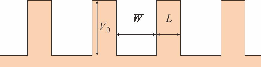
21 Quantum barrier A 1 (k) B 1 (k) 1 Q 2 M T A 2 (k) B 2 (k) Transfer matrix: M T M T for a barrier width L height V 0 Inside the barrier Boundary condition:
22 Transfer matrix for a square barrier t, r : complex transmission and reflection coefficients


23 Double barrier transmission


24 Double barrier transmission Resonant transmission


25 Double barrier conduction Source ev ss Drain Transmission coefficient light hole heavy hole E/V 0


26 Double barrier conduction Source ev ss Drain z I ss k z V ss k y k x
27 Double barrier and wave packet Resonant T =1? 1. Immediately go through 2. Take some time and go through 3. Mostly be reflected by the potential 4. Others

28 Double barrier and wave packet Quasi qu stationary reflected incoming


29 Semiconductor Superlattice d Raphael Tsu Leo Esaki Bloch theorem Eigenvalue e ±iii


30 Kronig-Penny potential : δ -function series potential
31 Bloch oscillation in solids Cosine band: Bloch oscillation

32 Formation of mini-bands
. N. Sekine et al. Phys. Rev. Lett. 94, 057408 (2005).")
33 Experiment on Bloch oscillation Stark ladder state near infrared THz A Y. Shimada et al. Phys. Rev. Lett. 90, (2003). N. Sekine et al. Phys. Rev. Lett. 94, (2005).

34 Experiment on Bloch oscillation

35 Modulation doping and 2-dimensional electrons Hartree potential Electric field of sheet charge
36 Modulation doping and 2-dimensional electrons Step function Solve self-consistently Schrödinger equation
37 Approximations Airy function Triangular potential Fang-Howard (variational approximation)
38 Electron mobility in MODFET
39 Exercise B-6-13 here is a GaAs (dielectric constant 13) p + n diode grown with molecular beam epitaxy. Doping is abrupt and uniform for both p and n layers. We have cut the grown film to a 1 mm 2 area and measured the differential capacitance with applying the (negative) bias voltage V b and obtained the results summarized in the table on the left. Submission deadline: 6/27 Obtain the built-in potential in unit of V. The measured C contains some experimental errors. Assume that the capacitance is dominated by the doping in the n layer and obtain the donor concentration in the n layer in the unit of cm 3.
Physics of Semiconductors (Problems for report)
") Physics of Semiconductors (Problems for report) Shingo Katsumoto Institute for Solid State Physics, University of Tokyo July, 0 Choose two from the following eight problems and solve them. I. Fundamentals
Physics of Semiconductors (Problems for report) Shingo Katsumoto Institute for Solid State Physics, University of Tokyo July, 0 Choose two from the following eight problems and solve them. I. Fundamentals
Physics of Semiconductors
 Physics of Semiconductors 13 th 2016.7.11 Shingo Katsumoto Department of Physics and Institute for Solid State Physics University of Tokyo Outline today Laughlin s justification Spintronics Two current
Physics of Semiconductors 8 th
 Physics of Semiconductors 8 th 2016.6.6 Shingo Katsumoto Department of Physics, Institute for Solid State Physics University of Tokyo Review of pn junction Estimation of builtin potential Depletion layer
ρ ρ LED access resistances d A W d s n s p p p W the output window size p-layer d p series access resistance d n n-layer series access resistance
 LED access resistances W the output window size p-layer series access resistance d p n-layer series access resistance d n The n-layer series access resistance R = ρ s n where the resistivity of the n-layer
Semiconductor Physical Electronics
 Semiconductor Physical Electronics Sheng S. Li Department of Electrical Engineering University of Florida Gainesville, Florida Plenum Press New York and London Contents CHAPTER 1. Classification of Solids
Chapter 5. Semiconductor Laser
 Chapter 5 Semiconductor Laser 5.0 Introduction Laser is an acronym for light amplification by stimulated emission of radiation. Albert Einstein in 1917 showed that the process of stimulated emission must
Magneto-Optical Properties of Quantum Nanostructures
 Magneto-optics of nanostructures Magneto-Optical Properties of Quantum Nanostructures Milan Orlita Institute of Physics, Charles University Institute of Physics, Academy of Sciences of the Czech Republic
Lecture 20: Semiconductor Structures Kittel Ch 17, p , extra material in the class notes
 Lecture 20: Semiconductor Structures Kittel Ch 17, p 494-503, 507-511 + extra material in the class notes MOS Structure Layer Structure metal Oxide insulator Semiconductor Semiconductor Large-gap Semiconductor
Introduction to Optoelectronic Device Simulation by Joachim Piprek
 NUSOD 5 Tutorial MA Introduction to Optoelectronic Device Simulation by Joachim Piprek Outline:. Introduction: VCSEL Example. Electron Energy Bands 3. Drift-Diffusion Model 4. Thermal Model 5. Gain/Absorption
Quantum Phenomena & Nanotechnology (4B5)
") Quantum Phenomena & Nanotechnology (4B5) The 2-dimensional electron gas (2DEG), Resonant Tunneling diodes, Hot electron transistors Lecture 11 In this lecture, we are going to look at 2-dimensional electron
Quantum Phenomena & Nanotechnology (4B5) The 2-dimensional electron gas (2DEG), Resonant Tunneling diodes, Hot electron transistors Lecture 11 In this lecture, we are going to look at 2-dimensional electron
Sheng S. Li. Semiconductor Physical Electronics. Second Edition. With 230 Figures. 4) Springer
 Springer") Sheng S. Li Semiconductor Physical Electronics Second Edition With 230 Figures 4) Springer Contents Preface 1. Classification of Solids and Crystal Structure 1 1.1 Introduction 1 1.2 The Bravais Lattice
Sheng S. Li Semiconductor Physical Electronics Second Edition With 230 Figures 4) Springer Contents Preface 1. Classification of Solids and Crystal Structure 1 1.1 Introduction 1 1.2 The Bravais Lattice
1. Binary III-V compounds 2 p From which atoms are the 16 binary III-V compounds formed?...column III B, Al, Ga and In...column V N, P, As and Sb...
 PROBLEMS part B, Semiconductor Materials. 2006 1. Binary III-V compounds 2 p From which atoms are the 16 binary III-V compounds formed?...column III B, Al, Ga and In...column V N, P, As and Sb... 2. Semiconductors
Electron Energy, E E = 0. Free electron. 3s Band 2p Band Overlapping energy bands. 3p 3s 2p 2s. 2s Band. Electrons. 1s ATOM SOLID.
 Electron Energy, E Free electron Vacuum level 3p 3s 2p 2s 2s Band 3s Band 2p Band Overlapping energy bands Electrons E = 0 1s ATOM 1s SOLID In a metal the various energy bands overlap to give a single
Self-Assembled InAs Quantum Dots
 Self-Assembled InAs Quantum Dots Steve Lyon Department of Electrical Engineering What are semiconductors What are semiconductor quantum dots How do we make (grow) InAs dots What are some of the properties
PHYSICS OF SEMICONDUCTORS AND THEIR HETEROSTRUCTURES
 PHYSICS OF SEMICONDUCTORS AND THEIR HETEROSTRUCTURES Jasprit Singh University of Michigan McGraw-Hill, Inc. New York St. Louis San Francisco Auckland Bogota Caracas Lisbon London Madrid Mexico Milan Montreal
Electronic and Optoelectronic Properties of Semiconductor Structures
 Electronic and Optoelectronic Properties of Semiconductor Structures Jasprit Singh University of Michigan, Ann Arbor CAMBRIDGE UNIVERSITY PRESS CONTENTS PREFACE INTRODUCTION xiii xiv 1.1 SURVEY OF ADVANCES
Quantum and Non-local Transport Models in Crosslight Device Simulators. Copyright 2008 Crosslight Software Inc.
 Quantum and Non-local Transport Models in Crosslight Device Simulators Copyright 2008 Crosslight Software Inc. 1 Introduction Quantization effects Content Self-consistent charge-potential profile. Space
ET3034TUx Utilization of band gap energy
 ET3034TUx - 3.3.1 - Utilization of band gap energy In the last two weeks we have discussed the working principle of a solar cell and the external parameters that define the performance of a solar cell.
Classification of Solids
 Classification of Solids Classification by conductivity, which is related to the band structure: (Filled bands are shown dark; D(E) = Density of states) Class Electron Density Density of States D(E) Examples
Laser Diodes. Revised: 3/14/14 14: , Henry Zmuda Set 6a Laser Diodes 1
 Laser Diodes Revised: 3/14/14 14:03 2014, Henry Zmuda Set 6a Laser Diodes 1 Semiconductor Lasers The simplest laser of all. 2014, Henry Zmuda Set 6a Laser Diodes 2 Semiconductor Lasers 1. Homojunction
3. Two-dimensional systems
 3. Two-dimensional systems Image from IBM-Almaden 1 Introduction Type I: natural layered structures, e.g., graphite (with C nanostructures) Type II: artificial structures, heterojunctions Great technological
Graphene and Carbon Nanotubes
 Graphene and Carbon Nanotubes 1 atom thick films of graphite atomic chicken wire Novoselov et al - Science 306, 666 (004) 100μm Geim s group at Manchester Novoselov et al - Nature 438, 197 (005) Kim-Stormer
Tunneling transport. Courtesy Prof. S. Sawyer, RPI Also Davies Ch. 5
 unneling transport Courtesy Prof. S. Sawyer, RPI Also Davies Ch. 5 Electron transport properties l e : electronic mean free path l φ : phase coherence length λ F : Fermi wavelength ecture Outline Important
Paper Review. Special Topics in Optical Engineering II (15/1) Minkyu Kim. IEEE Journal of Quantum Electronics, Feb 1985
 Minkyu Kim. IEEE Journal of Quantum Electronics, Feb 1985") Paper Review IEEE Journal of Quantum Electronics, Feb 1985 Contents Semiconductor laser review High speed semiconductor laser Parasitic elements limitations Intermodulation products Intensity noise Large
Paper Review IEEE Journal of Quantum Electronics, Feb 1985 Contents Semiconductor laser review High speed semiconductor laser Parasitic elements limitations Intermodulation products Intensity noise Large
Lecture 20 - Semiconductor Structures
 Lecture 0: Structures Kittel Ch 17, p 494-503, 507-511 + extra material in the class notes MOS Structure metal Layer Structure Physics 460 F 006 Lect 0 1 Outline What is a semiconductor Structure? Created
Nanoscience and Molecular Engineering (ChemE 498A) Semiconductor Nano Devices
 Semiconductor Nano Devices") Reading: The first two readings cover the questions to bands and quasi-electrons/holes. See also problem 4. General Questions: 1. What is the main difference between a metal and a semiconductor or insulator,
Reading: The first two readings cover the questions to bands and quasi-electrons/holes. See also problem 4. General Questions: 1. What is the main difference between a metal and a semiconductor or insulator,
Final Examination EE 130 December 16, 1997 Time allotted: 180 minutes
 Final Examination EE 130 December 16, 1997 Time allotted: 180 minutes Problem 1: Semiconductor Fundamentals [30 points] A uniformly doped silicon sample of length 100µm and cross-sectional area 100µm 2
Stimulated Emission Devices: LASERS
 Stimulated Emission Devices: LASERS 1. Stimulated Emission and Photon Amplification E 2 E 2 E 2 hυ hυ hυ In hυ Out hυ E 1 E 1 E 1 (a) Absorption (b) Spontaneous emission (c) Stimulated emission The Principle
Luminescence basics. Slide # 1
 Luminescence basics Types of luminescence Cathodoluminescence: Luminescence due to recombination of EHPs created by energetic electrons. Example: CL mapping system Photoluminescence: Luminescence due to
QUANTUM WELLS, WIRES AND DOTS
 QUANTUM WELLS, WIRES AND DOTS Theoretical and Computational Physics of Semiconductor Nanostructures Second Edition Paul Harrison The University of Leeds, UK /Cf}\WILEY~ ^INTERSCIENCE JOHN WILEY & SONS,
Session 6: Solid State Physics. Diode
 Session 6: Solid State Physics Diode 1 Outline A B C D E F G H I J 2 Definitions / Assumptions Homojunction: the junction is between two regions of the same material Heterojunction: the junction is between
Solar Cell Materials and Device Characterization
 Solar Cell Materials and Device Characterization April 3, 2012 The University of Toledo, Department of Physics and Astronomy SSARE, PVIC Principles and Varieties of Solar Energy (PHYS 4400) and Fundamentals
Introduction to Semiconductor Integrated Optics
 Introduction to Semiconductor Integrated Optics Hans P. Zappe Artech House Boston London Contents acknowledgments reface itroduction Chapter 1 Basic Electromagnetics 1 1.1 General Relationships 1 1.1.1
Metal Vapour Lasers Use vapoured metal as a gain medium Developed by W. Silfvast (1966) Two types: Ionized Metal vapour (He-Cd) Neutral Metal vapour
 Two types: Ionized Metal vapour (He-Cd) Neutral Metal vapour") Metal Vapour Lasers Use vapoured metal as a gain medium Developed by W. Silfvast (1966) Two types: Ionized Metal vapour (He-Cd) Neutral Metal vapour (Cu) All operate by vaporizing metal in container Helium
Metal Vapour Lasers Use vapoured metal as a gain medium Developed by W. Silfvast (1966) Two types: Ionized Metal vapour (He-Cd) Neutral Metal vapour (Cu) All operate by vaporizing metal in container Helium
Signal regeneration - optical amplifiers
 Signal regeneration - optical amplifiers In any atom or solid, the state of the electrons can change by: 1) Stimulated absorption - in the presence of a light wave, a photon is absorbed, the electron is
Schottky diodes. JFETs - MESFETs - MODFETs
 Technische Universität Graz Institute of Solid State Physics Schottky diodes JFETs - MESFETs - MODFETs Quasi Fermi level When the charge carriers are not in equilibrium the Fermi energy can be different
wave mechanics applied to semiconductor heterostructures
 wave mechanics applied to semiconductor heterostructures GERALD BASTARD les editions de physique Avenue du Hoggar, Zone Industrielle de Courtaboeuf, B.P. 112, 91944 Les Ulis Cedex, France Contents PREFACE
Surfaces, Interfaces, and Layered Devices
 Surfaces, Interfaces, and Layered Devices Building blocks for nanodevices! W. Pauli: God made solids, but surfaces were the work of Devil. Surfaces and Interfaces 1 Interface between a crystal and vacuum
Typical example of the FET: MEtal Semiconductor FET (MESFET)
") Typical example of the FET: MEtal Semiconductor FET (MESFET) Conducting channel (RED) is made of highly doped material. The electron concentration in the channel n = the donor impurity concentration N
Typical example of the FET: MEtal Semiconductor FET (MESFET) Conducting channel (RED) is made of highly doped material. The electron concentration in the channel n = the donor impurity concentration N
LEC E T C U T R U E R E 17 -Photodetectors
 LECTURE 17 -Photodetectors Topics to be covered Photodetectors PIN photodiode Avalanche Photodiode Photodetectors Principle of the p-n junction Photodiode A generic photodiode. Photodetectors Principle
(b) Spontaneous emission. Absorption, spontaneous (random photon) emission and stimulated emission.
 Spontaneous emission. Absorption, spontaneous (random photon) emission and stimulated emission.") Lecture 10 Stimulated Emission Devices Lasers Stimulated emission and light amplification Einstein coefficients Optical fiber amplifiers Gas laser and He-Ne Laser The output spectrum of a gas laser Laser
Lecture 10 Stimulated Emission Devices Lasers Stimulated emission and light amplification Einstein coefficients Optical fiber amplifiers Gas laser and He-Ne Laser The output spectrum of a gas laser Laser
Zeeman splitting of single semiconductor impurities in resonant tunneling heterostructures
 Superlattices and Microstructures, Vol. 2, No. 4, 1996 Zeeman splitting of single semiconductor impurities in resonant tunneling heterostructures M. R. Deshpande, J. W. Sleight, M. A. Reed, R. G. Wheeler
Quiz #1 Practice Problem Set
 Name: Student Number: ELEC 3908 Physical Electronics Quiz #1 Practice Problem Set? Minutes January 22, 2016 - No aids except a non-programmable calculator - All questions must be answered - All questions
Introduction to Sources: Radiative Processes and Population Inversion in Atoms, Molecules, and Semiconductors Atoms and Molecules
 OPTI 500 DEF, Spring 2012, Lecture 2 Introduction to Sources: Radiative Processes and Population Inversion in Atoms, Molecules, and Semiconductors Atoms and Molecules Energy Levels Every atom or molecule
EE 3329 Electronic Devices Syllabus ( Extended Play )
") EE 3329 - Electronic Devices Syllabus EE 3329 Electronic Devices Syllabus ( Extended Play ) The University of Texas at El Paso The following concepts can be part of the syllabus for the Electronic Devices
EE 3329 - Electronic Devices Syllabus EE 3329 Electronic Devices Syllabus ( Extended Play ) The University of Texas at El Paso The following concepts can be part of the syllabus for the Electronic Devices
Schottky Rectifiers Zheng Yang (ERF 3017,
 ECE442 Power Semiconductor Devices and Integrated Circuits Schottky Rectifiers Zheng Yang (ERF 3017, email: yangzhen@uic.edu) Power Schottky Rectifier Structure 2 Metal-Semiconductor Contact The work function
CME 300 Properties of Materials. ANSWERS: Homework 9 November 26, As atoms approach each other in the solid state the quantized energy states:
 CME 300 Properties of Materials ANSWERS: Homework 9 November 26, 2011 As atoms approach each other in the solid state the quantized energy states: are split. This splitting is associated with the wave
Spring Semester 2012 Final Exam
 Spring Semester 2012 Final Exam Note: Show your work, underline results, and always show units. Official exam time: 2.0 hours; an extension of at least 1.0 hour will be granted to anyone. Materials parameters
MSE 310/ECE 340: Electrical Properties of Materials Fall 2014 Department of Materials Science and Engineering Boise State University
 MSE 310/ECE 340: Electrical Properties of Materials Fall 2014 Department of Materials Science and Engineering Boise State University Practice Final Exam 1 Read the questions carefully Label all figures
8. Schottky contacts / JFETs
 Technische Universität Graz Institute of Solid State Physics 8. Schottky contacts / JFETs Nov. 21, 2018 Technische Universität Graz Institute of Solid State Physics metal - semiconductor contacts Photoelectric
Optically-Pumped Ge-on-Si Gain Media: Lasing and Broader Impact
 Optically-Pumped Ge-on-Si Gain Media: Lasing and Broader Impact J. Liu 1, R. Camacho 2, X. Sun 2, J. Bessette 2, Y. Cai 2, X. X. Wang 1, L. C. Kimerling 2 and J. Michel 2 1 Thayer School, Dartmouth College;
Schottky Diodes (M-S Contacts)
") Schottky Diodes (M-S Contacts) Three MITs of the Day Band diagrams for ohmic and rectifying Schottky contacts Similarity to and difference from bipolar junctions on electrostatic and IV characteristics.
Schottky Diodes (M-S Contacts) Three MITs of the Day Band diagrams for ohmic and rectifying Schottky contacts Similarity to and difference from bipolar junctions on electrostatic and IV characteristics.
Semiconductor device structures are traditionally divided into homojunction devices
 0. Introduction: Semiconductor device structures are traditionally divided into homojunction devices (devices consisting of only one type of semiconductor material) and heterojunction devices (consisting
Surfaces, Interfaces, and Layered Devices
 Surfaces, Interfaces, and Layered Devices Building blocks for nanodevices! W. Pauli: God made solids, but surfaces were the work of Devil. Surfaces and Interfaces 1 Role of surface effects in mesoscopic
Optical properties of strain-compensated hybrid InGaN/InGaN/ZnO quantum well lightemitting
 Optical properties of strain-compensated hybrid InGaN/InGaN/ZnO quantum well lightemitting diodes S.-H. Park 1, S.-W. Ryu 1, J.-J. Kim 1, W.-P. Hong 1, H.-M Kim 1, J. Park 2, and Y.-T. Lee 3 1 Department
Avalanche breakdown. Impact ionization causes an avalanche of current. Occurs at low doping
 Avalanche breakdown Impact ionization causes an avalanche of current Occurs at low doping Zener tunneling Electrons tunnel from valence band to conduction band Occurs at high doping Tunneling wave decays
UNIVERSITY OF CALIFORNIA College of Engineering Department of Electrical Engineering and Computer Sciences. EECS 130 Professor Ali Javey Fall 2006
 UNIVERSITY OF CALIFORNIA College of Engineering Department of Electrical Engineering and Computer Sciences EECS 130 Professor Ali Javey Fall 2006 Midterm 2 Name: SID: Closed book. Two sheets of notes are
Single Photon detectors
 Single Photon detectors Outline Motivation for single photon detection Semiconductor; general knowledge and important background Photon detectors: internal and external photoeffect Properties of semiconductor
Semiconductor Module
 Semiconductor Module Optics Seminar July 18, 2018 Yosuke Mizuyama, Ph.D. COMSOL, Inc. The COMSOL Product Suite Governing Equations Semiconductor Schrödinger Equation Semiconductor Optoelectronics, FD Semiconductor
3-1-2 GaSb Quantum Cascade Laser
 3-1-2 GaSb Quantum Cascade Laser A terahertz quantum cascade laser (THz-QCL) using a resonant longitudinal optical (LO) phonon depopulation scheme was successfully demonstrated from a GaSb/AlSb material
Chapter 6: Light-Emitting Diodes
 Chapter 6: Light-Emitting Diodes Photoluminescence and electroluminescence Basic transitions Luminescence efficiency Light-emitting diodes Internal quantum efficiency External quantum efficiency Device
Computer Aided Design of GaN Light-Emitting Diodes. Copyright 2006 Crosslight Software Inc.
 Computer Aided Design of GaN Light-Emitting Diodes Copyright 2006 Crosslight Software Inc. www.crosslight.com 1 2 Contents Available tools and modules. Simulation of IQE droop. Design of superlattice.
Lecture 18: Semiconductors - continued (Kittel Ch. 8)
") Lecture 18: Semiconductors - continued (Kittel Ch. 8) + a - Donors and acceptors J U,e e J q,e Transport of charge and energy h E J q,e J U,h Physics 460 F 2006 Lect 18 1 Outline More on concentrations
Lecture 18: Semiconductors - continued (Kittel Ch. 8) + a - Donors and acceptors J U,e e J q,e Transport of charge and energy h E J q,e J U,h Physics 460 F 2006 Lect 18 1 Outline More on concentrations
Optical Properties of Semiconductors. Prof.P. Ravindran, Department of Physics, Central University of Tamil Nadu, India
 Optical Properties of Semiconductors 1 Prof.P. Ravindran, Department of Physics, Central University of Tamil Nadu, India http://folk.uio.no/ravi/semi2013 Light Matter Interaction Response to external electric
FIBER OPTICS. Prof. R.K. Shevgaonkar. Department of Electrical Engineering. Indian Institute of Technology, Bombay. Lecture: 12.
 FIBER OPTICS Prof. R.K. Shevgaonkar Department of Electrical Engineering Indian Institute of Technology, Bombay Lecture: 12 Optical Sources Fiber Optics, Prof. R.K. Shevgaonkar, Dept. of Electrical Engineering,
Laser Basics. What happens when light (or photon) interact with a matter? Assume photon energy is compatible with energy transition levels.
 interact with a matter? Assume photon energy is compatible with energy transition levels.") What happens when light (or photon) interact with a matter? Assume photon energy is compatible with energy transition levels. Electron energy levels in an hydrogen atom n=5 n=4 - + n=3 n=2 13.6 = [ev]
What happens when light (or photon) interact with a matter? Assume photon energy is compatible with energy transition levels. Electron energy levels in an hydrogen atom n=5 n=4 - + n=3 n=2 13.6 = [ev]
De De. De M Q fix = const PR R/R Intensity (arb. inits) Energy (ev) a) b)
 Energy (ev) a) b)") PIEZOELECTRIC EFFECTS IN GaInN/GaN HETEROSTRUCTURES AND QUANTUM WELLS C. WETZEL, T. TAKEUCHI, S. YAMAGUCHI, H. KATO, H. AMANO, and I. AKASAKI High Tech Research Center, Meijo University, 1-501 Shiogamaguchi,
PIEZOELECTRIC EFFECTS IN GaInN/GaN HETEROSTRUCTURES AND QUANTUM WELLS C. WETZEL, T. TAKEUCHI, S. YAMAGUCHI, H. KATO, H. AMANO, and I. AKASAKI High Tech Research Center, Meijo University, 1-501 Shiogamaguchi,
OPTI510R: Photonics. Khanh Kieu College of Optical Sciences, University of Arizona Meinel building R.626
 OPTI510R: Photonics Khanh Kieu College of Optical Sciences, University of Arizona kkieu@optics.arizona.edu Meinel building R.626 Announcements HW #6 is assigned, due April 23 rd Final exam May 2 Semiconductor
Physics and technology of nanosize structures
 1 Universidade de Aveiro Departamento de Física Nikolai A. Sobolev, Svetlana P. Kobeleva Physics and technology of nanosize structures 014/015 Национальный исследовательский технологический университет
interband transitions in semiconductors M. Fox, Optical Properties of Solids, Oxford Master Series in Condensed Matter Physics
 interband transitions in semiconductors M. Fox, Optical Properties of Solids, Oxford Master Series in Condensed Matter Physics interband transitions in quantum wells Atomic wavefunction of carriers in
GeSi Quantum Dot Superlattices
 GeSi Quantum Dot Superlattices ECE440 Nanoelectronics Zheng Yang Department of Electrical & Computer Engineering University of Illinois at Chicago Nanostructures & Dimensionality Bulk Quantum Walls Quantum
Optical and Terahertz Characterization of Be-Doped GaAs/AlAs Multiple Quantum Wells
 Vol. 107 (2005) ACTA PHYSICA POLONICA A No. 2 Proceedings of the 12th International Symposium UFPS, Vilnius, Lithuania 2004 Optical and Terahertz Characterization of Be-Doped GaAs/AlAs Multiple Quantum
R. Ludwig and G. Bogdanov RF Circuit Design: Theory and Applications 2 nd edition. Figures for Chapter 6
 R. Ludwig and G. Bogdanov RF Circuit Design: Theory and Applications 2 nd edition Figures for Chapter 6 Free electron Conduction band Hole W g W C Forbidden Band or Bandgap W V Electron energy Hole Valence
1 Name: Student number: DEPARTMENT OF PHYSICS AND PHYSICAL OCEANOGRAPHY MEMORIAL UNIVERSITY OF NEWFOUNDLAND. Fall :00-11:00
 1 Name: DEPARTMENT OF PHYSICS AND PHYSICAL OCEANOGRAPHY MEMORIAL UNIVERSITY OF NEWFOUNDLAND Final Exam Physics 3000 December 11, 2012 Fall 2012 9:00-11:00 INSTRUCTIONS: 1. Answer all seven (7) questions.
ELECTRONS AND PHONONS IN SEMICONDUCTOR MULTILAYERS
 ELECTRONS AND PHONONS IN SEMICONDUCTOR MULTILAYERS Second Edition B.K. RIDLEY University of Essex CAMBRIDGE UNIVERSITY PRESS Contents Preface Introduction 1 Simple Models of the Electron-Phonon Interaction
A spin Esaki diode. Makoto Kohda, Yuzo Ohno, Koji Takamura, Fumihiro Matsukura, and Hideo Ohno. Abstract
 A spin Esaki diode Makoto Kohda, Yuzo Ohno, Koji Takamura, Fumihiro Matsukura, and Hideo Ohno Laboratory for Electronic Intelligent Systems, Research Institute of Electrical Communication, Tohoku University,
Traps in MOCVD n-gan Studied by Deep Level Transient Spectroscopy and Minority Carrier Transient Spectroscopy
 Traps in MOCVD n-gan Studied by Deep Level Transient Spectroscopy and Minority Carrier Transient Spectroscopy Yutaka Tokuda Department of Electrical and Electronics Engineering, Aichi Institute of Technology,
Index. buried oxide 35, 44 51, 89, 238 buried channel 56
 Index A acceptor 275 accumulation layer 35, 45, 57 activation energy 157 Auger electron spectroscopy (AES) 90 anode 44, 46, 55 9, 64, 182 anode current 45, 49, 65, 77, 106, 128 anode voltage 45, 52, 65,
Semiconductor Physics and Devices
 The pn Junction 1) Charge carriers crossing the junction. 3) Barrier potential Semiconductor Physics and Devices Chapter 8. The pn Junction Diode 2) Formation of positive and negative ions. 4) Formation
Band Alignment and Graded Heterostructures. Guofu Niu Auburn University
 Band Alignment and Graded Heterostructures Guofu Niu Auburn University Outline Concept of electron affinity Types of heterojunction band alignment Band alignment in strained SiGe/Si Cusps and Notches at
FIBER OPTICS. Prof. R.K. Shevgaonkar. Department of Electrical Engineering. Indian Institute of Technology, Bombay. Lecture: 14.
 FIBER OPTICS Prof. R.K. Shevgaonkar Department of Electrical Engineering Indian Institute of Technology, Bombay Lecture: 14 Optical Sources Fiber Optics, Prof. R.K. Shevgaonkar, Dept. of Electrical Engineering,
Semiconductor Devices
 Semiconductor Devices - 2014 Lecture Course Part of SS Module PY4P03 Dr. P. Stamenov School of Physics and CRANN, Trinity College, Dublin 2, Ireland Hilary Term, TCD 17 th of Jan 14 Metal-Semiconductor
Investigation of Optical Nonlinearities and Carrier Dynamics in In-Rich InGaN Alloys
 Vol. 113 (2008) ACTA PHYSICA POLONICA A No. 3 Proceedings of the 13th International Symposium UFPS, Vilnius, Lithuania 2007 Investigation of Optical Nonlinearities and Carrier Dynamics in In-Rich InGaN
Chemistry Instrumental Analysis Lecture 8. Chem 4631
 Chemistry 4631 Instrumental Analysis Lecture 8 UV to IR Components of Optical Basic components of spectroscopic instruments: stable source of radiant energy transparent container to hold sample device
Review of Semiconductor Physics
 Solid-state physics Review of Semiconductor Physics The daunting task of solid state physics Quantum mechanics gives us the fundamental equation The equation is only analytically solvable for a handful
OPTI510R: Photonics. Khanh Kieu College of Optical Sciences, University of Arizona Meinel building R.626
 OPTI510R: Photonics Khanh Kieu College of Optical Sciences, University of Arizona kkieu@optics.arizona.edu Meinel building R.626 Announcements Homework #6 is assigned, due May 1 st Final exam May 8, 10:30-12:30pm
Optical Properties of Solid from DFT
 Optical Properties of Solid from DFT 1 Prof.P. Ravindran, Department of Physics, Central University of Tamil Nadu, India & Center for Materials Science and Nanotechnology, University of Oslo, Norway http://folk.uio.no/ravi/cmt15
Other Devices from p-n junctions
 Memory (5/7 -- Glenn Alers) Other Devices from p-n junctions Electron to Photon conversion devices LEDs and SSL (5/5) Lasers (5/5) Solid State Lighting (5/5) Photon to electron conversion devices Photodectors
Thermionic emission vs. drift-diffusion vs. p-n junction
 6.772/SMA5111 - Compound Semiconductors Lecture 4 - Carrier flow in heterojunctions - Outline A look at current models for m-s junctions (old business) Thermionic emission vs. drift-diffusion vs. p-n junction
Electron spins in nonmagnetic semiconductors
 Electron spins in nonmagnetic semiconductors Yuichiro K. Kato Institute of Engineering Innovation, The University of Tokyo Physics of non-interacting spins Optical spin injection and detection Spin manipulation
GaN based transistors
 GaN based transistors S FP FP dielectric G SiO 2 Al x Ga 1-x N barrier i-gan Buffer i-sic D Transistors "The Transistor was probably the most important invention of the 20th Century The American Institute
Emission Spectra of the typical DH laser
 Emission Spectra of the typical DH laser Emission spectra of a perfect laser above the threshold, the laser may approach near-perfect monochromatic emission with a spectra width in the order of 1 to 10
2D MBE Activities in Sheffield. I. Farrer, J. Heffernan Electronic and Electrical Engineering The University of Sheffield
 2D MBE Activities in Sheffield I. Farrer, J. Heffernan Electronic and Electrical Engineering The University of Sheffield Outline Motivation Van der Waals crystals The Transition Metal Di-Chalcogenides
Semiconductor Detectors
 Semiconductor Detectors Summary of Last Lecture Band structure in Solids: Conduction band Conduction band thermal conductivity: E g > 5 ev Valence band Insulator Charge carrier in conductor: e - Charge
ESE 372 / Spring 2013 / Lecture 5 Metal Oxide Semiconductor Field Effect Transistor
 Metal Oxide Semiconductor Field Effect Transistor V G V G 1 Metal Oxide Semiconductor Field Effect Transistor We will need to understand how this current flows through Si What is electric current? 2 Back
Optimizing Graphene Morphology on SiC(0001)
") Optimizing Graphene Morphology on SiC(0001) James B. Hannon Rudolf M. Tromp Graphene sheets Graphene sheets can be formed into 0D,1D, 2D, and 3D structures Chemically inert Intrinsically high carrier mobility
Optimizing Graphene Morphology on SiC(0001) James B. Hannon Rudolf M. Tromp Graphene sheets Graphene sheets can be formed into 0D,1D, 2D, and 3D structures Chemically inert Intrinsically high carrier mobility
Semiconductor Devices and Circuits Fall Midterm Exam. Instructor: Dr. Dietmar Knipp, Professor of Electrical Engineering. Name: Mat. -Nr.
 Semiconductor Devices and Circuits Fall 2003 Midterm Exam Instructor: Dr. Dietmar Knipp, Professor of Electrical Engineering Name: Mat. -Nr.: Guidelines: Duration of the Midterm: 1 hour The exam is a closed
ON THE BAND GAPS AND BAND OFFSETS OF TYPE I MULTIPLE QUANTUM WELL (MQW) SYSTEM
 SYSTEM") www.arpapress.com/volumes/vol13issue2/ijrras_13_2_32.pdf ON THE BAND GAPS AND BAND OFFSETS OF TYPE I MULTIPLE QUANTUM WELL (MQW) SYSTEM 1 Ajayi Jonathan Olanipekun, 2 Adelabu, James Sunday Adebowale &
www.arpapress.com/volumes/vol13issue2/ijrras_13_2_32.pdf ON THE BAND GAPS AND BAND OFFSETS OF TYPE I MULTIPLE QUANTUM WELL (MQW) SYSTEM 1 Ajayi Jonathan Olanipekun, 2 Adelabu, James Sunday Adebowale &
MTLE-6120: Advanced Electronic Properties of Materials. Semiconductor p-n junction diodes. Reading: Kasap ,
 MTLE-6120: Advanced Electronic Properties of Materials 1 Semiconductor p-n junction diodes Reading: Kasap 6.1-6.5, 6.9-6.12 Metal-semiconductor contact potential 2 p-type n-type p-type n-type Same semiconductor
KATIHAL FİZİĞİ MNT-510
 KATIHAL FİZİĞİ MNT-510 YARIİLETKENLER Kaynaklar: Katıhal Fiziği, Prof. Dr. Mustafa Dikici, Seçkin Yayıncılık Katıhal Fiziği, Şakir Aydoğan, Nobel Yayıncılık, Physics for Computer Science Students: With