Computational Science Studies toward Future Nano-Devices. Kenji Shiraishi. University of Tsukuba
|
|
|
- Chrystal Hutchinson
- 5 years ago
- Views:
Transcription
1 Computational Science Studies toward Future Nano-Devices Kenji Shiraishi University of Tsukuba 1
2 1. Introduction Contents 2. Key physics in ionic materials obtained by computational sciences. 3. Operation Mechanism of ReRAM 4. Physical Origin of Negative Fixed Charge by SiC Oxidation 5. Interface physics in high-k gate stacks 6. Summary 2
3 1. Introduction Contents 2. Key physics in ionic materials obtained by computational sciences. 3. Operation Mechanism of ReRAM 4. Physical Origin of Negative Fixed Charge by SiC Oxidation 5. Interface physics in high-k gate stacks 6. Summary 3

4 1. Introduction Recent LSI Devices Need Various Kinds of Elements Interfaces with various materials are inevitable Computational material design becomes a crucial tool By Intel 4
5 1. Introduction Contents 2. Key physics in ionic materials obtained by computational sciences. 3. Operation Mechanism of ReRAM 4. Physical Origin of Negative Fixed Charge by SiC Oxidation 5. Interface physics in high-k gate stacks 6. Summary 5
6 2. Key Interface physics between Ionic and covalent materials Difference in O forms in ionic HfO2 and covalent SiO O O 0 HfO2 SiO2 O 2- form in HfO2. O 0 form in SiO2. K. Shiraishi et al. VLSI
")

7 Computational Science Knowledge for O Vacancies in HfO 2 -First Principles results- Conduction Band (Hf5d) unoccupied 0.3 ev occupied ev Vo wave function is composed of Hf 5d. V 0 Valence Band (O2p) O V 2+ O 7
8 What is the crucial difference between covalent SiO 2 and ionic HfO 2 from microscopic viewpoint: (Energy level position of Vo) Relatively higher energy level position is the origin of the large Vfb shift of HfO 2 dielectrics as well as the easy formation of Vo SiO2 Vo level 0.6eV H. Takeuchi, et al. : J. Vac. Sci. Technol A, 22 (2004) Si 1.2eV 0.4eV Vo level HfO2 A. Oshiyama: JJAP 37, L232 (1998): Si-Si bond formation lowers the energy level position Spectroscopic ellipsometry experiments In HfO 2, Vo energy level is located much higher position compared to Vo energy level of SiO 2. (additional electron generation is difficult in SiO 2 ) Isolated Vo in an ionic materials tends to become 2+. 8
9 Coexistence of Covalency and Ionicity new interface physics HfO2(ionic) O 2- SiO2(covalent) Si 3 N 4, SiON O 0 O atoms in ionic crystals such as HfO2 are O 2- ion. However, they change into the O 0 form, when they enter inside the covalent crystals such as SIO2. This causes a lot of unusual interface phenomena such as Fermi level pinning, and maybe interface dipole formation between HfO2 (La2O3)/SiO2 interfaces. 9
10 Coexistence of Covalency and Ionicity new interface physics HfO2(ionic) SiO2(covalent) O 2-10
11 Coexistence of Covalency and Ionicity new interface physics HfO2(ionic) SiO2(covalent) O 2-11
12 Coexistence of Covalency and Ionicity new interface physics HfO2(ionic) SiO2(covalent) O 2-12
13 Coexistence of Covalency and Ionicity new interface physics HfO2(ionic) Vo+2e SiO2(covalent) O 0 13
14 Coexistence of Covalency and Ionicity new interface physics HfO2(ionic) Vo e SiO2(covalent) O 0 When O 2- ion moves from ionic HfO2 into covalent SiO2, two surplus electrons are generated. These two electrons tends to transfer into gate metals, leading to formation of Vo(2+). TiO2 and ZrO2 also have above tendency. 14
15 1. Introduction Contents 2. Key physics in ionic materials obtained by computational sciences. 3. Operation Mechanism of ReRAM 4. Physical Origin of Negative Fixed Charge by SiC Oxidation 5. Interface physics in high-k gate stacks 6. Summary 15

16 From D. Ilemini Lecture 16

17 Conventional Model of ReRAM Operation From D. Ilemini Lecture 17
18 Question Is it a simple drift of charged Vo(2+) by electric field? Do electrons play significant roles? Our proposal is that electrons induces phase transition of Vo based nanostructures (Vo filaments) Purpose We propose new ReRAM operation model by investigating TiO2 based ReRAM by LDA+U method. 18
19 Message: Carrier injection/removal induces Cohesion- Isolation transition (K.Kamiya et al. Appl. Phys. Lett. (2012) in press) 19

20 We investigated isolated Vo and Vo chain by first principles calculations. Isolated Vo Vo chain 20
21 Isolated Vo and Vo chains are calculated 108 atom supercell, LDA+U, 4Vo in supercell Isolated Vo Vo chain Vo chain with 1 Vo disruption Vo chain with 2 Vo disruption Isolated Vo 21
22 Favorable charge state difference between isolated Vo and a Vo chain (filament). Isolated Vo Isolated Vo tends to be 2+ Vo chain tends to capture electrons
")
23 Carrier injection can cause Cohesion- Disruption(Isolation) transition 23

24 Band structures of each model Insulating Metallic Semiinsulating Insulating Isolated Vo 24

25 Charge density of each model Chain Partial Disruption Disruption Also from charge density distributions, only chain model reveals conductive feature 25
 becomes stable when system charge states becomes neutral or 1+.")
26 Formation Energies of Vo Chain as a Function of Electron Fermi Energies. Isolated Vo stable Chain Stable Vo chain (filament) becomes stable when system charge states becomes neutral or 1+. By changing system charged states, cohesion-isolation transition (filament formation and disruption) can be controlled. 26
27 Physical Origin of Bipolar and Unipolar Operation Bipolar: Carriers are injected from both electrodes and filaments Unipolar: Carriers are injected only from filaments 27
28 Guiding principles for electrode material selection for bipolar operations. Fermi level position of electrodes should be similar to Vo energy level 28

29 Guiding principles for TiO2 based ReRAM Bi-polar Uni-polar Low work function metal are suitable for TiO2 based ReRAM 29
30 Summary of ReRAM computation Computational science has clarified that the ON- OFF switching in TiO2-based ReRAMs via Vo based conducting channels is ascribed to the cohesion-isolation nature of Vo upon carrier injection and removal. We have found that bipolar or unipolar switching is governed by the way of the carrier injection into Vo. Moreover we give a guideline for the electrode material selection. (Matching between the electrode Fermi level to Vo levels is essential) 30
31 1. Introduction Contents 2. Key physics in ionic materials obtained by computational sciences. 3. Operation Mechanism of ReRAM 4. Physical Origin of Negative Fixed Charge by SiC Oxidation 5. Interface physics in high-k gate stacks 6. Summary 31
32 Negative Fixed Charge of SiC-MOSFET SiC-MOSFET is the candidate for Power devices due to the large break down voltages and high thermal conductivity. SiC oxidation process is complicated and we can not create the good interfaces. Moreover, wet oxidation which has more advantages than dry oxidation. However, it causes the creation of negative fixed charges. (H. Yano, F. Katafuchi, T. Kimoto and H. Matsunami, IEEE Transaction on erectron devices 46, 3 (1999) )
33 Background It was reported experimentally and theoretically that one-third Si atoms are inevitably emitted from the interface to release the stress induced by Si oxidation. (H. Kageshima and K. Shiraishi, Phys. Rev. Lett.,81, 5936 (1998). Z. Ming et al. Appl. Phys. Lett., 88, (2006).) It is a natural extension that the emitted C atom gives the unexpected effects to SiC devices that lead to unfavorable performances. To obtain high quality SiO 2 /SiC interfaces, investigation of C atom's behavior during oxidation is one of the most important issues!
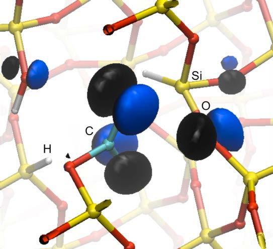
 by using first-principles calculations. SiO 2 C H")
34 Purpose We investigated the energetics, geometry, and electronic structures of C-substituted SiO 2 under wet oxidation conditions (H insertion) by using first-principles calculations. SiO 2 C H
35 (a) Calculation model of bulk SiO 2 (b) O O H C Si C S i -A inserted Carbon atom replace a Si atom in SiO 2. -Carbon atom and H atom is (a) inserted or (b) not inserted into 72 atoms alpha quartz.
36 Calculation method - First-principles calculations(gga) - Ultrasoft pseudo potential - Plane wave expansion - Cutoff energy 64 (Ryd.) - Sample k points 2x2x2 - Force convergence 10-3 ( Ht./a.u.)
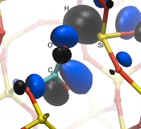
37 Results of C,H atom inserted in SiO 2 (Y. Ebihara et al. ISSS5 Tokyo (2011)) Si O C Si H O 1.28 C C-O:1.43Å C=O:1.23 Å C-O(carbonate) :1.29 Å (a) Only C atom was inserted (0 state) VT(SiC) CB(SiC) (b) C,H atom were inserted (-1 state) VT(SiC) CB(SiC) Si ー O O C O O ー :-2 C ー :-1 O O Si O O C O :0 Si Formation energy for (c) only C atom was inserted (d) C, H atom were inserted -Carbonate-like ion was created in SiO 2 which a C, O and H atom was inserted. -Therefore, negative charge state was most stable in SiC band gap. -C takes intrinsically preferred sp 2 network in SiO 2 assisted by the H atom.


38 Results: C and H atom incorporated in SiO 2 C O C O Si Si CB Wave function of O lone pare VT Si O C Si O C Si O C Energy level at Γ point. C, H atom inserted. Red line shows Fermi level Wave function of CO 3 like anti-bonding -We found that carbonate-like anti-bonding state and O lone pare state was formed in the SiO 2 band gap.

39 Results: C incorporation with 3H atoms O C H Si Calculation model for bulk SiO 2 where a C atom and three H atoms were inserted
 C,")
 CB(SiC) C, additional H atom")


40 Results: C incorporation with 3H atoms C, additional H atom inserted (0 state) C, additional H atom inserted (-1 state) VT(SiC) CB(SiC) C, additional H atom inserted (-2 state) Formation energy Negatively charged pseudo carbonate ions are generated by the assist of H atoms. Agreement with large Vfb shift by wet oxidation (Yano et al).


41 Results: C incorporation with 3H atoms Energy level at Γ point. C, H atom inserted. Wave function of CO 3 like Only Energy Level composed of pseudo CO3 ions are shown.
42 Summary of SiC 1. We found that C takes intrinsically preferred sp 2 network in SiO Especially, a carbonate-like ion is found to be formed in SiO 2 assisted by H. 3. These factors lead to the unexpected increase of flatband voltage shift and density of interface trap. The present study provides a knowlege to design and to improve practical fabrication of high quality SiC/SiO 2 interface.
43 Summary Computational science can predict and propose useful guiding principles of future nano-devices. (1) Operation mechanism of ReRAM, (2) Physical origin of negative fixed charge in SiC-MOSFET, and etc. can really be obtained by using computational science.
44 1. Introduction Contents 2. Key physics in ionic materials obtained by computational sciences. 3. Operation Mechanism of ReRAM 4. Physical Origin of Negative Fixed Charge by SiC Oxidation 5. Interface physics in high-k gate stacks 6. Summary 44
45 5. Interface physics in high-k gate stacks Energy gain (loss) when HfO 2 is in contact with Si E C E F E V E(Vo) 0.4eV 1.1eV (a) (b) HfO 2 E C E F E V E(Vo) 0.4eV 1.1eV HfO 2 poly-sigate 0 ev Hf-O bond is much stronger than Si-O bond->si cannot reduces HfO2 Formation enthalpy: 11.6eV(HfO2), 9.4eV(SiO2) poly-sigate SiO 2 V O ev Energy loss obtained by computational science When electrons occupy Vo level 45 and Vo is neutral (same as bulk)
46 Change in O ion form induces unexpected flat-band shift Y. Akasaka et al. Jpn. J. Appl. Phys J. Robertson, O. Sharia, and A. A. Demkov,APL 2007 (including image charge) P.Broqvist et al. APL 2008 (Including amorphous effect) E F metal Energy gain by electron transfer G 2 HfO2 Vo I L Si Reduction by Si sub. -G 1 HfO2 +1/2 Si (HfO2+Vo 2+ +2e)+1/2 SiO2 46
47 Change in O ion form induces unexpected flat-band shift E F metal Energy gain by electron transfer G 2 HfO2 Vo I L Si Reaction with Si sub. G 1 E F E F elevation metal + + Vo HfO2 I L Si Pinning position of a metal gate is defined by G1-G2=0: The reaction at Si/HfO2 interface governs the work function of a metal 47 under thermal equilibrium (Not metal/hfo2 interface. Gate first processes).
48 Change in O ion form induces unexpected flat-band shift E F metal Energy gain by electron transfer G 2 HfO2 Vo I L Si Reaction with Si sub. G 1 E F E F elevation metal + + Vo HfO2 I L Si Thermodynamics of interface reaction governs the FLP position HfO2 + ½ Si (HfO2 + Vo e) + ½ SiO2 48
49 Famous FLP occurs, and a metal WF is independent of metal species nor metal thickness 1.2 p+poly metal Vfb (p+) - Vfb (n+) (V) 1 Experiments [3] 0.8 This Thieory work Hafnia Thickness (ML) C. Hobbs et al. VLSI 2003 (Theory, K. Shiraishi et al VLSI 2004) M. Kadoshima et al. VLSI
50 Summary of mechanism of Fermi level pinning of poly-si gate Vo formation in ionic HfO 2 and subsequent electron transfer across the gate/dielectric interface generate large interface dipole. This is the basic origin of large flat band shift (Fermi level pinning). Development of metal gates is necessary. Capacitance (µf/cm 2 ) SiONnFET (p-well) 2 n+gate p+gate Voltage (V) Capacitance (µf/cm 2 ) HfAlOx nfet (p-well) 2 n+gate p+gate Voltage (V) Capacitance (µf/cm 2 ) HfSiOx nfet (p-well) 2 n+gate 1 0 p+gate Voltage (V) 50
51 Differences between poly-si gates and metal gates when IL is thin. e - transfer O transfer Poly-Si Poly-Si with cap layer p-metal occur occur Vo 2 + occur very small p + poly-si 2 HfO 2 Si sub. not occur occur very small p + poly barrier HfO 2 Si sub. not occur Vo 2 + Vo 2 + occur occur occur very small p-metal HfO 2 Si sub. Substrate reaction (HfO 2 ) + ½ Si (HfO 2 ) + Vo e + ½SiO 2 occurs in every case. This reaction is the same as poly-si gate reaction. (HfO 2 ) + ½ Si (HfO 2 ) + Vo e + ½SiO 2 51
52 FLP recovery by O injection It is known that O injection can recover FLP (E. Cartier,VLSI 2005) E F (a) EF elevation metal Vo Energy gain by Semiconductor electron transfer G 2 (Si) Reaction with Si sub. HfSiON - G 1 E F (b) EF elevation metal HfSiON Vo O injection by ozone at RT A. Ohta et al., IWDTF
53 FLP recovery by O injection It is known that O injection can recover FLP (E. Cartier,VLSI 2005) E F (a) EF elevation metal Vo Energy gain by Semiconductor electron transfer G 2 (Si) Reaction with Si sub. HfSiON - G 1 E F (b) metal HfSiON Vo O injection by ozone at RT A. Ohta et al., IWDTF
54 Summary Computational science can predict and propose useful guiding principles of future nano-devices. (1) Operation mechanism of ReRAM, (2) Physical origin of negative fixed charge in SiC-MOSFET, and etc. can really be obtained by using computational science.
55 1. Introduction Contents 2. Key physics in ionic materials obtained by computational sciences. 3. Operation Mechanism of ReRAM 4. Physical Origin of Negative Fixed Charge by SiC Oxidation 5. Interface physics in high-k gate stacks 6. Guiding Principles toward high quality MONOS. 7. Summary 55
56 Basic MONOS structures O-incorporation into SiN layers is experimentally reported SiO 2 SiN SiO 2 :O atoms M. Miura, et al., IEICE Technical Report SDM There are lots of O atoms in SiO 2 /SiN interfaces. Effects of O- incorporation should be investigated for 56 realization of high quality MONOS.

57 Calculation model One substitutional O atom at N site Two substitutional O atoms at N sites nearest to the Si atom O Si O N Si N Taking into account the O- incorporation, we investigated two types of O-incorporated defect. 57
58 The calculation of P/E operation Program e - Erase e - We investigated atomic and electronic structural changes during Program/Erase operations (carrier injection & removal). 58


59 Most stable structure of each defect One substitutional O atom Two substitutional O atoms N O Si O Si Si atoms four-fold O atom three-fold coordinated Si atoms four-fold O atoms two-fold 59 coordinated
60 Many meta-stable states appear by P/E & thermal activation (investigating 2 O model) Bond reconstruction, Irreversible change 60
61 Many meta-stable states appear by P/E & thermal activation There is a path which cause local collapse 61
 P/E & Thermal Activation P/E Barrier is about 0.")

62 The collapse is caused by P/E & thermal activation with low barrier (~0.1eV) P/E & Thermal Activation P/E Barrier is about 0.1 ev coordination number of O atoms changes! Coordination number of O atoms is changed by P/E & thermal activation. Long movement of O atoms Local collapse of SiN layers 62
63 Proposal The Ideal Memory Structure of MONOS O atoms are charge traps, but irreversible!! O-incorporation should be suppressed The number of charge trap should be maintained e O e O SiO2 e O e O SiN SiO
64 For lowering µ Ο, our proposal is inserting a thin Si layer into SiO 2 SiN SiN µ(o) is higher Si SiO 2 µ(o) is lower Si SiO 2 Bad Retention (Large Leakage) Placed Si within SiN/SiO 2 interface can lower µ Ο One method is decrease the SiO 2 thickness A thin SiO 2 layer reduces the retention character 64 of a MONOS type memory.
65 For lowering µ Ο, our proposal is inserting a thin Si layer into SiO 2 SiN SiN µ(o) is higher Si SiO 2 µ(o) is lower Si SiO 2 Bad Retention (Large Leakage) Placed Si within SiN/SiO 2 interface can lower µ Ο One method is decrease the SiO 2 thickness A thin SiO 2 layer reduces the retention character 65 of a MONOS type memory.

66 For lowering µ Ο, our proposal is inserting a thin Si layer into SiO 2 Si SiN SiO 2 SiN SiO 2 Si SiN µ(o) is lowered Si Good Retention Si SiO 2 Our proposal recipe is Insertion of a thin Si layer into a SiO 2 layer near the SiN/SiO 2. This recipe realizes short distance between 66 Si/SiO 2 and SiO 2 /SiN with good retention.
 SiO 2 SiO 2 SiN Lower μ O SiN SiO 2 O atoms Si dots Suppression of O-incorporation SiO 2 K. Yamaguchi et al.")
67 Insertion of Si nano-dots or nano-wire Fabrication processes of SiO 2 with self-limiting oxidation of Si dots & nano-wire are effective. S. Horiguchi et al., Japan. J. Appl. Phys. 40, L29 (2001) SiO 2 SiO 2 SiN Lower μ O SiN SiO 2 O atoms Si dots Suppression of O-incorporation SiO 2 K. Yamaguchi et al. IEDM 2010 It is a common guiding principle to synthesize the sharp and high quality oxide interfaces. 67
68 Summary Computational science can predict and propose useful guiding principles of future nano-devices. Interface physics of high-k gate stacks, operation mechanism of ReRAM, guideline of high-endurance MONOS, etc., can really be obtained by using computational science.
69 Other experiments for new interface physics concept Y. Kamimuta et al. SSDM 2005 occur occur e Vo 2+ O occur occur very occur small FLP not occur small Vo 2+ occur occur very occur small FLP occur occur Vo 2+ occur not occur very occurl small FLP not occur small Vo 2+ occur not occur very small small No FLP p+poly HfO 2 Si sub. Interface reaction between HfO2 and Si is crucial 78
Defects in Semiconductors
 Defects in Semiconductors Mater. Res. Soc. Symp. Proc. Vol. 1370 2011 Materials Research Society DOI: 10.1557/opl.2011. 771 Electronic Structure of O-vacancy in High-k Dielectrics and Oxide Semiconductors
Control of Flat Band Voltage by Partial Incorporation of La 2 O 3 or Sc 2 O 3 into HfO 2 in Metal/HfO 2 /SiO 2 /Si MOS Capacitors
 Control of Flat Band Voltage by Partial Incorporation of La 2 O 3 or Sc 2 O 3 into HfO 2 in Metal/HfO 2 /SiO 2 /Si MOS Capacitors M. Adachi 1, K. Okamoto 1, K. Kakushima 2, P. Ahmet 1, K. Tsutsui 2, N.
ECE 340 Lecture 39 : MOS Capacitor II
 ECE 340 Lecture 39 : MOS Capacitor II Class Outline: Effects of Real Surfaces Threshold Voltage MOS Capacitance-Voltage Analysis Things you should know when you leave Key Questions What are the effects
MSE 310/ECE 340: Electrical Properties of Materials Fall 2014 Department of Materials Science and Engineering Boise State University
 MSE 310/ECE 340: Electrical Properties of Materials Fall 2014 Department of Materials Science and Engineering Boise State University Practice Final Exam 1 Read the questions carefully Label all figures
ESE 570: Digital Integrated Circuits and VLSI Fundamentals
 ESE 570: Digital Integrated Circuits and VLSI Fundamentals Lec 4: January 23, 2018 MOS Transistor Theory, MOS Model Penn ESE 570 Spring 2018 Khanna Lecture Outline! CMOS Process Enhancements! Semiconductor
Atomic configuration of boron pile-up at the Si/SiO 2 interface
 Atomic configuration of boron pile-up at the Si/SiO 2 interface Masayuki Furuhashi, a) Tetsuya Hirose, Hiroshi Tsuji, Masayuki Tachi, and Kenji Taniguchi Department of Electronics and Information Systems,
ESE370: Circuit-Level Modeling, Design, and Optimization for Digital Systems
 ESE370: Circuit-Level Modeling, Design, and Optimization for Digital Systems Lec 6: September 14, 2015 MOS Model You are Here: Transistor Edition! Previously: simple models (0 and 1 st order) " Comfortable
Gate Carrier Injection and NC-Non- Volatile Memories
 Gate Carrier Injection and NC-Non- Volatile Memories Jean-Pierre Leburton Department of Electrical and Computer Engineering and Beckman Institute University of Illinois at Urbana-Champaign Urbana, IL 61801,
Optimization of the Dielectric Constant of a Blocking Dielectric in the Nonvolatile Memory Based on Silicon Nitride
 ISSN 8756-699, Optoelectronics, Instrumentation and Data Processing, 9, Vol. 45, No. 4, pp. 48 5. c Allerton Press, Inc., 9. Original Russian Text c Y. N. Novikov, V. A. Gritsenko, K. A. Nasyrov, 9, published
Characterization of Charge Trapping and Dielectric Breakdown of HfAlOx/SiON Dielectric Gate Stack
 Characterization of Charge Trapping and Dielectric Breakdown of HfAlOx/SiON Dielectric Gate Stack Y. Pei, S. Nagamachi, H. Murakami, S. Higashi, S. Miyazaki, T. Kawahara and K. Torii Graduate School of
Resonant photo-ionization of point defects in HfO 2 thin films observed by second-harmonic generation.
 Optics of Surfaces & Interfaces - VIII September 10 th, 2009 Resonant photo-ionization of point defects in HfO 2 thin films observed by second-harmonic generation. Jimmy Price and Michael C. Downer Physics
Electrical and Reliability Characteristics of RRAM for Cross-point Memory Applications. Hyunsang Hwang
 Electrical and Reliability Characteristics of RRAM for Cross-point Memory Applications Hyunsang Hwang Dept. of Materials Science and Engineering Gwangju Institute of Science and Technology (GIST), KOREA
! CMOS Process Enhancements. ! Semiconductor Physics. " Band gaps. " Field Effects. ! MOS Physics. " Cut-off. " Depletion.
 ESE 570: Digital Integrated Circuits and VLSI Fundamentals Lec 4: January 3, 018 MOS Transistor Theory, MOS Model Lecture Outline! CMOS Process Enhancements! Semiconductor Physics " Band gaps " Field Effects!
ESE 570: Digital Integrated Circuits and VLSI Fundamentals
 ESE 570: Digital Integrated Circuits and VLSI Fundamentals Lec 4: January 29, 2019 MOS Transistor Theory, MOS Model Penn ESE 570 Spring 2019 Khanna Lecture Outline! CMOS Process Enhancements! Semiconductor
! CMOS Process Enhancements. ! Semiconductor Physics. " Band gaps. " Field Effects. ! MOS Physics. " Cut-off. " Depletion.
 ESE 570: Digital Integrated Circuits and VLSI Fundamentals Lec 4: January 9, 019 MOS Transistor Theory, MOS Model Lecture Outline CMOS Process Enhancements Semiconductor Physics Band gaps Field Effects
Analysis of Band-to-band. Tunneling Structures. Title of Talk. Dimitri Antoniadis and Judy Hoyt (PIs) Jamie Teherani and Tao Yu (Students) 8/21/2012
 Jamie Teherani and Tao Yu (Students) 8/21/2012") 1 Analysis of Band-to-band Title of Talk Tunneling Structures Dimitri Antoniadis and Judy Hoyt (PIs) Jamie Teherani and Tao Yu (Students) 8/21/2012 A Science & Technology Center Vertical Type-II TFET Structure
1 Analysis of Band-to-band Title of Talk Tunneling Structures Dimitri Antoniadis and Judy Hoyt (PIs) Jamie Teherani and Tao Yu (Students) 8/21/2012 A Science & Technology Center Vertical Type-II TFET Structure
Influence of electrode materials on CeO x based resistive switching
 Influence of electrode materials on CeO x based resistive switching S. Kano a, C. Dou a, M. Hadi a, K. Kakushima b, P. Ahmet a, A. Nishiyama b, N. Sugii b, K. Tsutsui b, Y. Kataoka b, K. Natori a, E. Miranda
Quantum Mechanical Simulation for Ultra-thin High-k Gate Dielectrics Metal Oxide Semiconductor Field Effect Transistors
 Mechanical Simulation for Ultra-thin High-k Gate Dielectrics Metal Oxide Semiconductor Field Effect Transistors Shih-Ching Lo 1, Yiming Li 2,3, and Jyun-Hwei Tsai 1 1 National Center for High-Performance
! Previously: simple models (0 and 1 st order) " Comfortable with basic functions and circuits. ! This week and next (4 lectures)
 Comfortable with basic functions and circuits. ! This week and next (4 lectures)") ESE370: CircuitLevel Modeling, Design, and Optimization for Digital Systems Lec 6: September 14, 2015 MOS Model You are Here: Transistor Edition! Previously: simple models (0 and 1 st order) " Comfortable
ESE370: CircuitLevel Modeling, Design, and Optimization for Digital Systems Lec 6: September 14, 2015 MOS Model You are Here: Transistor Edition! Previously: simple models (0 and 1 st order) " Comfortable
Interface dipole engineering in metal gate/high-k stacks
 Review Condensed Matter Physics August 2012 Vol.57 No.22: 2872 2878 doi: 10.1007/s11434-012-5289-6 SPECIAL TOPICS: Interface dipole engineering in metal gate/high-k stacks HUANG AnPing 1*, ZHENG XiaoHu
ESE370: Circuit-Level Modeling, Design, and Optimization for Digital Systems
 ESE370: Circuit-Level Modeling, Design, and Optimization for Digital Systems Lec 6: September 18, 2017 MOS Model You are Here: Transistor Edition! Previously: simple models (0 and 1 st order) " Comfortable
J. Price, 1,2 Y. Q. An, 1 M. C. Downer 1 1 The university of Texas at Austin, Department of Physics, Austin, TX
 Understanding process-dependent oxygen vacancies in thin HfO 2 /SiO 2 stacked-films on Si (100) via competing electron-hole injection dynamic contributions to second harmonic generation. J. Price, 1,2
Size-dependent Metal-insulator Transition Random Materials Crystalline & Amorphous Purely Electronic Switching
 Nanometallic RRAM I-Wei Chen Department of Materials Science and Engineering University of Pennsylvania Philadelphia, PA 19104 Nature Nano, 6, 237 (2011) Adv Mater,, 23, 3847 (2011) Adv Func Mater,, 22,
+ V gate M O. Trend: As k, E g. Part 6: High Dielectric Constant (k), Gate Electrode, & Channel Materials. Bandgap versus Dielectric Constant (k) k k
, Gate Electrode, & Channel Materials. Bandgap versus Dielectric Constant (k) k k") Part 6: High Dielectric Constant (k), Gate Electrode, & Channel Materials O 2 gate oxide is approaching physical limits Thickness & Current M O S poly-crystalline V Source W Source Contact Insulator n
Part 6: High Dielectric Constant (k), Gate Electrode, & Channel Materials O 2 gate oxide is approaching physical limits Thickness & Current M O S poly-crystalline V Source W Source Contact Insulator n
ESE370: Circuit-Level Modeling, Design, and Optimization for Digital Systems. Today MOS MOS. Capacitor. Idea
 ESE370: Circuit-Level Modeling, Design, and Optimization for Digital Systems Day 9: September 26, 2011 MOS Model Today MOS Structure Basic Idea Semiconductor Physics Metals, insulators Silicon lattice
Moores Law for DRAM. 2x increase in capacity every 18 months 2006: 4GB
 MEMORY Moores Law for DRAM 2x increase in capacity every 18 months 2006: 4GB Corollary to Moores Law Cost / chip ~ constant (packaging) Cost / bit = 2X reduction / 18 months Current (2008) ~ 1 micro-cent
Theory of Hydrogen-Related Levels in Semiconductors and Oxides
 Theory of Hydrogen-Related Levels in Semiconductors and Oxides Chris G. Van de Walle Materials Department University of California, Santa Barbara Acknowledgments Computations J. Neugebauer (Max-Planck-Institut,
Surfaces, Interfaces, and Layered Devices
 Surfaces, Interfaces, and Layered Devices Building blocks for nanodevices! W. Pauli: God made solids, but surfaces were the work of Devil. Surfaces and Interfaces 1 Interface between a crystal and vacuum
High Dielectric Constant (k) Materials
 Materials") Part 6: High Dielectric Constant (k), Gate Electrode, & Channel Materials O 2 gate ide is approaching physical limits Thickness & Current M O S poly-crystalline V Source W Source Contact Insulator n +
Part 6: High Dielectric Constant (k), Gate Electrode, & Channel Materials O 2 gate ide is approaching physical limits Thickness & Current M O S poly-crystalline V Source W Source Contact Insulator n +
Energy position of the active near-interface traps in metal oxide semiconductor field-effect transistors on 4H SiC
 Energy position of the active near-interface traps in metal oxide semiconductor field-effect transistors on 4H SiC Author Haasmann, Daniel, Dimitrijev, Sima Published 2013 Journal Title Applied Physics
Semiconductor Physics fall 2012 problems
 Semiconductor Physics fall 2012 problems 1. An n-type sample of silicon has a uniform density N D = 10 16 atoms cm -3 of arsenic, and a p-type silicon sample has N A = 10 15 atoms cm -3 of boron. For each
Traps in MOCVD n-gan Studied by Deep Level Transient Spectroscopy and Minority Carrier Transient Spectroscopy
 Traps in MOCVD n-gan Studied by Deep Level Transient Spectroscopy and Minority Carrier Transient Spectroscopy Yutaka Tokuda Department of Electrical and Electronics Engineering, Aichi Institute of Technology,
MOS CAPACITOR AND MOSFET
 EE336 Semiconductor Devices 1 MOS CAPACITOR AND MOSFET Dr. Mohammed M. Farag Ideal MOS Capacitor Semiconductor Devices Physics and Technology Chapter 5 EE336 Semiconductor Devices 2 MOS Capacitor Structure
Application of High-κ Gate Dielectrics and Metal Gate Electrodes to enable Silicon and Non-Silicon Logic Nanotechnology
 Application of High-κ Gate Dielectrics and Metal Gate Electrodes to enable Silicon and Non-Silicon Logic Nanotechnology Robert Chau, Justin Brask, Suman Datta, Gilbert Dewey, Mark Doczy, Brian Doyle, Jack
Challenges and Opportunities. Prof. J. Raynien Kwo 年
 Nanoelectronics Beyond Si: Challenges and Opportunities Prof. J. Raynien Kwo 年 立 Si CMOS Device Scaling Beyond 22 nm node High κ,, Metal gates, and High mobility channel 1947 First Transistor 1960 1960
an introduction to Semiconductor Devices
 an introduction to Semiconductor Devices Donald A. Neamen Chapter 6 Fundamentals of the Metal-Oxide-Semiconductor Field-Effect Transistor Introduction: Chapter 6 1. MOSFET Structure 2. MOS Capacitor -
Lecture 12: MOS Capacitors, transistors. Context
 Lecture 12: MOS Capacitors, transistors Context In the last lecture, we discussed PN diodes, and the depletion layer into semiconductor surfaces. Small signal models In this lecture, we will apply those
ATOMIC-SCALE THEORY OF RADIATION-INDUCED PHENOMENA
 ATOMIC-SCALE THEORY OF RADIATION-INDUCED PHENOMENA OVERVIEW OF THE LAST FIVE YEARS AND NEW RESULTS Sokrates T. Pantelides Department of Physics and Astronomy, Vanderbilt University, Nashville, TN The theory
An interfacial investigation of high-dielectric constant material hafnium oxide on Si substrate B
 Thin Solid Films 488 (2005) 167 172 www.elsevier.com/locate/tsf An interfacial investigation of high-dielectric constant material hafnium oxide on Si substrate B S.C. Chen a, T, J.C. Lou a, C.H. Chien
Electrostatics of Nanowire Transistors
 Electrostatics of Nanowire Transistors Jing Guo, Jing Wang, Eric Polizzi, Supriyo Datta and Mark Lundstrom School of Electrical and Computer Engineering Purdue University, West Lafayette, IN, 47907 ABSTRACTS
Electrical Characteristics of MOS Devices
 Electrical Characteristics of MOS Devices The MOS Capacitor Voltage components Accumulation, Depletion, Inversion Modes Effect of channel bias and substrate bias Effect of gate oide charges Threshold-voltage
! Previously: simple models (0 and 1 st order) " Comfortable with basic functions and circuits. ! This week and next (4 lectures)
 Comfortable with basic functions and circuits. ! This week and next (4 lectures)") ESE370: CircuitLevel Modeling, Design, and Optimization for Digital Systems Lec 6: September 18, 2017 MOS Model You are Here: Transistor Edition! Previously: simple models (0 and 1 st order) " Comfortable
ESE370: CircuitLevel Modeling, Design, and Optimization for Digital Systems Lec 6: September 18, 2017 MOS Model You are Here: Transistor Edition! Previously: simple models (0 and 1 st order) " Comfortable
Organic Electronic Devices
 Organic Electronic Devices Week 5: Organic Light-Emitting Devices and Emerging Technologies Lecture 5.5: Course Review and Summary Bryan W. Boudouris Chemical Engineering Purdue University 1 Understanding
Semi-insulating SiC substrates for high frequency devices
 Klausurtagung Silberbach, 19. - 21. Feb. 2002 Institut für Werkstoffwissenschaften - WW 6 Semi-insulating SiC substrates for high frequency devices Vortrag von Matthias Bickermann Semi-insulating SiC substrates
The effect of point defects in zircon
 aterials for nuclear waste immobilization: The effect of point defects in zircon iguel Pruneda Department of Earth Sciences University of Centre for Ceramic Immobilisation Radiation damage process α-decay
EE143 Fall 2016 Microfabrication Technologies. Evolution of Devices
 EE143 Fall 2016 Microfabrication Technologies Prof. Ming C. Wu wu@eecs.berkeley.edu 511 Sutardja Dai Hall (SDH) 1-1 Evolution of Devices Yesterday s Transistor (1947) Today s Transistor (2006) 1-2 1 Why
UNIVERSITY OF CALIFORNIA College of Engineering Department of Electrical Engineering and Computer Sciences. EECS 130 Professor Ali Javey Fall 2006
 UNIVERSITY OF CALIFORNIA College of Engineering Department of Electrical Engineering and Computer Sciences EECS 130 Professor Ali Javey Fall 2006 Midterm 2 Name: SID: Closed book. Two sheets of notes are
Effects of Antimony Near SiO 2 /SiC Interfaces
 Effects of Antimony Near SiO 2 /SiC Interfaces P.M. Mooney, A.F. Basile, and Zenan Jiang Simon Fraser University, Burnaby, BC, V5A1S6, Canada and Yongju Zheng, Tamara Isaacs-Smith Smith, Aaron Modic, and
Electronic structure of transition metal high-k dielectrics: interfacial band offset energies for microelectronic devices
 Applied Surface Science 212 213 (2003) 563 569 Electronic structure of transition metal high-k dielectrics: interfacial band offset energies for microelectronic devices Gerald Lucovsky *, Gilbert B. Rayner
A Novel Flat Band Voltage Tuning for Metal/High-k Gate Stack Structure
 Master thesis 2008 A Novel Flat Band Voltage Tuning for Metal/High-k Gate Stack Structure Supervisor Professor Hiroshi Iwai Department of Electronics and Applied Physics Interdisciplinary Graduate School
Foster, Adam; Lopez Gejo, F.; Shluger, A. L.; Nieminen, Risto Vacancy and interstitial defects in hafnia
 Powered by TCPDF (www.tcpdf.org) This is an electronic reprint of the original article. This reprint may differ from the original in pagination and typographic detail. Foster, Adam; Lopez Gejo, F.; Shluger,
Fabrication Technology, Part I
 EEL5225: Principles of MEMS Transducers (Fall 2004) Fabrication Technology, Part I Agenda: Microfabrication Overview Basic semiconductor devices Materials Key processes Oxidation Thin-film Deposition Reading:
Scaling Issues in Planar FET: Dual Gate FET and FinFETs
 Scaling Issues in Planar FET: Dual Gate FET and FinFETs Lecture 12 Dr. Amr Bayoumi Fall 2014 Advanced Devices (EC760) Arab Academy for Science and Technology - Cairo 1 Outline Scaling Issues for Planar
1 Name: Student number: DEPARTMENT OF PHYSICS AND PHYSICAL OCEANOGRAPHY MEMORIAL UNIVERSITY OF NEWFOUNDLAND. Fall :00-11:00
 1 Name: DEPARTMENT OF PHYSICS AND PHYSICAL OCEANOGRAPHY MEMORIAL UNIVERSITY OF NEWFOUNDLAND Final Exam Physics 3000 December 11, 2012 Fall 2012 9:00-11:00 INSTRUCTIONS: 1. Answer all seven (7) questions.
Characterization of reliability-limiting defects in 4H-SiC MOSFETs using density functional (atomistic) simulations
 simulations") Characterization of reliability-limiting defects in 4H-SiC MOSFETs using density functional (atomistic) simulations Dev Ettisserry ARL Workshop 14, 15 August, 2014 UMD, College Park Advised by : Prof.
Characterization of reliability-limiting defects in 4H-SiC MOSFETs using density functional (atomistic) simulations Dev Ettisserry ARL Workshop 14, 15 August, 2014 UMD, College Park Advised by : Prof.
Stretching the Barriers An analysis of MOSFET Scaling. Presenters (in order) Zeinab Mousavi Stephanie Teich-McGoldrick Aseem Jain Jaspreet Wadhwa
 Zeinab Mousavi Stephanie Teich-McGoldrick Aseem Jain Jaspreet Wadhwa") Stretching the Barriers An analysis of MOSFET Scaling Presenters (in order) Zeinab Mousavi Stephanie Teich-McGoldrick Aseem Jain Jaspreet Wadhwa Why Small? Higher Current Lower Gate Capacitance Higher
Stretching the Barriers An analysis of MOSFET Scaling Presenters (in order) Zeinab Mousavi Stephanie Teich-McGoldrick Aseem Jain Jaspreet Wadhwa Why Small? Higher Current Lower Gate Capacitance Higher
Lecture 7: Extrinsic semiconductors - Fermi level
 Lecture 7: Extrinsic semiconductors - Fermi level Contents 1 Dopant materials 1 2 E F in extrinsic semiconductors 5 3 Temperature dependence of carrier concentration 6 3.1 Low temperature regime (T < T
EECS143 Microfabrication Technology
 EECS143 Microfabrication Technology Professor Ali Javey Introduction to Materials Lecture 1 Evolution of Devices Yesterday s Transistor (1947) Today s Transistor (2006) Why Semiconductors? Conductors e.g
Lecture Outline. ESE 570: Digital Integrated Circuits and VLSI Fundamentals. Review: MOSFET N-Type, P-Type. Semiconductor Physics.
 ESE 57: Digital Integrated Circuits and VLSI Fundamentals Lec 4: January 24, 217 MOS Transistor Theory, MOS Model Lecture Outline! Semiconductor Physics " Band gaps " Field Effects! MOS Physics " Cutoff
Section 12: Intro to Devices
 Section 12: Intro to Devices Extensive reading materials on reserve, including Robert F. Pierret, Semiconductor Device Fundamentals Bond Model of Electrons and Holes Si Si Si Si Si Si Si Si Si Silicon
ESE 570: Digital Integrated Circuits and VLSI Fundamentals
 ESE 570: Digital Integrated Circuits and VLSI Fundamentals Lec 4: January 24, 2017 MOS Transistor Theory, MOS Model Penn ESE 570 Spring 2017 Khanna Lecture Outline! Semiconductor Physics " Band gaps "
Semiconductor Devices, Fall Gunnar Malm, Associate Professor Integrated Devices and Circuits, Kista Campus
 Semiconductor Devices, Fall 2014 Gunnar Malm, Associate Professor Integrated Devices and Circuits, Kista Campus gunta@kth.se, 08-790 4332 Semiconductor procesing at KTH Electrum Laboratory Stepper Lithography
Class 05: Device Physics II
 Topics: 1. Introduction 2. NFET Model and Cross Section with Parasitics 3. NFET as a Capacitor 4. Capacitance vs. Voltage Curves 5. NFET as a Capacitor - Band Diagrams at V=0 6. NFET as a Capacitor - Accumulation
Temperature dependence of spin diffusion length in silicon by Hanle-type spin. precession
 Temperature dependence of spin diffusion length in silicon by Hanle-type spin precession T. Sasaki 1,a), T. Oikawa 1, T. Suzuki 2, M. Shiraishi 3, Y. Suzuki 3, and K. Noguchi 1 SQ Research Center, TDK
EE130: Integrated Circuit Devices
 EE130: Integrated Circuit Devices (online at http://webcast.berkeley.edu) Instructor: Prof. Tsu-Jae King (tking@eecs.berkeley.edu) TA s: Marie Eyoum (meyoum@eecs.berkeley.edu) Alvaro Padilla (apadilla@eecs.berkeley.edu)
Numerical and experimental characterization of 4H-silicon carbide lateral metal-oxide-semiconductor field-effect transistor
 Numerical and experimental characterization of 4H-silicon carbide lateral metal-oxide-semiconductor field-effect transistor Siddharth Potbhare, a Neil Goldsman, b and Gary Pennington Department of Electrical
Current mechanisms Exam January 27, 2012
 Current mechanisms Exam January 27, 2012 There are four mechanisms that typically cause currents to flow: thermionic emission, diffusion, drift, and tunneling. Explain briefly which kind of current mechanisms
Low Frequency Noise in MoS 2 Negative Capacitance Field-effect Transistor
 Low Frequency Noise in MoS Negative Capacitance Field-effect Transistor Sami Alghamdi, Mengwei Si, Lingming Yang, and Peide D. Ye* School of Electrical and Computer Engineering Purdue University West Lafayette,
Study of dynamics of charge trapping in a-si:h/sin TFTs
 Study of dynamics of charge trapping in a-si:h/sin TFTs A.R.Merticaru, A.J.Mouthaan, F.G.Kuper University of Twente P.O.Box 217, 7500 AE Enschede Phone:+31 53 4892754 Fax: +31 53 4891034 E-mail: a.r.merticaru@el.utwente.nl
I-V characteristics model for Carbon Nanotube Field Effect Transistors
 International Journal of Engineering & Technology IJET-IJENS Vol:14 No:04 33 I-V characteristics model for Carbon Nanotube Field Effect Transistors Rebiha Marki, Chérifa Azizi and Mourad Zaabat. Abstract--
ALD high-k and higher-k integration on GaAs
 ALD high-k and higher-k integration on GaAs Ozhan Koybasi 1), Min Xu 1), Yiqun Liu 2), Jun-Jieh Wang 2), Roy G. Gordon 2), and Peide D. Ye 1)* 1) School of Electrical and Computer Engineering, Purdue University,
Semiconductor-Detectors
 Semiconductor-Detectors 1 Motivation ~ 195: Discovery that pn-- junctions can be used to detect particles. Semiconductor detectors used for energy measurements ( Germanium) Since ~ 3 years: Semiconductor
23.0 Review Introduction
 EE650R: Reliability Physics of Nanoelectronic Devices Lecture 23: TDDB: Measurement of bulk trap density Date: Nov 13 2006 Classnotes: Dhanoop Varghese Review: Nauman Z Butt 23.0 Review In the last few
DISTRIBUTION OF POTENTIAL BARRIER HEIGHT LOCAL VALUES AT Al-SiO 2 AND Si-SiO 2 INTERFACES OF THE METAL-OXIDE-SEMICONDUCTOR (MOS) STRUCTURES
 STRUCTURES") DISTRIBUTION OF POTENTIAL BARRIER HEIGHT LOCAL VALUES AT Al-SiO 2 AND Si-SiO 2 INTERFACES OF THE ETAL-OXIDE-SEICONDUCTOR (OS) STRUCTURES KRZYSZTOF PISKORSKI (kpisk@ite.waw.pl), HENRYK. PRZEWLOCKI Institute
DISTRIBUTION OF POTENTIAL BARRIER HEIGHT LOCAL VALUES AT Al-SiO 2 AND Si-SiO 2 INTERFACES OF THE ETAL-OXIDE-SEICONDUCTOR (OS) STRUCTURES KRZYSZTOF PISKORSKI (kpisk@ite.waw.pl), HENRYK. PRZEWLOCKI Institute
EECS130 Integrated Circuit Devices
 EECS130 Integrated Circuit Devices Professor Ali Javey 10/30/2007 MOSFETs Lecture 4 Reading: Chapter 17, 19 Announcements The next HW set is due on Thursday. Midterm 2 is next week!!!! Threshold and Subthreshold
Formation of unintentional dots in small Si nanostructures
 Superlattices and Microstructures, Vol. 28, No. 5/6, 2000 doi:10.1006/spmi.2000.0942 Available online at http://www.idealibrary.com on Formation of unintentional dots in small Si nanostructures L. P. ROKHINSON,
Review of Semiconductor Physics. Lecture 3 4 Dr. Tayab Din Memon
 Review of Semiconductor Physics Lecture 3 4 Dr. Tayab Din Memon 1 Electronic Materials The goal of electronic materials is to generate and control the flow of an electrical current. Electronic materials
Classification of Solids
 Classification of Solids Classification by conductivity, which is related to the band structure: (Filled bands are shown dark; D(E) = Density of states) Class Electron Density Density of States D(E) Examples
InGaAs Double-Gate Fin-Sidewall MOSFET
 InGaAs Double-Gate Fin-Sidewall MOSFET Alon Vardi, Xin Zhao and Jesús del Alamo Microsystems Technology Laboratories, MIT June 25, 214 Sponsors: Sematech, Technion-MIT Fellowship, and NSF E3S Center (#939514)
Analytical Modeling of Threshold Voltage for a. Biaxial Strained-Si-MOSFET
 Contemporary Engineering Sciences, Vol. 4, 2011, no. 6, 249 258 Analytical Modeling of Threshold Voltage for a Biaxial Strained-Si-MOSFET Amit Chaudhry Faculty of University Institute of Engineering and
in this web service Cambridge University Press
 High-k Materials Mat. Res. Soc. Symp. Proc. Vol. 670 2001 Materials Research Society Materials and Physical Properties of Novel High-k and Medium-k Gate Dielectrics Ran Liu, Stefan Zollner, Peter Fejes,
Quantification of Trap State Densities at High-k/III-V Interfaces
 Quantification of Trap State Densities at High-k/III-V Interfaces Roman Engel-Herbert*, Yoontae Hwang, and Susanne Stemmer Materials Department, University of California, Santa Barbara *now at Penn State
Review of Semiconductor Fundamentals
 ECE 541/ME 541 Microelectronic Fabrication Techniques Review of Semiconductor Fundamentals Zheng Yang (ERF 3017, email: yangzhen@uic.edu) Page 1 Semiconductor A semiconductor is an almost insulating material,
Advanced Flash and Nano-Floating Gate Memories
 Advanced Flash and Nano-Floating Gate Memories Mater. Res. Soc. Symp. Proc. Vol. 1337 2011 Materials Research Society DOI: 10.1557/opl.2011.1028 Scaling Challenges for NAND and Replacement Memory Technology
arxiv:cond-mat/ v1 [cond-mat.mtrl-sci] 4 Oct 2004
![arxiv:cond-mat/ v1 [cond-mat.mtrl-sci] 4 Oct 2004](/thumbs/74/70376725.jpg "arxiv:cond-mat/ v1 [cond-mat.mtrl-sci] 4 Oct 2004") The role of nitrogen related defects in high-k dielectric oxides: density functional studies arxiv:cond-mat/0410088v1 [cond-mat.mtrl-sci] 4 Oct 2004 J. L. Gavartin 1, A. S. Foster 2, G. I. Bersuker 3 and
The role of nitrogen related defects in high-k dielectric oxides: density functional studies arxiv:cond-mat/0410088v1 [cond-mat.mtrl-sci] 4 Oct 2004 J. L. Gavartin 1, A. S. Foster 2, G. I. Bersuker 3 and
Large Storage Window in a-sinx/nc-si/a-sinx Sandwiched Structure
 2017 Asia-Pacific Engineering and Technology Conference (APETC 2017) ISBN: 978-1-60595-443-1 Large Storage Window in a-sinx/nc-si/a-sinx Sandwiched Structure Xiang Wang and Chao Song ABSTRACT The a-sin
Lecture 6 PN Junction and MOS Electrostatics(III) Metal-Oxide-Semiconductor Structure
 Metal-Oxide-Semiconductor Structure") Lecture 6 PN Junction and MOS Electrostatics(III) Metal-Oxide-Semiconductor Structure Outline 1. Introduction to MOS structure 2. Electrostatics of MOS in thermal equilibrium 3. Electrostatics of MOS with
Lecture 6 PN Junction and MOS Electrostatics(III) Metal-Oxide-Semiconductor Structure Outline 1. Introduction to MOS structure 2. Electrostatics of MOS in thermal equilibrium 3. Electrostatics of MOS with
Fundamentals of the Metal Oxide Semiconductor Field-Effect Transistor
 Triode Working FET Fundamentals of the Metal Oxide Semiconductor Field-Effect Transistor The characteristics of energy bands as a function of applied voltage. Surface inversion. The expression for the
Semiconductor Polymer
 Semiconductor Polymer Organic Semiconductor for Flexible Electronics Introduction: An organic semiconductor is an organic compound that possesses similar properties to inorganic semiconductors with hole
Indium arsenide quantum wire trigate metal oxide semiconductor field effect transistor
 JOURNAL OF APPLIED PHYSICS 99, 054503 2006 Indium arsenide quantum wire trigate metal oxide semiconductor field effect transistor M. J. Gilbert a and D. K. Ferry Department of Electrical Engineering and
Semiconductor Devices. C. Hu: Modern Semiconductor Devices for Integrated Circuits Chapter 5
 Semiconductor Devices C. Hu: Modern Semiconductor Devices for Integrated Circuits Chapter 5 Global leader in environmental and industrial measurement Wednesday 3.2. afternoon Tour around facilities & lecture
arxiv: v1 [cond-mat.mtrl-sci] 16 Apr 2009
![arxiv: v1 [cond-mat.mtrl-sci] 16 Apr 2009](/thumbs/93/112638923.jpg "arxiv: v1 [cond-mat.mtrl-sci] 16 Apr 2009") PRESAT-8401 First-Principles Study for Evidence of Low Interface Defect Density at Ge/GeO 2 Interfaces Shoichiro Saito, Takuji Hosoi, Heiji Watanabe, and Tomoya Ono arxiv:0904.2474v1 [cond-mat.mtrl-sci]
PRESAT-8401 First-Principles Study for Evidence of Low Interface Defect Density at Ge/GeO 2 Interfaces Shoichiro Saito, Takuji Hosoi, Heiji Watanabe, and Tomoya Ono arxiv:0904.2474v1 [cond-mat.mtrl-sci]
VSP A gate stack analyzer
 Microelectronics Reliability 47 (7) 74 78 www.elsevier.com/locate/microrel VSP A gate stack analyzer M. Karner *, A. Gehring, M. Wagner, R. Entner, S. Holzer, W. Goes, M. Vasicek, T. Grasser, H. Kosina,
Metal Semiconductor Contacts
 Metal Semiconductor Contacts The investigation of rectification in metal-semiconductor contacts was first described by Braun [33-35], who discovered in 1874 the asymmetric nature of electrical conduction
Solid State Device Fundamentals
 Solid State Device Fundamentals ENS 345 Lecture Course by Alexander M. Zaitsev alexander.zaitsev@csi.cuny.edu Tel: 718 982 2812 Office 4N101b 1 Outline - Goals of the course. What is electronic device?
C-V and G-V Measurements Showing Single Electron Trapping in Nanocrystalline Silicon Dot Embedded in MOS Memory Structure
 Mat. Res. Soc. Symp. Proc. Vol. 686 2002 Materials Research Society C-V and G-V Measurements Showing Single Electron Trapping in Nanocrystalline Silicon Dot Embedded in MOS Memory Structure Shaoyun Huang,
Semiconductors. Semiconductors also can collect and generate photons, so they are important in optoelectronic or photonic applications.
 Semiconductors Semiconducting materials have electrical properties that fall between true conductors, (like metals) which are always highly conducting and insulators (like glass or plastic or common ceramics)
Electrons, Holes, and Defect ionization
 Electrons, Holes, and Defect ionization The process of forming intrinsic electron-hole pairs is excitation a cross the band gap ( formation energy ). intrinsic electronic reaction : null e + h When electrons
MENA9510 characterization course: Capacitance-voltage (CV) measurements
 measurements") MENA9510 characterization course: Capacitance-voltage (CV) measurements 30.10.2017 Halvard Haug Outline Overview of interesting sample structures Ohmic and schottky contacts Why C-V for solar cells? The
MENA9510 characterization course: Capacitance-voltage (CV) measurements 30.10.2017 Halvard Haug Outline Overview of interesting sample structures Ohmic and schottky contacts Why C-V for solar cells? The
Semiconductor Physics Problems 2015
 Semiconductor Physics Problems 2015 Page and figure numbers refer to Semiconductor Devices Physics and Technology, 3rd edition, by SM Sze and M-K Lee 1. The purest semiconductor crystals it is possible