EE130: Integrated Circuit Devices
|
|
|
- Melvyn Simmons
- 5 years ago
- Views:
Transcription
1 EE130: Integrated Circuit Devices (online at Instructor: Prof. Tsu-Jae King TA s: Marie Eyoum Alvaro Padilla Web page: Newsgroup: ucb.class.ee130 Course Outline 1. Semiconductor Fundamentals 3 weeks 2. Metal-Semiconductor Contacts 1 week 3. P-N Junction Diode 3 weeks 4. Bipolar Junction Transistor 3 weeks 5. MOS Capacitor 1 week 6. MOSFET 4 weeks Gate Source Drain Substrate
2 Introduction Integrated-Circuit Devices Power4 µp 4004 µp

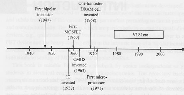
3 Planar Process Technology starting substrate + *planar processing steps = multiple devices monolithically integrated Si wafer n-channel MOSFET *sequence of additive and subtractive steps with lateral patterning oxidation deposition ion implantation etching lithography IC Technology Advancement Rapid advances in IC technology have been achieved primarily by scaling down transistor lateral dimensions Technology Scaling Investment Better Performance/Cost 100 ITRS 2001 Projection Market Growth GATE LENGTH (nm) 10 LOW POWER HIGH PERFORMANCE YEAR
4 Benefit of Transistor Scaling Moore s Law # transistors/chip doubles every 1.5 to 2 years 1,000,000, ,000,000 10,000,000 1,000, ,000 10, ,000 Example: Microprocessor Evolution Generation: 1.5µ 1.0µ 0.8µ 0.6µ 0.35µ 0.25µ Intel386 DX Processor Intel486 DX Processor Pentium Processor Pentium II Processor
5 Semiconductor Fundamentals OUTLINE General material properties Crystal structure Bond model Read: Chapter 1 What is a Semiconductor? Low resistivity => conductor High resistivity => insulator Intermediate resistivity => semiconductor conductivity lies between that of conductors and insulators generally crystalline in structure for IC devices In recent years, however, non-crystalline semiconductors have become commercially very important polycrystalline amorphous crystalline


6 Semiconductor Materials Elemental: Compound: Alloy: From Hydrogen to Silicon # of Electrons Z Name 1s 2s 2p 3s 3p 3d Notation 1H 1 1s 1 2He 2 1s 2 3Li 2 1 1s 2 2s 1 4Be 2 2 1s 2 2s 2 5 B s 2 2s 2 2p 1 6 C s 2 2s 2 2p 2 7 N s 2 2s 2 2p 3 8 O s 2 2s 2 2p 4 9 F s 2 2s 2 2p 5 10 Ne s 2 2s 2 2p 6 11 Na s 2 2s 2 2p 6 3s 1 12 Mg s 2 2s 2 2p 6 3s 2 13 Al s 2 2s 2 2p 6 3s 2 3p 1 14 Si s 2 2s 2 2p 6 3s 2 3p 2 15 P s 2 2s 2 2p 6 3s 2 3p 3 16 S s 2 2s 2 2p 6 3s 2 3p 4 17 Cl s 2 2s 2 2p 6 3s 2 3p 5 18 Ar s 2 2s 2 2p 6 3s 2 3p 6


7 The Silicon Atom 14 electrons occupying the 1st 3 energy levels: 1s, 2s, 2p orbitals filled by 10 electrons 3s, 3p orbitals filled by 4 electrons To minimize the overall energy, the 3s and 3p orbitals hybridize to form 4 tetrahedral 3sp orbitals Each has one electron and is capable of forming a bond with a neighboring atom The Si Crystal Each Si atom has 4 nearest neighbors lattice constant = 5.431Å diamond cubic lattice
8 Compound Semiconductors Ga As zincblende structure III-V compound semiconductors: GaAs, GaP, GaN, etc. important for optoelectronics and high-speed ICs Crystallographic Notation Miller Indices: Notation ( h k l ) { h k l } [ h k l ] < h k l > Interpretation crystal plane equivalent planes crystal direction equivalent directions h: inverse x-intercept of plane k: inverse y-intercept of plane l: inverse z-intercept of plane (Intercept values are in multiples of the lattice constant; h, k and l are reduced to 3 integers having the same ratio.)


 plane Crystallographic")


9 Crystallographic Planes and Si Wafers Silicon wafers are usually cut along the (100) plane with a flat or notch to orient the wafer during IC fabrication: (011) flat (100) plane Crystallographic Planes in Si Unit cell: lattice constant = 5.431Å 5 x atoms/cm 3 View in <111> direction View in <100> direction View in <110> direction
10 Electronic Properties of Si Silicon is a semiconductor material. Pure Si has a relatively high electrical resistivity at room temperature. There are 2 types of mobile charge-carriers in Si: Conduction electrons are negatively charged; Holes are positively charged. The concentration (#/cm 3 ) of conduction electrons & holes in a semiconductor can be modulated in several ways: 1. by adding special impurity atoms ( dopants ) 2. by applying an electric field 3. by changing the temperature 4. by irradiation Bond Model of Electrons and Holes Si Si Si 2-D representation: Si Si Si Si Si Si When an electron breaks loose and becomes a conduction electron, a hole is also created. Si Si Si Si Si Si Si Si Si
11 What is a Hole? Mobile positive charge associated with a half-filled covalent bond Treat as positively charged mobile particle in the semiconductor Fluid analogy: The Hole as a Positive Mobile Charge
12 Pure Si conduction n i cm -3 at room temperature Crystalline Si: Summary 4 valence electrons per atom diamond lattice: each atom has 4 nearest neighbors 5 x atoms/cm 3 In a pure Si crystal, conduction electrons and holes are formed in pairs. Holes can be considered as positively charged mobile particles which exist inside a semiconductor. Both holes and electrons can conduct current.
Semiconductor Device Physics
 1 Semiconductor Device Physics Lecture 1 http://zitompul.wordpress.com 2 0 1 3 2 Semiconductor Device Physics Textbook: Semiconductor Device Fundamentals, Robert F. Pierret, International Edition, Addison
Lecture 1. OUTLINE Basic Semiconductor Physics. Reading: Chapter 2.1. Semiconductors Intrinsic (undoped) silicon Doping Carrier concentrations
 silicon Doping Carrier concentrations") Lecture 1 OUTLINE Basic Semiconductor Physics Semiconductors Intrinsic (undoped) silicon Doping Carrier concentrations Reading: Chapter 2.1 EE105 Fall 2007 Lecture 1, Slide 1 What is a Semiconductor? Low
Lecture 1 OUTLINE Basic Semiconductor Physics Semiconductors Intrinsic (undoped) silicon Doping Carrier concentrations Reading: Chapter 2.1 EE105 Fall 2007 Lecture 1, Slide 1 What is a Semiconductor? Low
EECS143 Microfabrication Technology
 EECS143 Microfabrication Technology Professor Ali Javey Introduction to Materials Lecture 1 Evolution of Devices Yesterday s Transistor (1947) Today s Transistor (2006) Why Semiconductors? Conductors e.g
EE143 Fall 2016 Microfabrication Technologies. Evolution of Devices
 EE143 Fall 2016 Microfabrication Technologies Prof. Ming C. Wu wu@eecs.berkeley.edu 511 Sutardja Dai Hall (SDH) 1-1 Evolution of Devices Yesterday s Transistor (1947) Today s Transistor (2006) 1-2 1 Why
EE 5211 Analog Integrated Circuit Design. Hua Tang Fall 2012
 EE 5211 Analog Integrated Circuit Design Hua Tang Fall 2012 Today s topic: 1. Introduction to Analog IC 2. IC Manufacturing (Chapter 2) Introduction What is Integrated Circuit (IC) vs discrete circuits?
ESE370: Circuit-Level Modeling, Design, and Optimization for Digital Systems
 ESE370: Circuit-Level Modeling, Design, and Optimization for Digital Systems Lec 6: September 14, 2015 MOS Model You are Here: Transistor Edition! Previously: simple models (0 and 1 st order) " Comfortable
Fabrication Technology, Part I
 EEL5225: Principles of MEMS Transducers (Fall 2004) Fabrication Technology, Part I Agenda: Microfabrication Overview Basic semiconductor devices Materials Key processes Oxidation Thin-film Deposition Reading:
ESE370: Circuit-Level Modeling, Design, and Optimization for Digital Systems
 ESE370: Circuit-Level Modeling, Design, and Optimization for Digital Systems Lec 6: September 18, 2017 MOS Model You are Here: Transistor Edition! Previously: simple models (0 and 1 st order) " Comfortable
! Previously: simple models (0 and 1 st order) " Comfortable with basic functions and circuits. ! This week and next (4 lectures)
 Comfortable with basic functions and circuits. ! This week and next (4 lectures)") ESE370: CircuitLevel Modeling, Design, and Optimization for Digital Systems Lec 6: September 14, 2015 MOS Model You are Here: Transistor Edition! Previously: simple models (0 and 1 st order) " Comfortable
ESE370: CircuitLevel Modeling, Design, and Optimization for Digital Systems Lec 6: September 14, 2015 MOS Model You are Here: Transistor Edition! Previously: simple models (0 and 1 st order) " Comfortable
ESE370: Circuit-Level Modeling, Design, and Optimization for Digital Systems. Today MOS MOS. Capacitor. Idea
 ESE370: Circuit-Level Modeling, Design, and Optimization for Digital Systems Day 9: September 26, 2011 MOS Model Today MOS Structure Basic Idea Semiconductor Physics Metals, insulators Silicon lattice
Lecture 2. Semiconductor Physics. Sunday 4/10/2015 Semiconductor Physics 1-1
 Lecture 2 Semiconductor Physics Sunday 4/10/2015 Semiconductor Physics 1-1 Outline Intrinsic bond model: electrons and holes Charge carrier generation and recombination Intrinsic semiconductor Doping:
EE301 Electronics I , Fall
 EE301 Electronics I 2018-2019, Fall 1. Introduction to Microelectronics (1 Week/3 Hrs.) Introduction, Historical Background, Basic Consepts 2. Rewiev of Semiconductors (1 Week/3 Hrs.) Semiconductor materials
! Previously: simple models (0 and 1 st order) " Comfortable with basic functions and circuits. ! This week and next (4 lectures)
 Comfortable with basic functions and circuits. ! This week and next (4 lectures)") ESE370: CircuitLevel Modeling, Design, and Optimization for Digital Systems Lec 6: September 18, 2017 MOS Model You are Here: Transistor Edition! Previously: simple models (0 and 1 st order) " Comfortable
ESE370: CircuitLevel Modeling, Design, and Optimization for Digital Systems Lec 6: September 18, 2017 MOS Model You are Here: Transistor Edition! Previously: simple models (0 and 1 st order) " Comfortable
Semiconductor Physics and Devices
 Syllabus Advanced Nano Materials Semiconductor Physics and Devices Textbook Donald A. Neamen (McGraw-Hill) Semiconductor Physics and Devices Seong Jun Kang Department of Advanced Materials Engineering
Chapter 1 Overview of Semiconductor Materials and Physics
 Chapter 1 Overview of Semiconductor Materials and Physics Professor Paul K. Chu Conductivity / Resistivity of Insulators, Semiconductors, and Conductors Semiconductor Elements Period II III IV V VI 2 B
Introduction to Semiconductor Physics. Prof.P. Ravindran, Department of Physics, Central University of Tamil Nadu, India
 Introduction to Semiconductor Physics 1 Prof.P. Ravindran, Department of Physics, Central University of Tamil Nadu, India http://folk.uio.no/ravi/cmp2013 Review of Semiconductor Physics Semiconductor fundamentals
Section 12: Intro to Devices
 Section 12: Intro to Devices Extensive reading materials on reserve, including Robert F. Pierret, Semiconductor Device Fundamentals Bond Model of Electrons and Holes Si Si Si Si Si Si Si Si Si Silicon
Semiconductors. Semiconductors also can collect and generate photons, so they are important in optoelectronic or photonic applications.
 Semiconductors Semiconducting materials have electrical properties that fall between true conductors, (like metals) which are always highly conducting and insulators (like glass or plastic or common ceramics)
Chapter 12: Electrical Properties. RA l
 Charge carriers and conduction: Chapter 12: Electrical Properties Charge carriers include all species capable of transporting electrical charge, including electrons, ions, and electron holes. The latter
Crystal Properties. MS415 Lec. 2. High performance, high current. ZnO. GaN
 Crystal Properties Crystal Lattices: Periodic arrangement of atoms Repeated unit cells (solid-state) Stuffing atoms into unit cells Determine mechanical & electrical properties High performance, high current
Lecture 0: Introduction
 Lecture 0: Introduction Introduction q Integrated circuits: many transistors on one chip q Very Large Scale Integration (VLSI): bucketloads! q Complementary Metal Oxide Semiconductor Fast, cheap, low power
Solid State Device Fundamentals
 Solid State Device Fundamentals ENS 345 Lecture Course by Alexander M. Zaitsev alexander.zaitsev@csi.cuny.edu Tel: 718 982 2812 Office 4N101b 1 Outline - Goals of the course. What is electronic device?
FLCC Seminar. Spacer Lithography for Reduced Variability in MOSFET Performance
 1 Seminar Spacer Lithography for Reduced Variability in MOSFET Performance Prof. Tsu-Jae King Liu Electrical Engineering & Computer Sciences Dept. University of California at Berkeley Graduate Student:
Lecture 20: Semiconductor Structures Kittel Ch 17, p , extra material in the class notes
 Lecture 20: Semiconductor Structures Kittel Ch 17, p 494-503, 507-511 + extra material in the class notes MOS Structure Layer Structure metal Oxide insulator Semiconductor Semiconductor Large-gap Semiconductor
1 Review of semiconductor materials and physics
 Part One Devices 1 Review of semiconductor materials and physics 1.1 Executive summary Semiconductor devices are fabricated using specific materials that offer the desired physical properties. There are
ELEC311( 물리전자, Physical Electronics) Course Outlines:
 Course Outlines:") ELEC311( 물리전자, Physical Electronics) Course Outlines: by Professor Jung-Hee Lee Lecture notes are prepared with PPT and available before the class (http://abeek.knu.ac.kr). The topics in the notes are
ELEC311( 물리전자, Physical Electronics) Course Outlines: by Professor Jung-Hee Lee Lecture notes are prepared with PPT and available before the class (http://abeek.knu.ac.kr). The topics in the notes are
Electronic Devices & Circuits
 Electronic Devices & Circuits For Electronics & Communication Engineering By www.thegateacademy.com Syllabus Syllabus for Electronic Devices Energy Bands in Intrinsic and Extrinsic Silicon, Carrier Transport,
EECS130 Integrated Circuit Devices
 EECS130 Integrated Circuit Devices Professor Ali Javey 8/30/2007 Semiconductor Fundamentals Lecture 2 Read: Chapters 1 and 2 Last Lecture: Energy Band Diagram Conduction band E c E g Band gap E v Valence
Self-study problems and questions Processing and Device Technology, FFF110/FYSD13
 Self-study problems and questions Processing and Device Technology, FFF110/FYSD13 Version 2016_01 In addition to the problems discussed at the seminars and at the lectures, you can use this set of problems
LECTURE 23. MOS transistor. 1 We need a smart switch, i.e., an electronically controlled switch. Lecture Digital Circuits, Logic
 LECTURE 23 Lecture 16-20 Digital Circuits, Logic 1 We need a smart switch, i.e., an electronically controlled switch 2 We need a gain element for example, to make comparators. The device of our dreams
3C3 Analogue Circuits
 Department of Electronic & Electrical Engineering Trinity College Dublin, 2014 3C3 Analogue Circuits Prof J K Vij jvij@tcd.ie Lecture 1: Introduction/ Semiconductors & Doping 1 Course Outline (subject
Lecture 3b. Bonding Model and Dopants. Reading: (Cont d) Notes and Anderson 2 sections
 Notes and Anderson 2 sections") Lecture 3b Bonding Model and Dopants Reading: (Cont d) Notes and Anderson 2 sections 2.3-2.7 The need for more control over carrier concentration Without help the total number of carriers (electrons and
Lecture 3b Bonding Model and Dopants Reading: (Cont d) Notes and Anderson 2 sections 2.3-2.7 The need for more control over carrier concentration Without help the total number of carriers (electrons and
Lecture 2. Unit Cells and Miller Indexes. Reading: (Cont d) Anderson 2 1.8,
 Anderson 2 1.8,") Lecture 2 Unit Cells and Miller Indexes Reading: (Cont d) Anderson 2 1.8, 2.1-2.7 Unit Cell Concept The crystal lattice consists of a periodic array of atoms. Unit Cell Concept A building block that can
Lecture 2 Unit Cells and Miller Indexes Reading: (Cont d) Anderson 2 1.8, 2.1-2.7 Unit Cell Concept The crystal lattice consists of a periodic array of atoms. Unit Cell Concept A building block that can
Semiconductor physics I. The Crystal Structure of Solids
 Lecture 3 Semiconductor physics I The Crystal Structure of Solids 1 Semiconductor materials Types of solids Space lattices Atomic Bonding Imperfection and doping in SOLIDS 2 Semiconductor Semiconductors
Classification of Solids
 Classification of Solids Classification by conductivity, which is related to the band structure: (Filled bands are shown dark; D(E) = Density of states) Class Electron Density Density of States D(E) Examples
Basic Semiconductor Physics
 6 Basic Semiconductor Physics 6.1 Introduction With this chapter we start with the discussion of some important concepts from semiconductor physics, which are required to understand the operation of solar
Section 12: Intro to Devices
 Section 12: Intro to Devices Extensive reading materials on reserve, including Robert F. Pierret, Semiconductor Device Fundamentals EE143 Ali Javey Bond Model of Electrons and Holes Si Si Si Si Si Si Si
1 Name: Student number: DEPARTMENT OF PHYSICS AND PHYSICAL OCEANOGRAPHY MEMORIAL UNIVERSITY OF NEWFOUNDLAND. Fall :00-11:00
 1 Name: DEPARTMENT OF PHYSICS AND PHYSICAL OCEANOGRAPHY MEMORIAL UNIVERSITY OF NEWFOUNDLAND Final Exam Physics 3000 December 11, 2012 Fall 2012 9:00-11:00 INSTRUCTIONS: 1. Answer all seven (7) questions.
Lecture 1. Introduction to Electronic Materials. Reading: Pierret 1.1, 1.2, 1.4,
 Lecture 1 Introduction to Electronic Materials Reading: Pierret 1.1, 1.2, 1.4, 2.1-2.6 Atoms to Operational Amplifiers The goal of this course is to teach the fundamentals of non-linear circuit elements
A semiconductor is an almost insulating material, in which by contamination (doping) positive or negative charge carriers can be introduced.
 positive or negative charge carriers can be introduced.") Semiconductor A semiconductor is an almost insulating material, in which by contamination (doping) positive or negative charge carriers can be introduced. Page 2 Semiconductor materials Page 3 Energy levels
Semiconductor A semiconductor is an almost insulating material, in which by contamination (doping) positive or negative charge carriers can be introduced. Page 2 Semiconductor materials Page 3 Energy levels
Solid State Device Fundamentals
 Solid State Device Fundamentals ENS 345 Lecture Course by Alexander M. Zaitsev alexander.zaitsev@csi.cuny.edu Tel: 718 982 2812 Office 4N101b 1 Outline - Goals of the course. What is electronic device?
Semiconductor Devices, Fall Gunnar Malm, Associate Professor Integrated Devices and Circuits, Kista Campus
 Semiconductor Devices, Fall 2014 Gunnar Malm, Associate Professor Integrated Devices and Circuits, Kista Campus gunta@kth.se, 08-790 4332 Semiconductor procesing at KTH Electrum Laboratory Stepper Lithography
Review of Semiconductor Fundamentals
 ECE 541/ME 541 Microelectronic Fabrication Techniques Review of Semiconductor Fundamentals Zheng Yang (ERF 3017, email: yangzhen@uic.edu) Page 1 Semiconductor A semiconductor is an almost insulating material,
Chapter 4: Bonding in Solids and Electronic Properties. Free electron theory
 Chapter 4: Bonding in Solids and Electronic Properties Free electron theory Consider free electrons in a metal an electron gas. regards a metal as a box in which electrons are free to move. assumes nuclei
Review of Semiconductor Physics. Lecture 3 4 Dr. Tayab Din Memon
 Review of Semiconductor Physics Lecture 3 4 Dr. Tayab Din Memon 1 Electronic Materials The goal of electronic materials is to generate and control the flow of an electrical current. Electronic materials
Lecture 2 Electrons and Holes in Semiconductors
 EE 471: Transport Phenomena in Solid State Devices Spring 2018 Lecture 2 Electrons and Holes in Semiconductors Bryan Ackland Department of Electrical and Computer Engineering Stevens Institute of Technology
Quiz #1 Practice Problem Set
 Name: Student Number: ELEC 3908 Physical Electronics Quiz #1 Practice Problem Set? Minutes January 22, 2016 - No aids except a non-programmable calculator - All questions must be answered - All questions
ELECTRONIC I Lecture 1 Introduction to semiconductor. By Asst. Prof Dr. Jassim K. Hmood
 ELECTRONIC I Lecture 1 Introduction to semiconductor By Asst. Prof Dr. Jassim K. Hmood SOLID-STATE ELECTRONIC MATERIALS Electronic materials generally can be divided into three categories: insulators,
Nanoelectronics. Topics
 Nanoelectronics Topics Moore s Law Inorganic nanoelectronic devices Resonant tunneling Quantum dots Single electron transistors Motivation for molecular electronics The review article Overview of Nanoelectronic
Chapter 3 Basics Semiconductor Devices and Processing
 Chapter 3 Basics Semiconductor Devices and Processing Hong Xiao, Ph. D. www2.austin.cc.tx.us/hongxiao/book.htm Hong Xiao, Ph. D. www2.austin.cc.tx.us/hongxiao/book.htm 1 Objectives Identify at least two
EE495/695 Introduction to Semiconductors I. Y. Baghzouz ECE Department UNLV
 EE495/695 Introduction to Semiconductors I Y. Baghzouz ECE Department UNLV Introduction Solar cells have always been aligned closely with other electronic devices. We will cover the basic aspects of semiconductor
Chapter 2. Design and Fabrication of VLSI Devices
 Chapter 2 Design and Fabrication of VLSI Devices Jason Cong 1 Design and Fabrication of VLSI Devices Objectives: To study the materials used in fabrication of VLSI devices. To study the structure of devices
MOS Capacitors ECE 2204
 MOS apacitors EE 2204 Some lasses of Field Effect Transistors Metal-Oxide-Semiconductor Field Effect Transistor MOSFET, which will be the type that we will study in this course. Metal-Semiconductor Field
Electrons are shared in covalent bonds between atoms of Si. A bound electron has the lowest energy state.
 Photovoltaics Basic Steps the generation of light-generated carriers; the collection of the light-generated carriers to generate a current; the generation of a large voltage across the solar cell; and
Band Gap Engineering. Reading the Periodic Table and Understanding Optical and Electrical Properties in Semiconductors
 The Birnie Group solar class and website were created with much-appreciated support from the NSF CRCD Program under grants 0203504 and 0509886. Continuing Support from the McLaren Endowment is also greatly
Molecules and Condensed Matter
 Chapter 42 Molecules and Condensed Matter PowerPoint Lectures for University Physics, Thirteenth Edition Hugh D. Young and Roger A. Freedman Lectures by Wayne Anderson Goals for Chapter 42 To understand
From Last Time. Several important conceptual aspects of quantum mechanics Indistinguishability. Symmetry
 From Last Time Several important conceptual aspects of quantum mechanics Indistinguishability particles are absolutely identical Leads to Pauli exclusion principle (one Fermion / quantum state). Symmetry
electronics fundamentals
 electronics fundamentals circuits, devices, and applications THOMAS L. FLOYD DAVID M. BUCHLA Lesson 1: Diodes and Applications Semiconductors Figure 1-1 The Bohr model of an atom showing electrons in orbits
Make sure the exam paper has 9 pages (including cover page) + 3 pages of data for reference
 + 3 pages of data for reference") UNIVERSITY OF CALIFORNIA College of Engineering Department of Electrical Engineering and Computer Sciences Spring 2006 EE143 Midterm Exam #1 Family Name First name SID Signature Make sure the exam paper
UNIVERSITY OF CALIFORNIA College of Engineering Department of Electrical Engineering and Computer Sciences Spring 2006 EE143 Midterm Exam #1 Family Name First name SID Signature Make sure the exam paper
Lecture 15 OUTLINE. MOSFET structure & operation (qualitative) Review of electrostatics The (N)MOS capacitor
 Review of electrostatics The (N)MOS capacitor") Lecture 15 OUTLINE MOSFET structure & operation (qualitative) Review of electrostatics The (N)MOS capacitor Electrostatics t ti Charge vs. voltage characteristic Reading: Chapter 6.1 6.2.1 EE105 Fall 2007
Lecture 15 OUTLINE MOSFET structure & operation (qualitative) Review of electrostatics The (N)MOS capacitor Electrostatics t ti Charge vs. voltage characteristic Reading: Chapter 6.1 6.2.1 EE105 Fall 2007
EXTRINSIC SEMICONDUCTOR
 EXTRINSIC SEMICONDUCTOR In an extrinsic semiconducting material, the charge carriers originate from impurity atoms added to the original material is called impurity [or] extrinsic semiconductor. This Semiconductor
DO PHYSICS ONLINE ELECTRIC CURRENT FROM IDEAS TO IMPLEMENTATION ATOMS TO TRANSISTORS ELECTRICAL PROPERTIES OF SOLIDS
 DO PHYSICS ONLINE FROM IDEAS TO IMPLEMENTATION 9.4.3 ATOMS TO TRANSISTORS ELECTRICAL PROPERTIES OF SOLIDS ELECTRIC CURRENT Different substances vary considerably in their electrical properties. It is a
Week 13 MO Theory, Solids, & metals
 Week 13 MO Theory, Solids, & metals Q UEST IO N 1 Using the molecular orbital energy diagrams below, which one of the following diatomic molecules is LEAST likely to exist? A. Li2 B. Be2 C. B2 D. C2 E.
Semiconductor Physics fall 2012 problems
 Semiconductor Physics fall 2012 problems 1. An n-type sample of silicon has a uniform density N D = 10 16 atoms cm -3 of arsenic, and a p-type silicon sample has N A = 10 15 atoms cm -3 of boron. For each
smal band gap Saturday, April 9, 2011
 small band gap upper (conduction) band empty small gap valence band filled 2s 2p 2s 2p hybrid (s+p)band 2p no gap 2s (depend on the crystallographic orientation) extrinsic semiconductor semi-metal electron
Semiconductors. SEM and EDAX images of an integrated circuit. SEM EDAX: Si EDAX: Al. Institut für Werkstoffe der ElektrotechnikIWE
 SEM and EDAX images of an integrated circuit SEM EDAX: Si EDAX: Al source: [Cal 99 / 605] M&D-.PPT, slide: 1, 12.02.02 Classification semiconductors electronic semiconductors mixed conductors ionic conductors
EE236 Electronics. Computer and Systems Engineering Department. Faculty of Engineering Alexandria University. Fall 2014
 EE236 Electronics Computer and Systems Engineering Department Faculty of Engineering Alexandria University Fall 2014 Lecturer: Bassem Mokhtar, Ph.D. Assistant Professor Department of Electrical Engineering
Physical Properties of Materials. 1. Electrical Properties 2. Optical Properties 3. Magnetic Properties
 Physical Properties of Materials 1. Electrical Properties 2. Optical Properties 3. Magnetic Properties 1 1. electrical properties 2 (1) electrical conduction in metals classical Model metallic bonds make
Solids. properties & structure
 Solids properties & structure Determining Crystal Structure crystalline solids have a very regular geometric arrangement of their particles the arrangement of the particles and distances between them is
Bonding in solids The interaction of electrons in neighboring atoms of a solid serves the very important function of holding the crystal together.
 Bonding in solids The interaction of electrons in neighboring atoms of a solid serves the very important function of holding the crystal together. For example Nacl In the Nacl lattice, each Na atom is
David J. Starling Penn State Hazleton PHYS 214
 Being virtually killed by a virtual laser in a virtual space is just as effective as the real thing, because you are as dead as you think you are. -Douglas Adams, Mostly Harmless David J. Starling Penn
Chemistry Instrumental Analysis Lecture 8. Chem 4631
 Chemistry 4631 Instrumental Analysis Lecture 8 UV to IR Components of Optical Basic components of spectroscopic instruments: stable source of radiant energy transparent container to hold sample device
Lecture 15 OUTLINE. MOSFET structure & operation (qualitative) Review of electrostatics The (N)MOS capacitor
 Review of electrostatics The (N)MOS capacitor") Lecture 15 OUTLINE MOSFET structure & operation (qualitative) Review of electrostatics The (N)MOS capacitor Electrostatics Charge vs. voltage characteristic Reading: Chapter 6.1 6.2.1 EE15 Spring 28 Lecture
Lecture 15 OUTLINE MOSFET structure & operation (qualitative) Review of electrostatics The (N)MOS capacitor Electrostatics Charge vs. voltage characteristic Reading: Chapter 6.1 6.2.1 EE15 Spring 28 Lecture
Physics 156: Applications of Solid State Physics
 Physics 156: Applications of Solid State Physics Instructor: Sue Carter Office NSII 349 Office Hours: Wednesdays 11:30 to 1 pm or by appointment Email: sacarter@ucsc.edu Book: http://ece-www.colorado.edu/~bart/book/book/title.htm
Chap. 1 (Introduction), Chap. 2 (Components and Circuits)
, Chap. 2 (Components and Circuits)") CHEM 455 The class describes the principles and applications of modern analytical instruments. Emphasis is placed upon the theoretical basis of each type of instrument, its optimal area of application,
CHEM 455 The class describes the principles and applications of modern analytical instruments. Emphasis is placed upon the theoretical basis of each type of instrument, its optimal area of application,
Final Examination EE 130 December 16, 1997 Time allotted: 180 minutes
 Final Examination EE 130 December 16, 1997 Time allotted: 180 minutes Problem 1: Semiconductor Fundamentals [30 points] A uniformly doped silicon sample of length 100µm and cross-sectional area 100µm 2
Fundamentals of the Metal Oxide Semiconductor Field-Effect Transistor
 Triode Working FET Fundamentals of the Metal Oxide Semiconductor Field-Effect Transistor The characteristics of energy bands as a function of applied voltage. Surface inversion. The expression for the
UConn ECE 4211, Semiconductor Devices and Nanostructures Lecture Week 1 January 17, 2017
 UConn ECE 411, Semiconductor Devices and Nanostructures Lecture Week 1 January 17, 017 Device Operation: One of the objectives of this course is to understand operation of carrier transport in semiconductor
16EC401 BASIC ELECTRONIC DEVICES UNIT I PN JUNCTION DIODE. Energy Band Diagram of Conductor, Insulator and Semiconductor:
 16EC401 BASIC ELECTRONIC DEVICES UNIT I PN JUNCTION DIODE Energy bands in Intrinsic and Extrinsic silicon: Energy Band Diagram of Conductor, Insulator and Semiconductor: 1 2 Carrier transport: Any motion
Digital Electronics Part II - Circuits
 Digital Electronics Part - Circuits Dr.. J. Wassell Gates from Transistors ntroduction Logic circuits are non-linear, consequently we will introduce a graphical technique for analysing such circuits The
ESE 570: Digital Integrated Circuits and VLSI Fundamentals
 ESE 570: Digital Integrated Circuits and VLSI Fundamentals Lec 4: January 23, 2018 MOS Transistor Theory, MOS Model Penn ESE 570 Spring 2018 Khanna Lecture Outline! CMOS Process Enhancements! Semiconductor
ELEC 4700 Assignment #2
 ELEC 4700 Assignment #2 Question 1 (Kasop 4.2) Molecular Orbitals and Atomic Orbitals Consider a linear chain of four identical atoms representing a hypothetical molecule. Suppose that each atomic wavefunction
First-Hand Investigation: Modeling of Semiconductors
 perform an investigation to model the behaviour of semiconductors, including the creation of a hole or positive charge on the atom that has lost the electron and the movement of electrons and holes in
CLASS 12th. Semiconductors
 CLASS 12th Semiconductors 01. Distinction Between Metals, Insulators and Semi-Conductors Metals are good conductors of electricity, insulators do not conduct electricity, while the semiconductors have
Introduction to Engineering Materials ENGR2000. Dr.Coates
 Introduction to Engineering Materials ENGR2000 Chapter 18: Electrical Properties Dr.Coates 18.2 Ohm s Law V = IR where R is the resistance of the material, V is the voltage and I is the current. l R A
Physics and Material Science of Semiconductor Nanostructures
 Physics and Material Science of Semiconductor Nanostructures PHYS 570P Prof. Oana Malis Email: omalis@purdue.edu Course website: http://www.physics.purdue.edu/academic_programs/courses/phys570p/ 1 Introduction
FREQUENTLY ASKED QUESTIONS February 21, 2017
 FREQUENTLY ASKED QUESTIONS February 21, 2017 Content Questions How do you place a single arsenic atom with the ratio 1 in 100 million? Sounds difficult to get evenly spread throughout. Yes, techniques
Basic cell design. Si cell
 Basic cell design Si cell 1 Concepts needed to describe photovoltaic device 1. energy bands in semiconductors: from bonds to bands 2. free carriers: holes and electrons, doping 3. electron and hole current:
Session 6: Solid State Physics. Diode
 Session 6: Solid State Physics Diode 1 Outline A B C D E F G H I J 2 Definitions / Assumptions Homojunction: the junction is between two regions of the same material Heterojunction: the junction is between
MSE 310/ECE 340: Electrical Properties of Materials Fall 2014 Department of Materials Science and Engineering Boise State University
 MSE 310/ECE 340: Electrical Properties of Materials Fall 2014 Department of Materials Science and Engineering Boise State University Practice Final Exam 1 Read the questions carefully Label all figures
ESE 570: Digital Integrated Circuits and VLSI Fundamentals
 ESE 570: Digital Integrated Circuits and VLSI Fundamentals Lec 4: January 24, 2017 MOS Transistor Theory, MOS Model Penn ESE 570 Spring 2017 Khanna Lecture Outline! Semiconductor Physics " Band gaps "
The photovoltaic effect occurs in semiconductors where there are distinct valence and
 How a Photovoltaic Cell Works The photovoltaic effect occurs in semiconductors where there are distinct valence and conduction bands. (There are energies at which electrons can not exist within the solid)
Unit IV Semiconductors Engineering Physics
 Introduction A semiconductor is a material that has a resistivity lies between that of a conductor and an insulator. The conductivity of a semiconductor material can be varied under an external electrical
Chapter 1 Semiconductor basics
 Chapter 1 Semiconductor basics ELEC-H402/CH1: Semiconductor basics 1 Basic semiconductor concepts Semiconductor basics Semiconductors, silicon and hole-electron pair Intrinsic silicon properties Doped
INFORMATION ABOUT THE COURSE
 KOM2751 Analog Electronics :: Dr. Muharrem Mercimek :: YTU - Control and Automation Dept. 1 INFORMATION ABOUT THE COURSE KOM2751 Analog Electronics KOM2751 Analog Electronics :: Dr. Muharrem Mercimek ::
ELECTRONIC DEVICES AND CIRCUITS SUMMARY
 ELECTRONIC DEVICES AND CIRCUITS SUMMARY Classification of Materials: Insulator: An insulator is a material that offers a very low level (or negligible) of conductivity when voltage is applied. Eg: Paper,
Crystalline Solids. Amorphous Solids
 Crystal Structure Crystalline Solids Possess rigid and long-range order; atoms, molecules, or ions occupy specific positions the tendency is to maximize attractive forces Amorphous Solids lack long-range
CLASS 1 & 2 REVISION ON SEMICONDUCTOR PHYSICS. Reference: Electronic Devices by Floyd
 CLASS 1 & 2 REVISION ON SEMICONDUCTOR PHYSICS Reference: Electronic Devices by Floyd 1 ELECTRONIC DEVICES Diodes, transistors and integrated circuits (IC) are typical devices in electronic circuits. All
an introduction to Semiconductor Devices
 an introduction to Semiconductor Devices Donald A. Neamen Chapter 6 Fundamentals of the Metal-Oxide-Semiconductor Field-Effect Transistor Introduction: Chapter 6 1. MOSFET Structure 2. MOS Capacitor -
Electrical Characteristics of MOS Devices
 Electrical Characteristics of MOS Devices The MOS Capacitor Voltage components Accumulation, Depletion, Inversion Modes Effect of channel bias and substrate bias Effect of gate oide charges Threshold-voltage