+ V gate M O. Trend: As k, E g. Part 6: High Dielectric Constant (k), Gate Electrode, & Channel Materials. Bandgap versus Dielectric Constant (k) k k
|
|
|
- Charles Garrett
- 6 years ago
- Views:
Transcription


 37-85 1 Bandgap versus Dielectric Constant (k) Trend: As k, E g e E e Hik c e")
1 Part 6: High Dielectric Constant (k), Gate Electrode, & Channel Materials O 2 gate oxide is approaching physical limits Thickness & Current M O S poly-crystalline V Source W Source Contact Insulator n + source + V gate n ++ Poly Gate Contact or Electrode O 2 - Gate oxide channel p- Wafer Drain Contact Insulator n + drain V Drain + Crystalline L t ox C ox okoxa t ox t EOT k k t ox highk highk Frank, Dennard, Nowak, Soloman, Wong & Taur, Proc. IEEE Circuit & Devices, 89 (2001) 259 M. Houssa et al., Materials Science and Engineering R, 51 (2006) Bandgap versus Dielectric Constant (k) Trend: As k, E g e E e Hik c e e E Hik c Robertson, MRS Bulletin (March 2002) p. 217 Robertson, J. Vac. Sci. Technol. B, 18(3), May/Jun
2 Band Offsets: High k on Aspects to Consider: 1. E g 2. E c & E v 3. m eff Recall in Barrier Region: e So: kx J e * 2kx k k 2 m ( V E ) eff m eff e m, J eff e E e Hik c e e E Hik c Robertson, MRS Bulletin (March 2002) p. 217 J g ( kt ) k fleftde Ef frightde E f dk pˆ 1 E where p mg & g & g m k 3 Band diagrams of MOS compare O 2 to high k materials O 2 ; κ~3.9 HfO 2 ; κ~25 PbZr (0.53) Ti (0.47) O 3 κ~200 Low S/C doping Southwick &, IEEE TDMR, 6(2), (2006)
 of O 2. Why? Y 2 O 3 O 2 Al 2 O 3 G G O2 Y2O3 O more stable than Y O 2 2 3 R.")
3 Need to consider the Thermodynamics of the materials system Ellingham diagram G vs- Temperature The more negative G is, the more stable the materials system is. Example: Grow Y 2 O 3 on, will steal oxygen from Y 2 O 3 to form interfacial layer (IL) of O 2. Why? Y 2 O 3 O 2 Al 2 O 3 G G O2 Y2O3 O more stable than Y O R. DeHoff, Thermodynamics of Materials, (Prentice Hall, 1996) Ch. 11, fig Interfacial layer (IL) of O 2 Present for HfO 2 TiN 3.5 EOT WRT t O2 & t HfO2 3 O 2 IL HfO 2 E OT n m t IL Crystalline Channel t HfO2 nm k t t t IL ox, eff IL highk khighk 6 3
, (2006) 136-145 7 - NVM Floating Gate NVM Versus SONOS (O 2-3 N 4 -O 2 -) NVM SONOS Advantages over Floating Gate: Replace poly- floating gate with 3 N 4 Stored")
4 EOT: 7 nm HfO 2 & 1nm O 2 : EOT ~ 2 nm 8 nm HfO 2 : EOT ~ 1.25 nm Southwick &, IEEE TDMR, 6(2), (2006) NVM Floating Gate NVM Versus SONOS (O 2-3 N 4 -O 2 -) NVM SONOS Advantages over Floating Gate: Replace poly- floating gate with 3 N 4 Stored charge lies in defect (bound) states below 3 N 4 conduction band Improved endurance - single defect will not cause the discharge/leakage of carriers Can reduce Thickness of TO 3 N 4 thinner than floating gate Poly Carriers not Floating around Minimizes interaction with neighboring memory cells Thus, can scale down memory cell size BL BL = Blocking Layer CTL = Charge Trapping Layer TL = Tunnel Layer CTL TL Todd Wallinger, SONOS Eases Non-Volatile Memory Integration in SoC, Semiconductor International (2007) 8 4

 9 - NVM Flat Band Condition BL TL Poly 3 N 4")
 10 5")
5 - NVM BL CTL TL BL CTL TL BL TL Flat Band Condition Poly Floating Gate Poly Energy Band Diagram Energy Band Diagram 3 N 4 = CTL Gate stack scaled down in thickness & cell area Todd Wallinger, SONOS Eases Non-Volatile Memory Integration in SoC, Semiconductor International (2007) 9 - NVM Flat Band Condition BL TL Poly 3 N 4 Energy Band Diagram Gate stack scaled down in thickness & cell area Todd Wallinger, SONOS Eases Non-Volatile Memory Integration in SoC, Semiconductor International (2007) 10 5
 Materials What About Low-k Dielectric Materials? What would they be used for?")
6 - NVM Multilayer high k dielectric films for memory applications SONOS (poly O N O ) MANOS (metal Al 2 O 3 N O ) TANOS (/O 2 /N/A 2 O 3 /TaN) Sanghun et al., IEEE TED 52 (2005) 2654.pdf Lee et al., Symposium on VLSI Technology Digest of Technical Papers ( Low Dielectric Constant (k) Materials What About Low-k Dielectric Materials? What would they be used for? C ox okoxa t ox 12 6

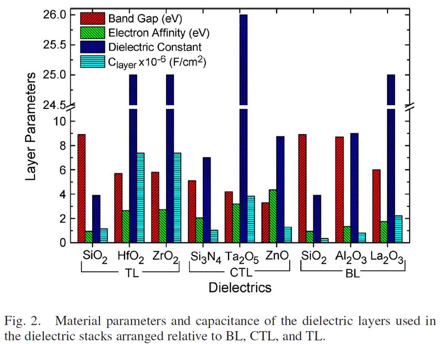
7 Compare and Contrast following Memory Gate Stacks: Stack #: Metal BL CTL TL -S/C Stack 1: TiN O2 3 N4 O 2 p Stack 2: TiN Al 2 O 3 Ta 2 O 5 HfO 2 p Stack 3: TiN La 2 O 3 ZnO ZrO 2 p
8
9

 Appendix 5 From Principles")
10 19 MOSFETs Bandgap Engineering of Channel Consider: Bandgap, mobility, effective mass,lattice matching, quantum confinement of carriers Lattice Constants: a = Å a Ge = Å Cullity, Elements of X-ray Diffraction, 2 nd Ed (1978) Appendix 5 From Principles of Electronic Materials and Devices, Third Edition, S.O. Kasap ( McGraw-Hill, 2005) 20 10


 Appendix 5 IBM RJ Antoniadis et al.")
11 MOSFETs Bandgap Engineering of Channel Consider: Bandgap, mobility, effective mass, lattice matching, quantum confinement of carriers Lattice Constants: a = Å a Ge = Å Cullity, Elements of X-ray Diffraction, 2 nd Ed (1978) Appendix 5 IBM RJ Antoniadis et al., Continuous MOFET Performance Inc with Scaling - Strain & Channel Matl (2006) 21 11
High Dielectric Constant (k) Materials
 Materials") Part 6: High Dielectric Constant (k), Gate Electrode, & Channel Materials O 2 gate ide is approaching physical limits Thickness & Current M O S poly-crystalline V Source W Source Contact Insulator n +
Part 6: High Dielectric Constant (k), Gate Electrode, & Channel Materials O 2 gate ide is approaching physical limits Thickness & Current M O S poly-crystalline V Source W Source Contact Insulator n +
Part 5: Quantum Effects in MOS Devices
 Quantum Effects Lead to Phenomena such as: Ultra Thin Oxides Observe: High Leakage Currents Through the Oxide - Tunneling Depletion in Poly-Si metal gate capacitance effect Thickness of Inversion Layer
Part 4: Heterojunctions - MOS Devices. MOSFET Current Voltage Characteristics
 MOS Device Uses: Part 4: Heterojunctions - MOS Devices MOSCAP capacitor: storing charge, charge-coupled device (CCD), etc. MOSFET transistor: switch, current amplifier, dynamic random access memory (DRAM-volatile),
MSE 310/ECE 340: Electrical Properties of Materials Fall 2014 Department of Materials Science and Engineering Boise State University
 MSE 310/ECE 340: Electrical Properties of Materials Fall 2014 Department of Materials Science and Engineering Boise State University Practice Final Exam 1 Read the questions carefully Label all figures
Quantum Mechanical Simulation for Ultra-thin High-k Gate Dielectrics Metal Oxide Semiconductor Field Effect Transistors
 Mechanical Simulation for Ultra-thin High-k Gate Dielectrics Metal Oxide Semiconductor Field Effect Transistors Shih-Ching Lo 1, Yiming Li 2,3, and Jyun-Hwei Tsai 1 1 National Center for High-Performance
Stretching the Barriers An analysis of MOSFET Scaling. Presenters (in order) Zeinab Mousavi Stephanie Teich-McGoldrick Aseem Jain Jaspreet Wadhwa
 Zeinab Mousavi Stephanie Teich-McGoldrick Aseem Jain Jaspreet Wadhwa") Stretching the Barriers An analysis of MOSFET Scaling Presenters (in order) Zeinab Mousavi Stephanie Teich-McGoldrick Aseem Jain Jaspreet Wadhwa Why Small? Higher Current Lower Gate Capacitance Higher
Stretching the Barriers An analysis of MOSFET Scaling Presenters (in order) Zeinab Mousavi Stephanie Teich-McGoldrick Aseem Jain Jaspreet Wadhwa Why Small? Higher Current Lower Gate Capacitance Higher
Challenges and Opportunities. Prof. J. Raynien Kwo 年
 Nanoelectronics Beyond Si: Challenges and Opportunities Prof. J. Raynien Kwo 年 立 Si CMOS Device Scaling Beyond 22 nm node High κ,, Metal gates, and High mobility channel 1947 First Transistor 1960 1960
A final review session will be offered on Thursday, May 10 from 10AM to 12noon in 521 Cory (the Hogan Room).
.") A final review session will be offered on Thursday, May 10 from 10AM to 12noon in 521 Cory (the Hogan Room). The Final Exam will take place from 12:30PM to 3:30PM on Saturday May 12 in 60 Evans.» All of
A final review session will be offered on Thursday, May 10 from 10AM to 12noon in 521 Cory (the Hogan Room). The Final Exam will take place from 12:30PM to 3:30PM on Saturday May 12 in 60 Evans.» All of
EECS130 Integrated Circuit Devices
 EECS130 Integrated Circuit Devices Professor Ali Javey 10/30/2007 MOSFETs Lecture 4 Reading: Chapter 17, 19 Announcements The next HW set is due on Thursday. Midterm 2 is next week!!!! Threshold and Subthreshold
Gate Carrier Injection and NC-Non- Volatile Memories
 Gate Carrier Injection and NC-Non- Volatile Memories Jean-Pierre Leburton Department of Electrical and Computer Engineering and Beckman Institute University of Illinois at Urbana-Champaign Urbana, IL 61801,
MENA9510 characterization course: Capacitance-voltage (CV) measurements
 measurements") MENA9510 characterization course: Capacitance-voltage (CV) measurements 30.10.2017 Halvard Haug Outline Overview of interesting sample structures Ohmic and schottky contacts Why C-V for solar cells? The
MENA9510 characterization course: Capacitance-voltage (CV) measurements 30.10.2017 Halvard Haug Outline Overview of interesting sample structures Ohmic and schottky contacts Why C-V for solar cells? The
Multiple Gate CMOS and Beyond
 Multiple CMOS and Beyond Dept. of EECS, KAIST Yang-Kyu Choi Outline 1. Ultimate Scaling of MOSFETs - 3nm Nanowire FET - 8nm Non-Volatile Memory Device 2. Multiple Functions of MOSFETs 3. Summary 2 CMOS
Courtesy of S. Salahuddin (UC Berkeley) Lecture 4
 Lecture 4") Courtesy of S. Salahuddin (UC Berkeley) Lecture 4 MOSFET Transport Issues semiconductor band structure quantum confinement effects low-field mobility and high-field saturation Reading: - M. Lundstrom,
Courtesy of S. Salahuddin (UC Berkeley) Lecture 4 MOSFET Transport Issues semiconductor band structure quantum confinement effects low-field mobility and high-field saturation Reading: - M. Lundstrom,
Control of Flat Band Voltage by Partial Incorporation of La 2 O 3 or Sc 2 O 3 into HfO 2 in Metal/HfO 2 /SiO 2 /Si MOS Capacitors
 Control of Flat Band Voltage by Partial Incorporation of La 2 O 3 or Sc 2 O 3 into HfO 2 in Metal/HfO 2 /SiO 2 /Si MOS Capacitors M. Adachi 1, K. Okamoto 1, K. Kakushima 2, P. Ahmet 1, K. Tsutsui 2, N.
Scaling Issues in Planar FET: Dual Gate FET and FinFETs
 Scaling Issues in Planar FET: Dual Gate FET and FinFETs Lecture 12 Dr. Amr Bayoumi Fall 2014 Advanced Devices (EC760) Arab Academy for Science and Technology - Cairo 1 Outline Scaling Issues for Planar
This article has been accepted and published on J-STAGE in advance of copyediting. Content is final as presented.
 This article has been accepted and published on J-STAGE in advance of copyediting. Content is final as presented. References IEICE Electronics Express, Vol.* No.*,*-* Effects of Gamma-ray radiation on
Optimization of the Dielectric Constant of a Blocking Dielectric in the Nonvolatile Memory Based on Silicon Nitride
 ISSN 8756-699, Optoelectronics, Instrumentation and Data Processing, 9, Vol. 45, No. 4, pp. 48 5. c Allerton Press, Inc., 9. Original Russian Text c Y. N. Novikov, V. A. Gritsenko, K. A. Nasyrov, 9, published
Journal of Electron Devices, Vol. 18, 2013, pp JED [ISSN: ]
![Journal of Electron Devices, Vol. 18, 2013, pp JED [ISSN: ]](/thumbs/86/93990983.jpg "Journal of Electron Devices, Vol. 18, 2013, pp JED [ISSN: ]") DrainCurrent-Id in linearscale(a/um) Id in logscale Journal of Electron Devices, Vol. 18, 2013, pp. 1582-1586 JED [ISSN: 1682-3427 ] SUITABILITY OF HIGH-k GATE DIELECTRICS ON THE DEVICE PERFORMANCE AND
DrainCurrent-Id in linearscale(a/um) Id in logscale Journal of Electron Devices, Vol. 18, 2013, pp. 1582-1586 JED [ISSN: 1682-3427 ] SUITABILITY OF HIGH-k GATE DIELECTRICS ON THE DEVICE PERFORMANCE AND
Threshold voltage shift of heteronanocrystal floating gate flash memory
 JOURNAL OF APPLIED PHYSICS 97, 034309 2005 Threshold voltage shift of heteronanocrystal floating gate flash memory Yan Zhu, Dengtao Zhao, Ruigang Li, and Jianlin Liu a Quantum Structures Laboratory, Department
ENERGY BAND diagrams have long been employed to
 236 IEEE TRANSACTIONS ON DEVICE AND MATERIALS RELIABILITY, VOL. 11, NO. 2, JUNE 2011 An Interactive Simulation Tool for Complex Multilayer Dielectric Devices Richard G. Southwick, III, Member, IEEE, Aaron
Electrical and Reliability Characteristics of RRAM for Cross-point Memory Applications. Hyunsang Hwang
 Electrical and Reliability Characteristics of RRAM for Cross-point Memory Applications Hyunsang Hwang Dept. of Materials Science and Engineering Gwangju Institute of Science and Technology (GIST), KOREA
Application of High-κ Gate Dielectrics and Metal Gate Electrodes to enable Silicon and Non-Silicon Logic Nanotechnology
 Application of High-κ Gate Dielectrics and Metal Gate Electrodes to enable Silicon and Non-Silicon Logic Nanotechnology Robert Chau, Justin Brask, Suman Datta, Gilbert Dewey, Mark Doczy, Brian Doyle, Jack
CS 152 Computer Architecture and Engineering
 CS 152 Computer Architecture and Engineering Lecture 12 VLSI II 2005-2-24 John Lazzaro (www.cs.berkeley.edu/~lazzaro) TAs: Ted Hong and David Marquardt www-inst.eecs.berkeley.edu/~cs152/ Last Time: Device
Enhanced Mobility CMOS
 Enhanced Mobility CMOS Judy L. Hoyt I. Åberg, C. Ni Chléirigh, O. Olubuyide, J. Jung, S. Yu, E.A. Fitzgerald, and D.A. Antoniadis Microsystems Technology Laboratory MIT, Cambridge, MA 02139 Acknowledge
EE130: Integrated Circuit Devices
 EE130: Integrated Circuit Devices (online at http://webcast.berkeley.edu) Instructor: Prof. Tsu-Jae King (tking@eecs.berkeley.edu) TA s: Marie Eyoum (meyoum@eecs.berkeley.edu) Alvaro Padilla (apadilla@eecs.berkeley.edu)
(a) (b) Supplementary Figure 1. (a) (b) (a) Supplementary Figure 2. (a) (b) (c) (d) (e)
 (b) Supplementary Figure 1. (a) (b) (a) Supplementary Figure 2. (a) (b) (c) (d) (e)") (a) (b) Supplementary Figure 1. (a) An AFM image of the device after the formation of the contact electrodes and the top gate dielectric Al 2 O 3. (b) A line scan performed along the white dashed line
(a) (b) Supplementary Figure 1. (a) An AFM image of the device after the formation of the contact electrodes and the top gate dielectric Al 2 O 3. (b) A line scan performed along the white dashed line
Defects in Semiconductors
 Defects in Semiconductors Mater. Res. Soc. Symp. Proc. Vol. 1370 2011 Materials Research Society DOI: 10.1557/opl.2011. 771 Electronic Structure of O-vacancy in High-k Dielectrics and Oxide Semiconductors
VSP A gate stack analyzer
 Microelectronics Reliability 47 (7) 74 78 www.elsevier.com/locate/microrel VSP A gate stack analyzer M. Karner *, A. Gehring, M. Wagner, R. Entner, S. Holzer, W. Goes, M. Vasicek, T. Grasser, H. Kosina,
Electrical measurements of voltage stressed Al 2 O 3 /GaAs MOSFET
 Microelectronics Reliability xxx (2007) xxx xxx www.elsevier.com/locate/microrel Electrical measurements of voltage stressed Al 2 O 3 /GaAs MOSFET Z. Tang a, P.D. Ye b, D. Lee a, C.R. Wie a, * a Department
Characteristics Optimization of Sub-10 nm Double Gate Transistors
 Characteristics Optimization of Sub-10 nm Double Gate Transistors YIMING LI 1,,*, JAM-WEM Lee 1, and HONG-MU CHOU 3 1 Departmenet of Nano Device Technology, National Nano Device Laboratories Microelectronics
Comparative studies of Ge and Si p-channel metal oxide semiconductor field-effect-transistors with HfSiON dielectric and TaN metal gate
 Comparative studies of Ge and Si p-channel metal oxide semiconductor field-effect-transistors with HfSiON dielectric and TaN metal gate Hu Ai-Bin( 胡爱斌 ) and Xu Qiu-Xia( 徐秋霞 ) Institute of Microelectronics,
High Mobility Materials and Novel Device Structures for High Performance Nanoscale MOSFETs
 High Mobility Materials and Novel Device Structures for High Performance Nanoscale MOSFETs Prof. (Dr.) Tejas Krishnamohan Department of Electrical Engineering Stanford University, CA & Intel Corporation
ECE-305: Fall 2017 Metal Oxide Semiconductor Devices
 C-305: Fall 2017 Metal Oxide Semiconductor Devices Pierret, Semiconductor Device Fundamentals (SDF) Chapters 15+16 (pp. 525-530, 563-599) Professor Peter Bermel lectrical and Computer ngineering Purdue
L ECE 4211 UConn F. Jain Scaling Laws for NanoFETs Chapter 10 Logic Gate Scaling
 L13 04202017 ECE 4211 UConn F. Jain Scaling Laws for NanoFETs Chapter 10 Logic Gate Scaling Scaling laws: Generalized scaling (GS) p. 610 Design steps p.613 Nanotransistor issues (page 626) Degradation
Lecture 12: MOS Capacitors, transistors. Context
 Lecture 12: MOS Capacitors, transistors Context In the last lecture, we discussed PN diodes, and the depletion layer into semiconductor surfaces. Small signal models In this lecture, we will apply those
The Future of CMOS. David Pulfrey. CHRONOLOGY of the FET. Lecture Lilienfeld s patent (BG FET) 1965 Commercialization (Fairchild)
 1965 Commercialization (Fairchild)") The Future of CMOS David Pulfrey 1 CHRONOLOGY of the FET 1933 Lilienfeld s patent (BG FET) 1965 Commercialization (Fairchild) 1991 The most abundant object made by mankind (C.T. Sah) 2003 The 10 nm FET
The Future of CMOS David Pulfrey 1 CHRONOLOGY of the FET 1933 Lilienfeld s patent (BG FET) 1965 Commercialization (Fairchild) 1991 The most abundant object made by mankind (C.T. Sah) 2003 The 10 nm FET
1 Name: Student number: DEPARTMENT OF PHYSICS AND PHYSICAL OCEANOGRAPHY MEMORIAL UNIVERSITY OF NEWFOUNDLAND. Fall :00-11:00
 1 Name: DEPARTMENT OF PHYSICS AND PHYSICAL OCEANOGRAPHY MEMORIAL UNIVERSITY OF NEWFOUNDLAND Final Exam Physics 3000 December 11, 2012 Fall 2012 9:00-11:00 INSTRUCTIONS: 1. Answer all seven (7) questions.
Lecture 6: 2D FET Electrostatics
 Lecture 6: 2D FET Electrostatics 2016-02-01 Lecture 6, High Speed Devices 2014 1 Lecture 6: III-V FET DC I - MESFETs Reading Guide: Liu: 323-337 (he mainly focuses on the single heterostructure FET) Jena:
CHAPTER 5 EFFECT OF GATE ELECTRODE WORK FUNCTION VARIATION ON DC AND AC PARAMETERS IN CONVENTIONAL AND JUNCTIONLESS FINFETS
 98 CHAPTER 5 EFFECT OF GATE ELECTRODE WORK FUNCTION VARIATION ON DC AND AC PARAMETERS IN CONVENTIONAL AND JUNCTIONLESS FINFETS In this chapter, the effect of gate electrode work function variation on DC
Analytical Modeling of Threshold Voltage for a. Biaxial Strained-Si-MOSFET
 Contemporary Engineering Sciences, Vol. 4, 2011, no. 6, 249 258 Analytical Modeling of Threshold Voltage for a Biaxial Strained-Si-MOSFET Amit Chaudhry Faculty of University Institute of Engineering and
Nanometer Transistors and Their Models. Jan M. Rabaey
 Nanometer Transistors and Their Models Jan M. Rabaey Chapter Outline Nanometer transistor behavior and models Sub-threshold currents and leakage Variability Device and technology innovations Nanometer
CMPEN 411 VLSI Digital Circuits. Lecture 03: MOS Transistor
 CMPEN 411 VLSI Digital Circuits Lecture 03: MOS Transistor Kyusun Choi [Adapted from Rabaey s Digital Integrated Circuits, Second Edition, 2003 J. Rabaey, A. Chandrakasan, B. Nikolic] CMPEN 411 L03 S.1
! CMOS Process Enhancements. ! Semiconductor Physics. " Band gaps. " Field Effects. ! MOS Physics. " Cut-off. " Depletion.
 ESE 570: Digital Integrated Circuits and VLSI Fundamentals Lec 4: January 3, 018 MOS Transistor Theory, MOS Model Lecture Outline! CMOS Process Enhancements! Semiconductor Physics " Band gaps " Field Effects!
Semiconductor Integrated Process Design (MS 635)
") Semiconductor Integrated Process Design (MS 635) Instructor: Prof. Keon Jae Lee - Office: 응용공학동 #4306, Tel: #3343 - Email: keonlee@kaist.ac.kr Lecture: (Tu, Th), 1:00-2:15 #2425 Office hour: Tues & Thur
Semiconductor Integrated Process Design (MS 635) Instructor: Prof. Keon Jae Lee - Office: 응용공학동 #4306, Tel: #3343 - Email: keonlee@kaist.ac.kr Lecture: (Tu, Th), 1:00-2:15 #2425 Office hour: Tues & Thur
Reliability and Instability of GaN MIS-HEMTs for Power Electronics
 Reliability and Instability of GaN MIS-HEMTs for Power Electronics Jesús A. del Alamo, Alex Guo and Shireen Warnock Microsystems Technology Laboratories Massachusetts Institute of Technology 2016 Fall
EE410 vs. Advanced CMOS Structures
 EE410 vs. Advanced CMOS Structures Prof. Krishna S Department of Electrical Engineering S 1 EE410 CMOS Structure P + poly-si N + poly-si Al/Si alloy LPCVD PSG P + P + N + N + PMOS N-substrate NMOS P-well
Lecture 20: Semiconductor Structures Kittel Ch 17, p , extra material in the class notes
 Lecture 20: Semiconductor Structures Kittel Ch 17, p 494-503, 507-511 + extra material in the class notes MOS Structure Layer Structure metal Oxide insulator Semiconductor Semiconductor Large-gap Semiconductor
How a single defect can affect silicon nano-devices. Ted Thorbeck
 How a single defect can affect silicon nano-devices Ted Thorbeck tedt@nist.gov The Big Idea As MOS-FETs continue to shrink, single atomic scale defects are beginning to affect device performance Gate Source
Classification of Solids
 Classification of Solids Classification by conductivity, which is related to the band structure: (Filled bands are shown dark; D(E) = Density of states) Class Electron Density Density of States D(E) Examples
ALD high-k and higher-k integration on GaAs
 ALD high-k and higher-k integration on GaAs Ozhan Koybasi 1), Min Xu 1), Yiqun Liu 2), Jun-Jieh Wang 2), Roy G. Gordon 2), and Peide D. Ye 1)* 1) School of Electrical and Computer Engineering, Purdue University,
Prospects for Ge MOSFETs
 Prospects for Ge MOSFETs Sematech Workshop December 4, 2005 Dimitri A. Antoniadis Microsystems Technology Laboratories MIT Sematech Workshop 2005 1 Channel Transport - I D I D =WQ i (x 0 )v xo v xo : carrier
Capacitance-Voltage characteristics of nanowire trigate MOSFET considering wave functionpenetration
 Global Journal of researches in engineering Electrical and electronics engineering Volume 12 Issue 2 Version 1.0 February 2012 Type: Double Blind Peer Reviewed International Research Journal Publisher:
Integrated Circuits & Systems
 Federal University of Santa Catarina Center for Technology Computer Science & Electronics Engineering Integrated Circuits & Systems INE 5442 Lecture 10 MOSFET part 1 guntzel@inf.ufsc.br ual-well Trench-Isolated
CONSTANT CURRENT STRESS OF ULTRATHIN GATE DIELECTRICS
 CONSTANT CURRENT STRESS OF ULTRATHIN GATE DIELECTRICS Y. Sun School of Electrical & Electronic Engineering Nayang Technological University Nanyang Avenue, Singapore 639798 e-mail: 14794258@ntu.edu.sg Keywords:
Choice of V t and Gate Doping Type
 Choice of V t and Gate Doping Type To make circuit design easier, it is routine to set V t at a small positive value, e.g., 0.4 V, so that, at V g = 0, the transistor does not have an inversion layer and
Frequency dispersion effect and parameters. extraction method for novel HfO 2 as gate dielectric
 048 SCIENCE CHINA Information Sciences April 2010 Vol. 53 No. 4: 878 884 doi: 10.1007/s11432-010-0079-8 Frequency dispersion effect and parameters extraction method for novel HfO 2 as gate dielectric LIU
Solid State Device Fundamentals
 Solid State Device Fundamentals ENS 345 Lecture Course by Alexander M. Zaitsev alexander.zaitsev@csi.cuny.edu Tel: 718 982 2812 Office 4N101b 1 Outline - Goals of the course. What is electronic device?
Low Frequency Noise in MoS 2 Negative Capacitance Field-effect Transistor
 Low Frequency Noise in MoS Negative Capacitance Field-effect Transistor Sami Alghamdi, Mengwei Si, Lingming Yang, and Peide D. Ye* School of Electrical and Computer Engineering Purdue University West Lafayette,
MOS CAPACITOR AND MOSFET
 EE336 Semiconductor Devices 1 MOS CAPACITOR AND MOSFET Dr. Mohammed M. Farag Ideal MOS Capacitor Semiconductor Devices Physics and Technology Chapter 5 EE336 Semiconductor Devices 2 MOS Capacitor Structure
2) Atom manipulation. Xe / Ni(110) Model: Experiment:
 Atom manipulation. Xe / Ni(110) Model: Experiment:") 2) Atom manipulation D. Eigler & E. Schweizer, Nature 344, 524 (1990) Xe / Ni(110) Model: Experiment: G.Meyer, et al. Applied Physics A 68, 125 (1999) First the tip is approached close to the adsorbate
2) Atom manipulation D. Eigler & E. Schweizer, Nature 344, 524 (1990) Xe / Ni(110) Model: Experiment: G.Meyer, et al. Applied Physics A 68, 125 (1999) First the tip is approached close to the adsorbate
New Material Design and Device Simulation Tool. Dr. Gong Kui HZWTECH
 New Material Design and Device Simulation Tool Dr. Gong Kui HZWTECH 鸿之微科技 ( 上海 ) 股份有限公司 HONGZHIWEI TECHNOLOGY(SHANGHAI) CO.,LTD outline Atomistic-TCAD:new devices simulation tool Applications of Atomistic-TCAD
ESE 570: Digital Integrated Circuits and VLSI Fundamentals
 ESE 570: Digital Integrated Circuits and VLSI Fundamentals Lec 4: January 23, 2018 MOS Transistor Theory, MOS Model Penn ESE 570 Spring 2018 Khanna Lecture Outline! CMOS Process Enhancements! Semiconductor
Zuhui Chen, Xing Zhou, Guan Huei See, Zhaomin Zhu, and Guojun Zhu
 Zuhui Chen, Xing Zhou, Guan Huei See, Zhaomin Zhu, and Guojun Zhu School of EEE, Nanyang Technological University, Singapore Slide No.1/18 Outline Motivations. Theory of interface traps. Theory of unified
Improved Interfacial and Electrical Properties of GaSb Metal Oxide
 Improved Interfacial and Electrical Properties of GaSb Metal Oxide Semiconductor Devices Passivated with Acidic (NH 4 ) 2 S Solution Lianfeng Zhao, Zhen Tan, Jing Wang, and Jun Xu * Tsinghua National Laboratory
Operation and Modeling of. The MOS Transistor. Second Edition. Yannis Tsividis Columbia University. New York Oxford OXFORD UNIVERSITY PRESS
 Operation and Modeling of The MOS Transistor Second Edition Yannis Tsividis Columbia University New York Oxford OXFORD UNIVERSITY PRESS CONTENTS Chapter 1 l.l 1.2 1.3 1.4 1.5 1.6 1.7 Chapter 2 2.1 2.2
Electrostatics of Nanowire Transistors
 Electrostatics of Nanowire Transistors Jing Guo, Jing Wang, Eric Polizzi, Supriyo Datta and Mark Lundstrom School of Electrical and Computer Engineering Purdue University, West Lafayette, IN, 47907 ABSTRACTS
Fabrication Technology, Part I
 EEL5225: Principles of MEMS Transducers (Fall 2004) Fabrication Technology, Part I Agenda: Microfabrication Overview Basic semiconductor devices Materials Key processes Oxidation Thin-film Deposition Reading:
ECE 305 Exam 5 SOLUTIONS: Spring 2015 April 17, 2015 Mark Lundstrom Purdue University
 NAME: PUID: : ECE 305 Exam 5 SOLUTIONS: April 17, 2015 Mark Lundstrom Purdue University This is a closed book exam. You may use a calculator and the formula sheet at the end of this exam. Following the
Appendix 1: List of symbols
 Appendix 1: List of symbols Symbol Description MKS Units a Acceleration m/s 2 a 0 Bohr radius m A Area m 2 A* Richardson constant m/s A C Collector area m 2 A E Emitter area m 2 b Bimolecular recombination
R&D Issues for High-k Gate Dielectrics
 R&D Issues for High-k Gate Dielectrics T.P. Ma Yale University Spacer High-k Gate Dielectric Stack Source Drain Gate electrode, poly Upper interfacial region Bulk high-k film Lower interfacial region Substrate
MOS Capacitor MOSFET Devices. MOSFET s. INEL Solid State Electronics. Manuel Toledo Quiñones. ECE Dept. UPRM.
 INEL 6055 - Solid State Electronics ECE Dept. UPRM 20th March 2006 Definitions MOS Capacitor Isolated Metal, SiO 2, Si Threshold Voltage qφ m metal d vacuum level SiO qχ 2 E g /2 qφ F E C E i E F E v qφ
!""#$%&'("')*+,%*-'$(,".,#-#,%'+,/' /.&$0#%#'/(1+,%&'.,',+,(&$+2#'3*24'5.' 6758!9&!
*+,%*-'$(,.,#-#,%'+,/' /.&$0#%#'/(1+,%&'.,',+,(&$+2#'3*24'5.' 6758!9&!") Università di Pisa!""#$%&'("')*+,%*-'$(,".,#-#,%'+,/' /.&$#%#'/(1+,%&'.,',+,(&$+#'3*'5.' 758!9&!!"#$%&'#()"*+"( H%8*'/%I-+/&#J%#)+-+-'%*#J-55K)+&'I*L%&+-M#5-//'&+%,*(#)+&'I*/%,*(#N-5-,&I=+%,*L%&+%(# @+%O-'.%/P#J%#F%.*#!"&,-..-(/#$$#''*$-(
Università di Pisa!""#$%&'("')*+,%*-'$(,".,#-#,%'+,/' /.&$#%#'/(1+,%&'.,',+,(&$+#'3*'5.' 758!9&!!"#$%&'#()"*+"( H%8*'/%I-+/&#J%#)+-+-'%*#J-55K)+&'I*L%&+-M#5-//'&+%,*(#)+&'I*/%,*(#N-5-,&I=+%,*L%&+%(# @+%O-'.%/P#J%#F%.*#!"&,-..-(/#$$#''*$-(
Modern Theory of Solids
 Quantum Mechanical Approach to the Energy Bandgap Knowlton 1 Quantum Mechanical Approach to the Energy Bandgap a+ b = a o = d-spacing of 1D lattice (or plane in 3D) Knowlton 2 Symmetric vs- Asymmetric
A Multi-Gate CMOS Compact Model BSIMMG
 A Multi-Gate CMOS Compact Model BSIMMG Darsen Lu, Sriramkumar Venugopalan, Tanvir Morshed, Yogesh Singh Chauhan, Chung-Hsun Lin, Mohan Dunga, Ali Niknejad and Chenming Hu University of California, Berkeley
STATISTICAL MODELLING OF f t TO PROCESS PARAMETERS IN 30 NM GATE LENGTH FINFETS B. Lakshmi and R. Srinivasan
 STATISTICAL MODELLING OF f t TO PROCESS PARAMETERS IN 30 NM GATE LENGTH FINFETS B. Lakshmi and R. Srinivasan Department of Information Technology SSN College of Engineering, Kalavakkam 603 110, Chennai,
Device 3D. 3D Device Simulator. Nano Scale Devices. Fin FET
 Device 3D 3D Device Simulator Device 3D is a physics based 3D device simulator for any device type and includes material properties for the commonly used semiconductor materials in use today. The physical
ESE370: Circuit-Level Modeling, Design, and Optimization for Digital Systems
 ESE370: Circuit-Level Modeling, Design, and Optimization for Digital Systems Lec 6: September 14, 2015 MOS Model You are Here: Transistor Edition! Previously: simple models (0 and 1 st order) " Comfortable
LECTURE 3 MOSFETS II. MOS SCALING What is Scaling?
 LECTURE 3 MOSFETS II Lecture 3 Goals* * Understand constant field and constant voltage scaling and their effects. Understand small geometry effects for MOS transistors and their implications modeling and
Crystal Properties. MS415 Lec. 2. High performance, high current. ZnO. GaN
 Crystal Properties Crystal Lattices: Periodic arrangement of atoms Repeated unit cells (solid-state) Stuffing atoms into unit cells Determine mechanical & electrical properties High performance, high current
Lecture 18 Field-Effect Transistors 3
 Lecture 18 Field-Effect Transistors 3 Schroder: Chapters, 4, 6 1/38 Announcements Homework 4/6: Is online now. Due Today. I will return it next Wednesday (30 th May). Homework 5/6: It will be online later
Lecture 9. Strained-Si Technology I: Device Physics
 Strain Analysis in Daily Life Lecture 9 Strained-Si Technology I: Device Physics Background Planar MOSFETs FinFETs Reading: Y. Sun, S. Thompson, T. Nishida, Strain Effects in Semiconductors, Springer,
ECE Semiconductor Device and Material Characterization
 EE 483 emiconductor Device and Material haracterization Dr. Alan Doolittle chool of Electrical and omputer Engineering Georgia Institute of Technology As with all of these lecture slides, I am indebted
Quantum-size effects in sub-10 nm fin width InGaAs finfets
 Quantum-size effects in sub-10 nm fin width InGaAs finfets Alon Vardi, Xin Zhao, and Jesús A. del Alamo Microsystems Technology Laboratories, MIT December 9, 2015 Sponsors: DTRA NSF (E3S STC) Northrop
Is IDDQ Testing not Applicable for Deep Submicron VLSI in Year 2011?
 Is IDDQ Testing not Applicable for Deep Submicron VLSI in Year 2011? Chih-Wen Lu Department of Electrical Engineering, Da Yeh University c w lu @ aries. d yu.edu. t w Chung Len Lee Department of Electronics
Analytical Model of Tunneling Current by High Dielectrics and Study of High-k Gate Stack Structure
 Analytical Model of Tunneling Current by High Dielectrics and Study of High-k Gate Stack Structure Swati Mehla 1, Swati Bhasin 2 1 (ECE Department; Geeta Institute of Management and Technology; India)
SEMICONDUCTOR MEMORIES
 SEMICONDUCTOR MEMORIES Semiconductor Memory Classification RWM NVRWM ROM Random Access Non-Random Access EPROM E 2 PROM Mask-Programmed Programmable (PROM) SRAM FIFO FLASH DRAM LIFO Shift Register CAM
Lecture 22 Field-Effect Devices: The MOS Capacitor
 Lecture 22 Field-Effect Devices: The MOS Capacitor F. Cerrina Electrical and Computer Engineering University of Wisconsin Madison Click here for link to F.C. homepage Spring 1999 0 Madison, 1999-II Topics
MOSFET: Introduction
 E&CE 437 Integrated VLSI Systems MOS Transistor 1 of 30 MOSFET: Introduction Metal oxide semiconductor field effect transistor (MOSFET) or MOS is widely used for implementing digital designs Its major
Fundamentals of the Metal Oxide Semiconductor Field-Effect Transistor
 Triode Working FET Fundamentals of the Metal Oxide Semiconductor Field-Effect Transistor The characteristics of energy bands as a function of applied voltage. Surface inversion. The expression for the
Nanoelectronics. Topics
 Nanoelectronics Topics Moore s Law Inorganic nanoelectronic devices Resonant tunneling Quantum dots Single electron transistors Motivation for molecular electronics The review article Overview of Nanoelectronic
Universal Mobility-Field Curves For Electrons In Polysilicon Inversion Layer
 International Journal of Engineering & Computer Science IJECS-IJENS Vol:13 No:5 36 Universal Mobility-Field Curves For Electrons In Polysilicon Inversion Layer M. I. Idris 1, Faiz Arith 2, S. A. M. Chachuli
MOS Capacitors ECE 2204
 MOS apacitors EE 2204 Some lasses of Field Effect Transistors Metal-Oxide-Semiconductor Field Effect Transistor MOSFET, which will be the type that we will study in this course. Metal-Semiconductor Field
SEU RADIATION EFFECTS ON GAA-CNTFET BASED DIGITAL LOGIC CIRCUIT
 International Journal of Mechanical Engineering and Technology (IJMET) Volume 9, Issue 7, July 2018, pp. 345 353, Article ID: IJMET_09_07_039 Available online at http://www.iaeme.com/ijmet/issues.asp?jtype=ijmet&vtype=9&itype=7
Ultra-Scaled InAs HEMTs
 Performance Analysis of Ultra-Scaled InAs HEMTs Neerav Kharche 1, Gerhard Klimeck 1, Dae-Hyun Kim 2,3, Jesús. A. del Alamo 2, and Mathieu Luisier 1 1 Network for Computational ti Nanotechnology and Birck
! CMOS Process Enhancements. ! Semiconductor Physics. " Band gaps. " Field Effects. ! MOS Physics. " Cut-off. " Depletion.
 ESE 570: Digital Integrated Circuits and VLSI Fundamentals Lec 4: January 9, 019 MOS Transistor Theory, MOS Model Lecture Outline CMOS Process Enhancements Semiconductor Physics Band gaps Field Effects
Semiconductor Memories
 Semiconductor References: Adapted from: Digital Integrated Circuits: A Design Perspective, J. Rabaey UCB Principles of CMOS VLSI Design: A Systems Perspective, 2nd Ed., N. H. E. Weste and K. Eshraghian
IBM Research Report. Quantum-Based Simulation Analysis of Scaling in Ultra-Thin Body Device Structures
 RC23248 (W0406-088) June 16, 2004 Electrical Engineering IBM Research Report Quantum-Based Simulation Analysis of Scaling in Ultra-Thin Body Device Structures Arvind Kumar, Jakub Kedzierski, Steven E.
I-V characteristics model for Carbon Nanotube Field Effect Transistors
 International Journal of Engineering & Technology IJET-IJENS Vol:14 No:04 33 I-V characteristics model for Carbon Nanotube Field Effect Transistors Rebiha Marki, Chérifa Azizi and Mourad Zaabat. Abstract--
Solid-State Electronics
 Solid-State Electronics 52 (2008) 1884 1888 Contents lists available at ScienceDirect Solid-State Electronics journal homepage: www.elsevier.com/locate/sse Analysis of STI-induced mechanical stress-related
Ion Implantation. alternative to diffusion for the introduction of dopants essentially a physical process, rather than chemical advantages:
 Ion Implantation alternative to diffusion for the introduction of dopants essentially a physical process, rather than chemical advantages: mass separation allows wide varies of dopants dose control: diffusion