Minimizing Clock Latency Range in Robust Clock Tree Synthesis
|
|
|
- Hilary Casey
- 5 years ago
- Views:
Transcription
1 Minimizing Clock Latency Range in Robust Clock Tree Synthesis Wen-Hao Liu Yih-Lang Li Hui-Chi Chen You have to enlarge your font. Many pages are hard to view. I think the position of Page topic is too low such that the content space is limited. Replace this format by Lab slide format. Add page number.
2 2 Outline Introduction Problem Formulation Algorithm Overview Obstacle-Avoiding Balanced Clock Tree Routing Monotonic Parallel BIWS Experimental Results Conclusions
3 3 Introduction Clock network synthesis has played an important role in determining circuit performance. Skew is still one of the most important indicators. clock peri od td + tskew + tsu + t ds t d : Longest path through combinational logic t skew : Clock skew t su : Setup time of the synchronizing elements t ds : Propagation delay within the synchronizing element
4 4 Introduction The signal degrades when propagating through a long routing wire (slew problem). Therefore, we need to insert buffers to repower the signal line so as to maintain adequate slew rate. Pre-placed IPs and macro blocks in a design are thought as obstacles which obstruct buffer insertion.
5 Introduction Variation of clock tree has to be concerned (Voltage variation, process variation, noise etc). In the ISPD 09 Clock Network Synthesis (CNS) contest, the primary goal is to minimize the clock latency range (CLR) across different supply-voltage simulations under given slew rate, obstacle, total capacitance constraints. To the best of our knowledge, no work has yet addressed CLR minimization.
6 6 Outline Introduction Problem Formulation Algorithm Overview Obstacle-Avoiding Balanced Clock Tree Routing Monotonic Parallel BIWS Experimental Results Conclusions
7 7 Problem Formulation Clock Network Synthesis (CNS): Given: a 8-tuple (S, SNK, OB, Ψ, W, V, Cap limit, Slew limit ) Objective: the CNS problem is to construct a clock tree such that CLR(BT S ) is minimal. Subject to: tcap(bt S ) Cap limit, slew(b_s) Slew limit, b_s BF(BT S ) SNK; Buffers are not allowed to overlap obstacles. S: source SNK: a set of sinks with sink locations OB: a set of obstacles Ψ :a buffer library W:a wire library V:a set of multiple supply voltages Cap limit : total capacitance constraint Slew limit : slew constraint
8 8 Problem Formulation Clock latency Range (CLR) The maximum difference of each sink s latency across different voltages CLR(BT S ) <=skew(bt S ) + MDV(BT S ) MDV(BT v ) is maximum source-to-sink delay variation across multiple supply voltages. BT s 1 s 2 1V V 10 8 CLR(BT S ) =15-8=7 skew(bt S ) =max(15-12, 10-8)=3 MDV(BT S ) =max(15-10, 12-8)=5
9 9 Outline Introduction Problem Formulation Algorithm Overview Obstacle-Avoiding Balanced Clock Tree Routing Monotonic Parallel BIWS Experimental Results Conclusions


10 Algorithm Flow An un-buffered tree T s An buffered tree BT s


11 Algorithm Flow The goal at the first stage is to identify a balanced un-buffered zero-skew clock tree TS with minimal wirelength. In the second stage, monotonic parallel BIWS algorithm inserts parallel buffers and performs wire sizing to minimize??? under capacitance and slew constraints. The third stage invokes ngspice to calculate accurately the delay of each sink, and then inserts snaking wires along the path of the small delay to reduce skew. Input After stage1 After stage2&3
12 12 Outline Introduction Problem Formulation Algorithm Overview Obstacle-Avoiding Balanced Clock Tree Routing Obstacle-Aware Balanced Clock-Tree Generation Obstacle- Avoiding Rectilinear Routing Monotonic Parallel BIWS Experimental Results Conclusions
13 Obstacle-Aware Balanced Clock-Tree Generation This approach provides tree topology and internal node location. the clustering-based method is adapted. Given n sinks, every sink is initially regarded as an individual zero-skew sub-tree. The operation merges two sub-trees as a new zero-skew sub-tree.
14 Obstacle-Aware Balanced Clock-Tree Generation In this work, three factors determine the candidates for merging. Wirelength of connecting two sub-tree (this item is the same as the next item, do u mean wirelength of connected two sub-trees. It means the total wirelength of the new tree that connects two sub-trees) Wirelength of the new wires that are required for tree merging, inside the obstacles 2 To generate τ ( t1, t2 ) = balanced α * wire( t1, tree, t2 ) + we β * ubw choose ( t1, t2 two ) sub-trees with low capacitance + γ * ( tcap for ( t merging. ) + tcap( t )) 1 2
15 Obstacle- Avoiding Rectilinear Routing 1) Construct a non-uniform grid routing graph by extending all borders of all obstacles. 2) Monotonic routing is adopted to seek the rectilinear routing of every tree edge. 3) If the length of a tree edge inside an obstacle exceeds L, then the maze routing is invoked to reroute this tree edge to reduce the wirelength inside an obstacle. n 1 n 1 n 1 n 1 s 1 s 1 s 1 s 1
16 Outline Introduction Problem Formulation Algorithm Overview Obstacle-Avoiding Balanced Clock Tree Routing Monotonic Parallel BIWS CLR-driven BIWS Re-Buffered Tree Extraction using Amplified Capacitance Experimental Results Conclusions 16
17 Monotonic Parallel BIWS What is parallel buffer? Why use parallel buffer? Type Parallel buffer Cap intrinsic delay at 1V intrinsic delay at 1.2V Delay variation (DV) among 1V and 1.2V
18 Monotonic Parallel BIWS CLR(BT S ) skew(bt S ) + MDV(BT S ) To the best of our knowledge, the MDV minimization has not been investigated. In monotonic parallel BIWS, parallel buffers are exploited to decline MDV. Traditional BIWS algorithms [4][5][6][8] have to search a large solution space if the buffer library becomes large.


19 The font is too small. Try to reduce the word count. The position of The topic is too low such that the content space is reduced. Monotonic Parallel BIWS The proposed buffer insertion strategy is to place the least-dv parallel buffer as close as possible to the source, to reduce MDV of every path from source to every sink. In this work the solution space does not increase markedly because of using single type of parallel buffers in each re-buffering iteration.
20 The font is too small. Try to reduce the word count. The position of The topic is too low such that the content space is reduced. CLR-Driven BIWS Given an un-buffered tree, CLR-driven BIWS seeks out a minimum weighted-clr buffered clock tree. The weighted-clr is defined as follows: WCLR (BTS) = skew(bts)+ω MDV(BTS), ω>1 CLR-driven BIWS is a Ginneken-like algorithm that enumerates all possible BIWS solutions and then selects the minimum weighted-clr solution from all solutions. Pruning redundant solutions is a principal issue in designing an efficient Ginneken-like algorithm. Look-ahead violation-detecting scheme Grouping and pruning suboptimal solutions Pruning surplus solutions
21 Re-Buffered Tree Extraction using Amplified Capacitance
22 22 Outline Introduction Problem Formulation Algorithm Overview Obstacle-Avoiding Balanced Clock Tree Routing Monotonic Parallel BIWS Experimental Results Conclusions
23 Experimental Environment ISPD09 benchmarks were used. Machine: Intel Xeon 3.0GHz CPU and 16GB RAM. Runtime is normalized according to the clock rate ratio. The template of this page is different from the other.
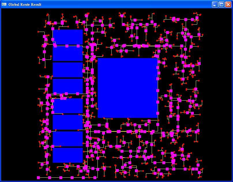
24 Routing Result Statistics
25 Routing Result Statistics


26 Routing Result Statistics
27 ISPD 09 Clock Network Synthesis Contest CLR CAP CPU 0 ours (7) A. National Taiwan Univ (6) B. Univ of Michigan (7) C. Purdue & National Tsing Hua Univ (7) D. National Chiao Tung Univ (5) E. Chinese Univ of Hong Kong (3) F. Polytechnic Univ of Hong Kong (5) G.National Cheng Kung Univ (5)

28 Synthesis result
29 29 Outline Introduction Problem Formulation Algorithm Overview Obstacle-Avoiding Balanced Clock Tree Routing Monotonic Parallel BIWS Experimental Results Conclusions
30 Conclusions In this work, a three-stage CLR-driven CTS flow is proposed. An obstacle-avoiding balanced clock tree routing algorithm identifies a balanced clock tree with minimal wirelength to minimize clock skew and wire capacitance. An efficient monotonic parallel BIWS algorithm is presented to a minimum-weighted-clr buffered clock tree. The proposed CLR-driven CTS flow can complete all ISPD 09 benchmark circuits and yield 59%, 52.7% and 35.4% lower CLRs than those produced by the top three performers of the ISPD 09 CNS contest.
ISPD 2009 Clock Network Synthesis Contest
 ISPD 00 Clock Network Synthesis Contest Cliff Sze and Phillip Restle IBM Research Why this Contest Is So Different from the Previous? Placement and global routing hard problems with simple rules Wirelength,
Making Fast Buffer Insertion Even Faster via Approximation Techniques
 Making Fast Buffer Insertion Even Faster via Approximation Techniques Zhuo Li, C. N. Sze, Jiang Hu and Weiping Shi Department of Electrical Engineering Texas A&M University Charles J. Alpert IBM Austin
CSE241 VLSI Digital Circuits Winter Lecture 07: Timing II
 CSE241 VLSI Digital Circuits Winter 2003 Lecture 07: Timing II CSE241 L3 ASICs.1 Delay Calculation Cell Fall Cap\Tr 0.05 0.2 0.5 0.01 0.02 0.16 0.30 0.5 2.0 0.04 0.32 0.178 0.08 0.64 0.60 1.20 0.1ns 0.147ns
Logic Synthesis and Verification
 Logic Synthesis and Verification Jie-Hong Roland Jiang 江介宏 Department of Electrical Engineering National Taiwan University Fall Timing Analysis & Optimization Reading: Logic Synthesis in a Nutshell Sections
UTPlaceF 3.0: A Parallelization Framework for Modern FPGA Global Placement
 UTPlaceF 3.0: A Parallelization Framework for Modern FPGA Global Placement Wuxi Li, Meng Li, Jiajun Wang, and David Z. Pan University of Texas at Austin wuxili@utexas.edu November 14, 2017 UT DA Wuxi Li
Utilizing Redundancy for Timing Critical Interconnect
 1 Utilizing Redundancy for Timing Critical Interconnect Shiyan Hu, Qiuyang Li, Jiang Hu, Peng Li Abstract Conventionally, the topology of signal net routing is almost always restricted to Steiner trees,
Implementation of Clock Network Based on Clock Mesh
 International Conference on Information Technology and Management Innovation (ICITMI 2015) Implementation of Clock Network Based on Clock Mesh He Xin 1, a *, Huang Xu 2,b and Li Yujing 3,c 1 Sichuan Institute
Buffered Clock Tree Sizing for Skew Minimization under Power and Thermal Budgets
 Buffered Clock Tree Sizing for Skew Minimization under Power and Thermal Budgets Krit Athikulwongse, Xin Zhao, and Sung Kyu Lim School of Electrical and Computer Engineering Georgia Institute of Technology
Variation-aware Clock Network Design Methodology for Ultra-Low Voltage (ULV) Circuits
 Circuits") Variation-aware Clock Network Design Methodology for Ultra-Low Voltage (ULV) Circuits Xin Zhao, Jeremy R. Tolbert, Chang Liu, Saibal Mukhopadhyay, and Sung Kyu Lim School of ECE, Georgia Institute of Technology,
Variation-aware Clock Network Design Methodology for Ultra-Low Voltage (ULV) Circuits Xin Zhao, Jeremy R. Tolbert, Chang Liu, Saibal Mukhopadhyay, and Sung Kyu Lim School of ECE, Georgia Institute of Technology,
Timing-Aware Decoupling Capacitance Allocation in Power Distribution Networks
 Timing-Aware Decoupling Capacitance Allocation in Power Distribution Networks Sanjay Pant, David Blaauw Electrical Engineering and Computer Science University of Michigan 1/22 Power supply integrity issues
Clock Buffer Polarity Assignment Utilizing Useful Clock Skews for Power Noise Reduction
 Clock Buffer Polarity Assignment Utilizing Useful Clock Skews for Power Noise Reduction Deokjin Joo and Taewhan Kim Department of Electrical and Computer Engineering, Seoul National University, Seoul,
392 IEEE TRANSACTIONS ON COMPUTER-AIDED DESIGN OF INTEGRATED CIRCUITS AND SYSTEMS, VOL. 32, NO. 3, MARCH 2013
 392 IEEE TRANSACTIONS ON COMPUTER-AIDED DESIGN OF INTEGRATED CIRCUITS AND SYSTEMS, VOL. 32, NO. 3, MARCH 2013 An Optimal Allocation Algorithm of Adjustable Delay Buffers and Practical Extensions for Clock
Fast Buffer Insertion Considering Process Variation
 Fast Buffer Insertion Considering Process Variation Jinjun Xiong, Lei He EE Department University of California, Los Angeles Sponsors: NSF, UC MICRO, Actel, Mindspeed Agenda Introduction and motivation
An Optimal Algorithm of Adjustable Delay Buffer Insertion for Solving Clock Skew Variation Problem
 An Optimal Algorithm of Adjustable Delay Buffer Insertion for Solving Clock Skew Variation Problem Juyeon Kim 1 juyeon@ssl.snu.ac.kr Deokjin Joo 1 jdj@ssl.snu.ac.kr Taewhan Kim 1,2 tkim@ssl.snu.ac.kr 1
ESE 570: Digital Integrated Circuits and VLSI Fundamentals
 ESE 570: Digital Integrated Circuits and VLSI Fundamentals Lec 24: April 19, 2018 Crosstalk and Wiring, Transmission Lines Lecture Outline! Crosstalk! Repeaters in Wiring! Transmission Lines " Where transmission
! Crosstalk. ! Repeaters in Wiring. ! Transmission Lines. " Where transmission lines arise? " Lossless Transmission Line.
 ESE 570: Digital Integrated Circuits and VLSI Fundamentals Lec 24: April 19, 2018 Crosstalk and Wiring, Transmission Lines Lecture Outline! Crosstalk! Repeaters in Wiring! Transmission Lines " Where transmission
Thermal-reliable 3D Clock-tree Synthesis Considering Nonlinear Electrical-thermal-coupled TSV Model
 Thermal-reliable 3D Clock-tree Synthesis Considering Nonlinear Electrical-thermal-coupled TSV Model Yang Shang 1, Chun Zhang 1, Hao Yu 1, Chuan Seng Tan 1, Xin Zhao 2, Sung Kyu Lim 2 1 School of Electrical
Power-Driven Global Routing for Multi-Supply Voltage Domains
 Power-Driven Global Routing for Multi-Supply Voltage Domains Tai-Hsuan Wu, Azadeh Davoodi, and Jeffrey T. Linderoth Department of Electrical and Computer Engineering Department of Industrial and Systems
Large-Scale Behavioral Targeting
 Large-Scale Behavioral Targeting Ye Chen, Dmitry Pavlov, John Canny ebay, Yandex, UC Berkeley (This work was conducted at Yahoo! Labs.) June 30, 2009 Chen et al. (KDD 09) Large-Scale Behavioral Targeting
Physical Design of Digital Integrated Circuits (EN0291 S40) Sherief Reda Division of Engineering, Brown University Fall 2006
 Sherief Reda Division of Engineering, Brown University Fall 2006") Physical Design of Digital Integrated Circuits (EN0291 S40) Sherief Reda Division of Engineering, Brown University Fall 2006 1 Lecture 04: Timing Analysis Static timing analysis STA for sequential circuits
Physical Design of Digital Integrated Circuits (EN0291 S40) Sherief Reda Division of Engineering, Brown University Fall 2006 1 Lecture 04: Timing Analysis Static timing analysis STA for sequential circuits
ULTRALOW VOLTAGE (ULV) circuits, where the supply
 circuits, where the supply") 1222 IEEE TRANSACTIONS ON COMPUTER-AIDED DESIGN OF INTEGRATED CIRCUITS AND SYSTEMS, VOL. 31, NO. 8, AUGUST 2012 Variation-Aware Clock Network Design Methodology for Ultralow Voltage (ULV) Circuits Xin
1222 IEEE TRANSACTIONS ON COMPUTER-AIDED DESIGN OF INTEGRATED CIRCUITS AND SYSTEMS, VOL. 31, NO. 8, AUGUST 2012 Variation-Aware Clock Network Design Methodology for Ultralow Voltage (ULV) Circuits Xin
Lecture 23. Dealing with Interconnect. Impact of Interconnect Parasitics
 Lecture 23 Dealing with Interconnect Impact of Interconnect Parasitics Reduce Reliability Affect Performance Classes of Parasitics Capacitive Resistive Inductive 1 INTERCONNECT Dealing with Capacitance
TAU 2015 Contest Incremental Timing Analysis and Incremental Common Path Pessimism Removal (CPPR) Contest Education. v1.9 January 19 th, 2015
 Contest Education. v1.9 January 19 th, 2015") TU 2015 Contest Incremental Timing nalysis and Incremental Common Path Pessimism Removal CPPR Contest Education v1.9 January 19 th, 2015 https://sites.google.com/site/taucontest2015 Contents 1 Introduction
TU 2015 Contest Incremental Timing nalysis and Incremental Common Path Pessimism Removal CPPR Contest Education v1.9 January 19 th, 2015 https://sites.google.com/site/taucontest2015 Contents 1 Introduction
The Fast Optimal Voltage Partitioning Algorithm For Peak Power Density Minimization
 The Fast Optimal Voltage Partitioning Algorithm For Peak Power Density Minimization Jia Wang, Shiyan Hu Department of Electrical and Computer Engineering Michigan Technological University Houghton, Michigan
Issues on Timing and Clocking
 ECE152B TC 1 Issues on Timing and Clocking X Combinational Logic Z... clock clock clock period ECE152B TC 2 Latch and Flip-Flop L CK CK 1 L1 1 L2 2 CK CK CK ECE152B TC 3 Clocking X Combinational Logic...
Next, we check the race condition to see if the circuit will work properly. Note that the minimum logic delay is a single sum.
 UNIVERSITY OF CALIFORNIA College of Engineering Department of Electrical Engineering and Computer Sciences Last modified on May 1, 2003 by Dejan Markovic (dejan@eecs.berkeley.edu) Prof. Jan Rabaey EECS
Clock signal in digital circuit is responsible for synchronizing the transfer to the data between processing elements.
 1 2 Introduction Clock signal in digital circuit is responsible for synchronizing the transfer to the data between processing elements. Defines the precise instants when the circuit is allowed to change
A Practical Clock Tree Synthesis for Semi-Synchronous Circuits
 A Practical Clock Tree Synthesis for Semi-Synchronous Circuits Masahiko Toyonaga, Keiichi Kurokawa, Takuya Yasui Corporate Semiconductor Development Division Matsushita Electric Industrial Co., Ltd. 3-1-1,
iretilp : An efficient incremental algorithm for min-period retiming under general delay model
 iretilp : An efficient incremental algorithm for min-period retiming under general delay model Debasish Das, Jia Wang and Hai Zhou EECS, Northwestern University, Evanston, IL 60201 Place and Route Group,
Micro-architecture Pipelining Optimization with Throughput- Aware Floorplanning
 Micro-architecture Pipelining Optimization with Throughput- Aware Floorplanning Yuchun Ma* Zhuoyuan Li* Jason Cong Xianlong Hong Glenn Reinman Sheqin Dong* Qiang Zhou *Department of Computer Science &
Timing Driven Power Gating in High-Level Synthesis
 Timing Driven Power Gating in High-Level Synthesis Shih-Hsu Huang and Chun-Hua Cheng Department of Electronic Engineering Chung Yuan Christian University, Taiwan Outline Introduction Motivation Our Approach
Lecture 9: Clocking, Clock Skew, Clock Jitter, Clock Distribution and some FM
 Lecture 9: Clocking, Clock Skew, Clock Jitter, Clock Distribution and some FM Mark McDermott Electrical and Computer Engineering The University of Texas at Austin 9/27/18 VLSI-1 Class Notes Why Clocking?
TAU 2014 Contest Pessimism Removal of Timing Analysis v1.6 December 11 th,
 TU 2014 Contest Pessimism Removal of Timing nalysis v1.6 ecember 11 th, 2013 https://sites.google.com/site/taucontest2014 1 Introduction This document outlines the concepts and implementation details necessary
A Novel Cell Placement Algorithm for Flexible TFT Circuit with Mechanical Strain and Temperature Consideration
 A Novel Cell Placement Algorithm for Flexible TFT Circuit with Mechanical Strain and Temperature Consideration Jiun-Li Lin, Po-Hsun Wu, and Tsung-Yi Ho Department of Computer Science and Information Engineering,
Luis Manuel Santana Gallego 71 Investigation and simulation of the clock skew in modern integrated circuits. Clock Skew Model 1
 Luis Manuel Santana Gallego 71 Appendix 1 Clock Skew Model 1 Steven D. Kugelmass, Kenneth Steiglitz [KUG-88] 1. Introduction The accumulation of clock skew, the differences in arrival times of signal in
Signal integrity in deep-sub-micron integrated circuits
 Signal integrity in deep-sub-micron integrated circuits Alessandro Bogliolo abogliolo@ing.unife.it Outline Introduction General signaling scheme Noise sources and effects in DSM ICs Supply noise Synchronization
Skew Management of NBTI Impacted Gated Clock Trees
 International Symposium on Physical Design 2010 Skew Management of NBTI Impacted Gated Clock Trees Ashutosh Chakraborty and David Z. Pan ECE Department, University of Texas at Austin ashutosh@cerc.utexas.edu
Lecture 25. Dealing with Interconnect and Timing. Digital Integrated Circuits Interconnect
 Lecture 25 Dealing with Interconnect and Timing Administrivia Projects will be graded by next week Project phase 3 will be announced next Tu.» Will be homework-like» Report will be combined poster Today
Digital Integrated Circuits. The Wire * Fuyuzhuo. *Thanks for Dr.Guoyong.SHI for his slides contributed for the talk. Digital IC.
 Digital Integrated Circuits The Wire * Fuyuzhuo *Thanks for Dr.Guoyong.SHI for his slides contributed for the talk Introduction The Wire transmitters receivers schematics physical 2 Interconnect Impact
Multi-Approximate-Keyword Routing Query
 Bin Yao 1, Mingwang Tang 2, Feifei Li 2 1 Department of Computer Science and Engineering Shanghai Jiao Tong University, P. R. China 2 School of Computing University of Utah, USA Outline 1 Introduction
CMPEN 411 VLSI Digital Circuits Spring 2012 Lecture 17: Dynamic Sequential Circuits And Timing Issues
 CMPEN 411 VLSI Digital Circuits Spring 2012 Lecture 17: Dynamic Sequential Circuits And Timing Issues [Adapted from Rabaey s Digital Integrated Circuits, Second Edition, 2003 J. Rabaey, A. Chandrakasan,
Outline. Week 5: Circuits. Course Notes: 3.5. Goals: Use linear algebra to determine voltage drops and branch currents.
 Outline Week 5: Circuits Course Notes: 3.5 Goals: Use linear algebra to determine voltage drops and branch currents. Components in Resistor Networks voltage source current source resistor Components in
Online Scheduling Switch for Maintaining Data Freshness in Flexible Real-Time Systems
 Online Scheduling Switch for Maintaining Data Freshness in Flexible Real-Time Systems Song Han 1 Deji Chen 2 Ming Xiong 3 Aloysius K. Mok 1 1 The University of Texas at Austin 2 Emerson Process Management
Models for representing sequential circuits
 Sequential Circuits Models for representing sequential circuits Finite-state machines (Moore and Mealy) Representation of memory (states) Changes in state (transitions) Design procedure State diagrams
Timing Analysis with Clock Skew
 , Mark Horowitz 1, & Dean Liu 1 David_Harris@hmc.edu, {horowitz, dliu}@vlsi.stanford.edu March, 1999 Harvey Mudd College Claremont, CA 1 (with Stanford University, Stanford, CA) Outline Introduction Timing
A Random Walk from Async to Sync. Paul Cunningham & Steev Wilcox
 A Random Walk from Async to Sync Paul Cunningham & Steev Wilcox Thank You Ivan In the Beginning March 2002 Azuro Day 1 Some money in the bank from Angel Investors 2 employees Small Office rented from Cambridge
Topics to be Covered. capacitance inductance transmission lines
 Topics to be Covered Circuit Elements Switching Characteristics Power Dissipation Conductor Sizes Charge Sharing Design Margins Yield resistance capacitance inductance transmission lines Resistance of
Smart Non-Default Routing for Clock Power Reduction
 Smart Non-Default Routing for Clock Power Reduction Andrew B. Kahng, Seokhyeong Kang and Hyein Lee ECE and CSE Departments, University of California at San Diego abk@ucsd.edu, shkang@vlsicad.ucsd.edu,
Clock Skew Scheduling in the Presence of Heavily Gated Clock Networks
 Clock Skew Scheduling in the Presence of Heavily Gated Clock Networks ABSTRACT Weicheng Liu, Emre Salman Department of Electrical and Computer Engineering Stony Brook University Stony Brook, NY 11794 [weicheng.liu,
Skew Management of NBTI Impacted Gated Clock Trees
 Skew Management of NBTI Impacted Gated Clock Trees Ashutosh Chakraborty ECE Department The University of Texas at Austin Austin, TX 78703, USA ashutosh@cerc.utexas.edu David Z. Pan ECE Department The University
Luis Manuel Santana Gallego 31 Investigation and simulation of the clock skew in modern integrated circuits
 Luis Manuel Santana Gallego 31 Investigation and simulation of the clock skew in modern egrated circuits 3. Clock skew 3.1. Definitions For two sequentially adjacent registers, as shown in figure.1, C
Solution (a) We can draw Karnaugh maps for NS1, NS0 and OUT:
 We can draw Karnaugh maps for NS1, NS0 and OUT:") DIGITAL ELECTRONICS II Revision Examples 7 Exam Format Q compulsory + any out of Q, Q, Q4. Q has 5 parts worth 8% each, Q,,4 are worth %. Revision Lectures Three revision lectures will be given on the
DIGITAL ELECTRONICS II Revision Examples 7 Exam Format Q compulsory + any out of Q, Q, Q4. Q has 5 parts worth 8% each, Q,,4 are worth %. Revision Lectures Three revision lectures will be given on the
Pipelining and Parallel Processing
 Pipelining and Parallel Processing ( 范倫達 ), Ph. D. Department of Computer Science National Chiao Tung University Taiwan, R.O.C. Fall, 010 ldvan@cs.nctu.edu.tw http://www.cs.nctu.edu.tw/~ldvan/ Outlines
Buffer sizing for Clock Networks Using Robust Geometric Programming
 Buffer sizing for Clock Networks Using Robust Geometric Programming Laleh Behjat, Logan Rakai, Amin Farshidi, Dave Westwick University of Calgary, Calgary, Canada March 27, 2013 The essence of Mathematics
Perfect-Balance Planar Clock. Routing with Minimal Path Length UCSC-CRL March 26, University of California, Santa Cruz
 Perfect-Balance Planar Clock Routing with Minimal Path Length Qing Zhu Wayne W.M. Dai UCSC-CRL-93-17 supercedes UCSC-CRL-92-12 March 26, 1993 Board of Studies in Computer Engineering University of California,
Thermal-reliable 3D Clock-tree Synthesis Considering Nonlinear Electrical-thermal-coupled TSV Model
 Thermal-reliable 3D Clock-tree Synthesis Considering Nonlinear Electrical-thermal-coupled TSV Model Yang Shang, Chun Zhang, Hao Yu, Chuan Seng Tan Xin Zhao, Sung Kyu Lim School of Electrical and Electronic
Lecture 21: Packaging, Power, & Clock
 Lecture 21: Packaging, Power, & Clock Outline Packaging Power Distribution Clock Distribution 2 Packages Package functions Electrical connection of signals and power from chip to board Little delay or
Buffer Insertion for Noise and Delay Optimization
 Buffer Insertion for Noise and Delay Optimization Charles J Alpert IBM Austin esearch Laoratory Austin, TX 78660 alpert@austinimcom Anirudh Devgan IBM Austin esearch Laoratory Austin, TX 78660 devgan@austinimcom
Itanium TM Processor Clock Design
 Itanium TM Processor Design Utpal Desai 1, Simon Tam, Robert Kim, Ji Zhang, Stefan Rusu Intel Corporation, M/S SC12-502, 2200 Mission College Blvd, Santa Clara, CA 95052 ABSTRACT The Itanium processor
Steiner Trees in Chip Design. Jens Vygen. Hangzhou, March 2009
 Steiner Trees in Chip Design Jens Vygen Hangzhou, March 2009 Introduction I A digital chip contains millions of gates. I Each gate produces a signal (0 or 1) once every cycle. I The output signal of a
Lecture 5: DC & Transient Response
 Lecture 5: DC & Transient Response Outline q Pass Transistors q DC Response q Logic Levels and Noise Margins q Transient Response q RC Delay Models q Delay Estimation 2 Activity 1) If the width of a transistor
Chapter 5 CMOS Logic Gate Design
 Chapter 5 CMOS Logic Gate Design Section 5. -To achieve correct operation of integrated logic gates, we need to satisfy 1. Functional specification. Temporal (timing) constraint. (1) In CMOS, incorrect
Lecture 6: DC & Transient Response
 Lecture 6: DC & Transient Response Slides courtesy of Deming Chen Slides based on the initial set from David Harris CMOS VLSI Design Outline Pass Transistors DC Response Logic Levels and Noise Margins
Clock Strategy. VLSI System Design NCKUEE-KJLEE
 Clock Strategy Clocked Systems Latch and Flip-flops System timing Clock skew High speed latch design Phase locked loop ynamic logic Multiple phase Clock distribution Clocked Systems Most VLSI systems are
Adding a New Dimension to Physical Design. Sachin Sapatnekar University of Minnesota
 Adding a New Dimension to Physical Design Sachin Sapatnekar University of Minnesota 1 Outline What is 3D about? Why 3D? 3D-specific challenges 3D analysis and optimization 2 Planning a city: Land usage
Hardware Design I Chap. 4 Representative combinational logic
 Hardware Design I Chap. 4 Representative combinational logic E-mail: shimada@is.naist.jp Already optimized circuits There are many optimized circuits which are well used You can reduce your design workload
Logic BIST. Sungho Kang Yonsei University
 Logic BIST Sungho Kang Yonsei University Outline Introduction Basics Issues Weighted Random Pattern Generation BIST Architectures Deterministic BIST Conclusion 2 Built In Self Test Test/ Normal Input Pattern
Design for Variability and Signoff Tips
 Design for Variability and Signoff Tips Alexander Tetelbaum Abelite Design Automation, Walnut Creek, USA alex@abelite-da.com ABSTRACT The paper provides useful design tips and recommendations on how to
CROSSTALK NOISE ANALYSIS FOR NANO-METER VLSI CIRCUITS
 CROSSTALK NOISE ANALYSIS FOR NANO-METER VLSI CIRCUITS by Ravikishore Gandikota A dissertation submitted in partial fulfillment of the requirements for the degree of Doctor of Philosophy (Electrical Engineering)
Digital Integrated Circuits A Design Perspective. Arithmetic Circuits. Jan M. Rabaey Anantha Chandrakasan Borivoje Nikolic.
 Digital Integrated Circuits A Design Perspective Jan M. Rabaey Anantha Chandrakasan Borivoje Nikolic Arithmetic Circuits January, 2003 1 A Generic Digital Processor MEMORY INPUT-OUTPUT CONTROL DATAPATH
Digital VLSI Design. Lecture 8: Clock Tree Synthesis
 Digital VLSI Design Lecture 8: Clock Tree Synthesis Semester A, 2018-19 Lecturer: Dr. Adam Teman January 12, 2019 Disclaimer: This course was prepared, in its entirety, by Adam Teman. Many materials were
Consensus Algorithms for Camera Sensor Networks. Roberto Tron Vision, Dynamics and Learning Lab Johns Hopkins University
 Consensus Algorithms for Camera Sensor Networks Roberto Tron Vision, Dynamics and Learning Lab Johns Hopkins University Camera Sensor Networks Motes Small, battery powered Embedded camera Wireless interface
Integrated Circuits & Systems
 Federal University of Santa Catarina Center for Technology Computer Science & Electronics Engineering Integrated Circuits & Systems INE 5442 Lecture 18 CMOS Sequential Circuits - 1 guntzel@inf.ufsc.br
Problems in VLSI design
 Problems in VLSI design wire and transistor sizing signal delay in RC circuits transistor and wire sizing Elmore delay minimization via GP dominant time constant minimization via SDP placement problems
Digital Integrated Circuits A Design Perspective. Arithmetic Circuits. Jan M. Rabaey Anantha Chandrakasan Borivoje Nikolic.
 Digital Integrated Circuits A Design Perspective Jan M. Rabaey Anantha Chandrakasan Borivoje Nikolic Arithmetic Circuits January, 2003 1 A Generic Digital Processor MEM ORY INPUT-OUTPUT CONTROL DATAPATH
EECS 427 Lecture 14: Timing Readings: EECS 427 F09 Lecture Reminders
 EECS 427 Lecture 14: Timing Readings: 10.1-10.3 EECS 427 F09 Lecture 14 1 Reminders CA assignments Please submit CA6 by tomorrow noon CA7 is due in a week Seminar by Prof. Bora Nikolic SRAM variability
n-level Graph Partitioning
 Vitaly Osipov, Peter Sanders - Algorithmik II 1 Vitaly Osipov: KIT Universität des Landes Baden-Württemberg und nationales Grossforschungszentrum in der Helmholtz-Gemeinschaft Institut für Theoretische
Managing Physical Design Issues in ASIC Toolflows Complex Digital Systems Christopher Batten February 21, 2006
 Managing Physical Design Issues in ASI Toolflows 6.375 omplex Digital Systems hristopher Batten February 1, 006 Managing Physical Design Issues in ASI Toolflows Logical Effort Physical Design Issues lock
Lecture 10: Sequential Networks: Timing and Retiming
 Lecture 10: Sequential Networks: Timing and Retiming CSE 140: Components and Design Techniques for Digital Systems Diba Mirza Dept. of Computer Science and Engineering University of California, San Diego
Constraint-based Subspace Clustering
 Constraint-based Subspace Clustering Elisa Fromont 1, Adriana Prado 2 and Céline Robardet 1 1 Université de Lyon, France 2 Universiteit Antwerpen, Belgium Thursday, April 30 Traditional Clustering Partitions
EE115C Winter 2017 Digital Electronic Circuits. Lecture 19: Timing Analysis
 EE115C Winter 2017 Digital Electronic Circuits Lecture 19: Timing Analysis Outline Timing parameters Clock nonidealities (skew and jitter) Impact of Clk skew on timing Impact of Clk jitter on timing Flip-flop-
Large-scale Boolean Matching
 Large-scale Boolean Matching Hadi Katebi and Igor L. Markov University of Michigan, 2260 Hayward St., Ann Arbor, MI 48109 {hadik, imarkov}@eecs.umich.edu 1 Chapter Overview In this chapter, we propose
Efficient Circuit Analysis under Multiple Input Switching (MIS) Anupama R. Subramaniam
 Anupama R. Subramaniam") Efficient Circuit Analysis under Multiple Input Switching (MIS) by Anupama R. Subramaniam A Dissertation Presented in Partial Fulfillment of the Requirements for the Degree Doctor of Philosophy Approved
Efficient Circuit Analysis under Multiple Input Switching (MIS) by Anupama R. Subramaniam A Dissertation Presented in Partial Fulfillment of the Requirements for the Degree Doctor of Philosophy Approved
Signal-Path Driven Partition and Placement for Analog Circuit. Di Long, Xianlong Hong, Sheqin Dong EDA Lab, Tsinghua University
 Signal-Path Driven Partition and Placement for Analog Circuit Di Long, Xianlong Hong, Sheqin Dong EDA Lab, Tsinghua University Agenda Research Background Overview of the analog placement researches Signal-Path
EE382 Processor Design Winter 1999 Chapter 2 Lectures Clocking and Pipelining
 Slide 1 EE382 Processor Design Winter 1999 Chapter 2 Lectures Clocking and Pipelining Slide 2 Topics Clocking Clock Parameters Latch Types Requirements for reliable clocking Pipelining Optimal pipelining
Xarxes de distribució del senyal de. interferència electromagnètica, consum, soroll de conmutació.
 Xarxes de distribució del senyal de rellotge. Clock skew, jitter, interferència electromagnètica, consum, soroll de conmutació. (transparències generades a partir de la presentació de Jan M. Rabaey, Anantha
Synthesizing Asynchronous Burst-Mode Machines without the Fundamental-Mode Timing Assumption
 Synthesizing synchronous urst-mode Machines without the Fundamental-Mode Timing ssumption Gennette Gill Montek Singh Univ. of North Carolina Chapel Hill, NC, US Contribution Synthesize robust asynchronous
Fault Collapsing in Digital Circuits Using Fast Fault Dominance and Equivalence Analysis with SSBDDs
 Fault Collapsing in Digital Circuits Using Fast Fault Dominance and Equivalence Analysis with SSBDDs Raimund Ubar, Lembit Jürimägi (&), Elmet Orasson, and Jaan Raik Department of Computer Engineering,
Digital Integrated Circuits A Design Perspective
 Digital Integrated Circuits Design Perspective Designing Combinational Logic Circuits Fuyuzhuo School of Microelectronics,SJTU Introduction Digital IC Dynamic Logic Introduction Digital IC 2 EE141 Dynamic
Sample-and-Holds David Johns and Ken Martin University of Toronto
 Sample-and-Holds David Johns and Ken Martin (johns@eecg.toronto.edu) (martin@eecg.toronto.edu) slide 1 of 18 Sample-and-Hold Circuits Also called track-and-hold circuits Often needed in A/D converters
Transistor Sizing for Radiation Hardening
 Transistor Sizing for Radiation Hardening Qug Zhou and Kartik Mohanram Department of Electrical and Computer Engineering Rice University, Houston, TX 775 E-mail: {qug, kmram}@rice.edu Abstract This paper
Dept. Information Systems Engineering, Osaka Univ., Japan
 Statistical Timing Analysis Considering Spatially and Temporally Correlated Dynamic Power Supply Noise Takashi Enami Shinyu Ninomiya Masanori Hashimoto Dept. Information Systems Engineering, Osaka Univ.,
Accurate Estimation of Global Buffer Delay within a Floorplan
 Accurate Estimation of Global Buffer Delay within a Floorplan Charles J. Alpert 1, Jiang Hu 2, Sachin S. Sapatnekar 3, and C. N. Sze 2 1 IBM Corp., 11501 Burnet Road, Austin, TX 78758, alpert@us.ibm.com
Lecture #4: Potpourri
 Lecture #4: Potpourri Paul Hartke Phartke@stanford.edu Stanford EE183 April 15, 2002 Tutorial/Verilog Questions? Tutorial is mostly done, right? Due tonight at Midnight (Mon 4/14/02) Turn in copies of
A Mathematical Solution to. by Utilizing Soft Edge Flip Flops
 A Mathematical Solution to Power Optimal Pipeline Design by Utilizing Soft Edge Flip Flops M. Ghasemazar, B. Amelifard, M. Pedram University of Southern California Department of Electrical Engineering
Using A54SX72A and RT54SX72S Quadrant Clocks
 Application Note AC169 Using A54SX72A and RT54SX72S Quadrant Clocks Architectural Overview The A54SX72A and RT54SX72S devices offer four quadrant clock networks (QCLK0, 1, 2, and 3) that can be driven
Repor4ng Quality of Results
 Analyzing Timing A,er you set the 4ming constraints such as clocks, input delays, and output delays, it is a good idea to use the check_4ming command to check for 4ming setup problems and 4ming condi4ons
The Linear-Feedback Shift Register
 EECS 141 S02 Timing Project 2: A Random Number Generator R R R S 0 S 1 S 2 1 0 0 0 1 0 1 0 1 1 1 0 1 1 1 0 1 1 0 0 1 1 0 0 The Linear-Feedback Shift Register 1 Project Goal Design a 4-bit LFSR SPEED, SPEED,
Problem Set 9 Solutions
 CSE 26 Digital Computers: Organization and Logical Design - 27 Jon Turner Problem Set 9 Solutions. For each of the sequential circuits shown below, draw in the missing parts of the timing diagrams. You
Pre-Layout Estimation of Individual Wire Lengths
 University of Toronto Pre-Layout Estimation of Individual Wire Lengths Srinivas Bodapati (Univ. of Illinois) Farid N. Najm (Univ. of Toronto) f.najm@toronto.edu Introduction Interconnect represents an