Lecture 25. Dealing with Interconnect and Timing. Digital Integrated Circuits Interconnect
|
|
|
- Patricia Bradford
- 5 years ago
- Views:
Transcription

1 Lecture 25 Dealing with Interconnect and Timing
2 Administrivia Projects will be graded by next week Project phase 3 will be announced next Tu.» Will be homework-like» Report will be combined poster
3 Today s Lecture Dealing with resistive interconnect Some thoughts about inductance Introduction to timing
4 INTERCONNECT DealingwithResistance
5 RI Introduced Noise V DD I φ pre R V DD - V X V I R V
6 Power and Ground Distribution V DD GND Logic Logic V DD V DD GND (a) Finger-shaped network GND (b) Network with multiple supply pins

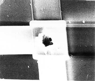
7 Resistance and the Power Distribution Problem Before After Requires fast and accurate peak current prediction Heavily influenced by packaging technology Source: Simplex

8 Electromigration (1) Limits dc-current to 1 ma/µm
9 Electromigration (2)
10 The Impact of Resistivity T r The distributed rc-line R 1 R 2 R N-1 R N C 1 C 2 C N-1 C N V in Diffused signal propagation Delay ~ L 2 voltage (V) voltage (V) x= L/10 x= L/10 x = L/4 x = L/4 x = L/2 x = L/2 x= L x= L time (nsec) time (nsec)
11 d The Global Wire Problem w w ( R C + R C R C ) T = 0.377R C Challenges No further improvements to be expected after the introduction of Copper (superconducting, optical?) Design solutions» Use of fat wires» Insert repeaters but might become prohibitive (power, area)» Efficient chip floorplanning Towards communication-based design» How to deal with latency?» Is synchronicity an absolute necessity? d out d w w out
12 Reducing RC-delay Repeater
13 Architecture Must Evolve to Fit the Landscape Global operations Low bandwidth High latency & High power 20 Clocks 90,000 tracks Local, parallel operations High bandwidth Low latency & Low power Source: Bill Dally, Stanford
14 Interconnect: # of Wiring Layers # of metal layers is steadily increasing due to: T ins ρ =2.2 µω-cm M6 Increasing die size and device count: we need more wires and longer wires to connect everything W S M5 Rising need for a hierarchical wiring network; local wires with high density and global wires with low RC H M4 3.5 Minimum Widths (Relative) 4.0 Minimum Spacing (Relative) substrate M3 M2 M1 poly 0.25 µm wiring stack µ 0.8µ 0.6µ 0.35µ 0.25µ M5 M4 M3 M2 M1 Poly µ 0.8µ 0.6µ 0.35µ 0.25µ M5 M4 M3 M2 M1 Poly
 40% reduction in resistance Electromigration improvement; 100X longer lifetime (IBM, IEDM97)» Electromigration is a limiting factor beyond 0.")
15 Interconnect Projections: Copper Copper is planned in full sub-0.25 µm process flows and large-scale designs (IBM, Motorola, IEDM97) With cladding and other effects, Cu ~2.2µΩ-cm vs. 3.5 for Al(Cu) 40% reduction in resistance Electromigration improvement; 100X longer lifetime (IBM, IEDM97)» Electromigration is a limiting factor beyond 0.18 µm if Al is used(hp, IEDM95) Vias
16 ISSUES IN TIMING
17 The Clock Skew Problem Clock Rates as High as 2 GHz in CMOS! φ t φ t φ t φ In CL1 R1 CL2 R2 CL3 R3 t i Out t l,min t l,max t r,min t r,max Clock Edge Timing Depends upon Position
18 Delay of Clock Wire R S r c C L r = 0.07 Ω/q, c = 0.04 ff/µm 2 (Tungsten wire)
19 Clock Skew
20 Constraints on Skew φ δ φ t φ t r,min + t l,min + t i t φ = t φ + δ R1 data R2 (a) Race between clock and data. φ δ φ φ + T t φ t r,max + t l,max + t i t φ + T = t φ + T + δ R1 data R2 (b) Data should be stable before clock pulse is applied.
21 Clock Constraints in Edge-Triggered Logic T δ t rmin, t rmax, + t i + + t + i t l, min t l, max δ Maximum Clock Skew Determined by Minimum Delay between Latches Minimum Clock Period Determined by Maximum Delay between Latches
22 Positive and Negative Skew φ Data CL R CL R CL R (a) Positive skew φ Data CL R CL R CL R (b) Negative skew
23 Howskewcanhelp
24 Clock Skew in Master-Slave Two Phase Design φ 1 φ 2 φ 1 φ 2 In CL1 CL2 CL3 M1 S1 M2 S2 M3 S3 φ 1
25 Clock Skew in 2-phase design new data applied to CL2 previous data latched into M2 φ 1 T φ1 φ 2 T φ12 T φ2 T φ21 φ 1 δ δ T φ12 clock period T clock overlap t min > δ -T φ12 t max > T + δ T φ12
26 How to counter Clock Skew? Negative Skew REG φ REG. REG log Out In REG φ φ Positive Skew φ Clock Distribution Data and Clock Routing
27 Clock Distribution CLOCK H-Tree Network Observe: Only Relative Skew is Important
28 Clock Network with Distributed Buffering Local Area Module Module secondary clock drivers Module Module Module Module main clock driver CLOCK Reduces absolute delay, and makes Power-Down easier Sensitive to variations in Buffer Delay
29 Example: DEC Alpha Clock Frequency: 300 MHz Million Transistors Total Clock Load: 3.75 nf Power in Clock Distribution network : 20 W (out of 50) Uses Two Level Clock Distribution: Single 6-stage driver at center of chip Secondary buffers drive left and right side clock grid in Metal3 and Metal4 Total driver size: 58 cm!
30 21164 Clocking t rise = 0.35ns t cycle = 3.3ns Clock waveform final drivers pre-driver Location of clock driver on die t skew = 150ps 2 phase single wire clock, distributed globally 2 distributed driver channels» Reduced RC delay/skew» Improved thermal distribution» 3.75nF clock load» 58 cm final driver width Local inverters for latching Conditional clocks in caches to reduce power More complex race checking Device variation

31 Clock Drivers

32 Clock Skew in Alpha Processor
33 EV6 Clocking t cycle =1.67ns t rise = 0.35ns Global clock waveform t skew =50ps PLL 2 Phase, with multiple conditional buffered clocks» 2.8 nf clock load» 40 cm final driver width Local clocks can be gated off to save power Reduced load/skew Reduced thermal issues Multiple clocks complicate race checking


34 EV6 Clock Results ps ps GCLK Skew (at Vdd/2 Crossings) GCLK Rise Times (20% to 80% Extrapolated to 0% to 100%)
35 EV7 Clock Hierarchy Active Skew Management and Multiple Clock Domains NCLK (Mem Ctrl) + widely dispersed drivers DLL DLL DLL + DLLs compensate static and lowfrequency variation + divides design and verification effort L2L_CLK (L2 Cache) GCLK (CPU Core) PLL L2R_CLK (L2 Cache) - DLL design and verification is added work SYSCLK + tailored clocks
Lecture 23. Dealing with Interconnect. Impact of Interconnect Parasitics
 Lecture 23 Dealing with Interconnect Impact of Interconnect Parasitics Reduce Reliability Affect Performance Classes of Parasitics Capacitive Resistive Inductive 1 INTERCONNECT Dealing with Capacitance
The Linear-Feedback Shift Register
 EECS 141 S02 Timing Project 2: A Random Number Generator R R R S 0 S 1 S 2 1 0 0 0 1 0 1 0 1 1 1 0 1 1 1 0 1 1 0 0 1 1 0 0 The Linear-Feedback Shift Register 1 Project Goal Design a 4-bit LFSR SPEED, SPEED,
EE115C Winter 2017 Digital Electronic Circuits. Lecture 19: Timing Analysis
 EE115C Winter 2017 Digital Electronic Circuits Lecture 19: Timing Analysis Outline Timing parameters Clock nonidealities (skew and jitter) Impact of Clk skew on timing Impact of Clk jitter on timing Flip-flop-
Xarxes de distribució del senyal de. interferència electromagnètica, consum, soroll de conmutació.
 Xarxes de distribució del senyal de rellotge. Clock skew, jitter, interferència electromagnètica, consum, soroll de conmutació. (transparències generades a partir de la presentació de Jan M. Rabaey, Anantha
Announcements. EE141- Fall 2002 Lecture 25. Interconnect Effects I/O, Power Distribution
 - Fall 2002 Lecture 25 Interconnect Effects I/O, Power Distribution Announcements Homework 9 due next Tuesday Hardware lab this week Project phase 2 due in two weeks 1 Today s Lecture Impact of interconnects»
Timing Issues. Digital Integrated Circuits A Design Perspective. Jan M. Rabaey Anantha Chandrakasan Borivoje Nikolić. January 2003
 Digital Integrated Circuits A Design Perspective Jan M. Rabaey Anantha Chandrakasan Borivoje Nikolić Timing Issues January 2003 1 Synchronous Timing CLK In R Combinational 1 R Logic 2 C in C out Out 2
Clock signal in digital circuit is responsible for synchronizing the transfer to the data between processing elements.
 1 2 Introduction Clock signal in digital circuit is responsible for synchronizing the transfer to the data between processing elements. Defines the precise instants when the circuit is allowed to change
GMU, ECE 680 Physical VLSI Design 1
 ECE680: Physical VLSI Design Chapter VII Timing Issues in Digital Circuits (chapter 10 in textbook) GMU, ECE 680 Physical VLSI Design 1 Synchronous Timing (Fig. 10 1) CLK In R Combinational 1 R Logic 2
CMPEN 411 VLSI Digital Circuits Spring 2012 Lecture 17: Dynamic Sequential Circuits And Timing Issues
 CMPEN 411 VLSI Digital Circuits Spring 2012 Lecture 17: Dynamic Sequential Circuits And Timing Issues [Adapted from Rabaey s Digital Integrated Circuits, Second Edition, 2003 J. Rabaey, A. Chandrakasan,
Clocking Issues: Distribution, Energy
 EE M216A.:. Fall 2010 Lecture 12 Clocking Issues: istribution, Energy Prof. ejan Marković ee216a@gmail.com Clock istribution Goals: eliver clock to all memory elements with acceptable skew eliver clock
10/16/2008 GMU, ECE 680 Physical VLSI Design
 ECE680: Physical VLSI Design Chapter VI Coping with Interconnect 1 Impact of Interconnect Parasitics Reduce Robustness Affect Performance Increase delay Increase power dissipation Classes of Parasitics
Lecture 9: Clocking, Clock Skew, Clock Jitter, Clock Distribution and some FM
 Lecture 9: Clocking, Clock Skew, Clock Jitter, Clock Distribution and some FM Mark McDermott Electrical and Computer Engineering The University of Texas at Austin 9/27/18 VLSI-1 Class Notes Why Clocking?
Interconnect s Role in Deep Submicron. Second class to first class
 Interconnect s Role in Deep Submicron Dennis Sylvester EE 219 November 3, 1998 Second class to first class Interconnect effects are no longer secondary # of wires # of devices More metal levels RC delay
Interconnects. Wire Resistance Wire Capacitance Wire RC Delay Crosstalk Wire Engineering Repeaters. ECE 261 James Morizio 1
 Interconnects Wire Resistance Wire Capacitance Wire RC Delay Crosstalk Wire Engineering Repeaters ECE 261 James Morizio 1 Introduction Chips are mostly made of wires called interconnect In stick diagram,
CSE241 VLSI Digital Circuits Winter Lecture 07: Timing II
 CSE241 VLSI Digital Circuits Winter 2003 Lecture 07: Timing II CSE241 L3 ASICs.1 Delay Calculation Cell Fall Cap\Tr 0.05 0.2 0.5 0.01 0.02 0.16 0.30 0.5 2.0 0.04 0.32 0.178 0.08 0.64 0.60 1.20 0.1ns 0.147ns
Lecture 21: Packaging, Power, & Clock
 Lecture 21: Packaging, Power, & Clock Outline Packaging Power Distribution Clock Distribution 2 Packages Package functions Electrical connection of signals and power from chip to board Little delay or
Next, we check the race condition to see if the circuit will work properly. Note that the minimum logic delay is a single sum.
 UNIVERSITY OF CALIFORNIA College of Engineering Department of Electrical Engineering and Computer Sciences Last modified on May 1, 2003 by Dejan Markovic (dejan@eecs.berkeley.edu) Prof. Jan Rabaey EECS
Interconnects. Introduction
 Interconnects Wire Resistance Wire Capacitance Wire RC Delay Crosstalk Wire Engineering Repeaters ECE 261 Krish Chakrabarty 1 Introduction Chips are mostly made of ires called interconnect In stick diagram,
Interconnect (2) Buffering Techniques.Transmission Lines. Lecture Fall 2003
 Buffering Techniques.Transmission Lines. Lecture Fall 2003") Interconnect (2) Buffering Techniques.Transmission Lines Lecture 12 18-322 Fall 2003 A few announcements Partners Lab Due Times Midterm 1 is nearly here Date: 10/14/02, time: 3:00-4:20PM, place: in class
Interconnect (2) Buffering Techniques.Transmission Lines Lecture 12 18-322 Fall 2003 A few announcements Partners Lab Due Times Midterm 1 is nearly here Date: 10/14/02, time: 3:00-4:20PM, place: in class
INTEGRATED CIRCUITS. For a complete data sheet, please also download:
 INTEGRATED CIRCUITS DATA SHEET For a complete data sheet, please also download: The IC6 74HC/HCT/HCU/HCMOS Logic Family Specifications The IC6 74HC/HCT/HCU/HCMOS Logic Package Information The IC6 74HC/HCT/HCU/HCMOS
Lecture 6 Power Zhuo Feng. Z. Feng MTU EE4800 CMOS Digital IC Design & Analysis 2010
 EE4800 CMOS Digital IC Design & Analysis Lecture 6 Power Zhuo Feng 6.1 Outline Power and Energy Dynamic Power Static Power 6.2 Power and Energy Power is drawn from a voltage source attached to the V DD
Topics to be Covered. capacitance inductance transmission lines
 Topics to be Covered Circuit Elements Switching Characteristics Power Dissipation Conductor Sizes Charge Sharing Design Margins Yield resistance capacitance inductance transmission lines Resistance of
ESE 570: Digital Integrated Circuits and VLSI Fundamentals
 ESE 570: Digital Integrated Circuits and VLSI Fundamentals Lec 19: March 29, 2018 Memory Overview, Memory Core Cells Today! Charge Leakage/Charge Sharing " Domino Logic Design Considerations! Logic Comparisons!
VLSI GATE LEVEL DESIGN UNIT - III P.VIDYA SAGAR ( ASSOCIATE PROFESSOR) Department of Electronics and Communication Engineering, VBIT
 Department of Electronics and Communication Engineering, VBIT") VLSI UNIT - III GATE LEVEL DESIGN P.VIDYA SAGAR ( ASSOCIATE PROFESSOR) contents GATE LEVEL DESIGN : Logic Gates and Other complex gates, Switch logic, Alternate gate circuits, Time Delays, Driving large
VLSI UNIT - III GATE LEVEL DESIGN P.VIDYA SAGAR ( ASSOCIATE PROFESSOR) contents GATE LEVEL DESIGN : Logic Gates and Other complex gates, Switch logic, Alternate gate circuits, Time Delays, Driving large
Luis Manuel Santana Gallego 31 Investigation and simulation of the clock skew in modern integrated circuits
 Luis Manuel Santana Gallego 31 Investigation and simulation of the clock skew in modern egrated circuits 3. Clock skew 3.1. Definitions For two sequentially adjacent registers, as shown in figure.1, C
Digital System Clocking: High-Performance and Low-Power Aspects. Vojin G. Oklobdzija, Vladimir M. Stojanovic, Dejan M. Markovic, Nikola M.
 Digital System Clocking: High-Performance and Low-Power Aspects Vojin G. Oklobdzija, Vladimir M. Stojanovic, Dejan M. Markovic, Nikola M. Nedovic Wiley-Interscience and IEEE Press, January 2003 Nov. 14,
EEC 216 Lecture #3: Power Estimation, Interconnect, & Architecture. Rajeevan Amirtharajah University of California, Davis
 EEC 216 Lecture #3: Power Estimation, Interconnect, & Architecture Rajeevan Amirtharajah University of California, Davis Outline Announcements Review: PDP, EDP, Intersignal Correlations, Glitching, Top
EECS 151/251A Homework 5
 EECS 151/251A Homework 5 Due Monday, March 5 th, 2018 Problem 1: Timing The data-path shown below is used in a simple processor. clk rd1 rd2 0 wr regfile 1 0 ALU REG 1 The elements used in the design have
EE241 - Spring 2006 Advanced Digital Integrated Circuits
 EE241 - Spring 2006 Advanced Digital Integrated Circuits Lecture 20: Asynchronous & Synchronization Self-timed and Asynchronous Design Functions of clock in synchronous design 1) Acts as completion signal
! Charge Leakage/Charge Sharing. " Domino Logic Design Considerations. ! Logic Comparisons. ! Memory. " Classification. " ROM Memories.
 ESE 57: Digital Integrated Circuits and VLSI Fundamentals Lec 9: March 9, 8 Memory Overview, Memory Core Cells Today! Charge Leakage/ " Domino Logic Design Considerations! Logic Comparisons! Memory " Classification
ESE 570: Digital Integrated Circuits and VLSI Fundamentals
 ESE 570: Digital Integrated Circuits and VLSI Fundamentals Lec 23: April 17, 2018 I/O Circuits, Inductive Noise, CLK Generation Lecture Outline! Packaging! Variation and Testing! I/O Circuits! Inductive
Digital VLSI Design. Lecture 8: Clock Tree Synthesis
 Digital VLSI Design Lecture 8: Clock Tree Synthesis Semester A, 2018-19 Lecturer: Dr. Adam Teman January 12, 2019 Disclaimer: This course was prepared, in its entirety, by Adam Teman. Many materials were
Lecture 9: Interconnect
 Digital Integrated Circuits (83-313) Lecture 9: Interconnect Semester B, 2016-17 Lecturer: Dr. Adam Teman TAs: Itamar Levi, Robert Giterman 23 May 2017 Disclaimer: This course was prepared, in its entirety,
The Wire. Digital Integrated Circuits A Design Perspective. Jan M. Rabaey Anantha Chandrakasan Borivoje Nikolic. July 30, 2002
 Digital Integrated Circuits A Design Perspective Jan M. Rabaey Anantha Chandrakasan Borivoje Nikolic The Wire July 30, 2002 1 The Wire transmitters receivers schematics physical 2 Interconnect Impact on
Semiconductor memories
 Semiconductor memories Semiconductor Memories Data in Write Memory cell Read Data out Some design issues : How many cells? Function? Power consuption? Access type? How fast are read/write operations? Semiconductor
Dynamic Repeater with Booster Enhancement for Fast Switching Speed and Propagation in Long Interconnect
 Wright State University CORE Scholar Browse all Theses and Dissertations Theses and Dissertations 2014 Dynamic Repeater with Booster Enhancement for Fast Switching Speed and Propagation in Long Interconnect
EE141-Spring 2007 Digital Integrated Circuits. Administrative Stuff. Last Lecture. Wires. Interconnect Impact on Chip. The Wire
 EE141-Spring 2007 Digital Integrated Circuits ecture 10 Administrative Stuff No ab this week Midterm 1 on Tu! HW5 to be posted by next Friday Due Fr. March 2 5pm Introduction to wires 1 2 ast ecture ast
Lecture 5: DC & Transient Response
 Lecture 5: DC & Transient Response Outline q Pass Transistors q DC Response q Logic Levels and Noise Margins q Transient Response q RC Delay Models q Delay Estimation 2 Activity 1) If the width of a transistor
CMPEN 411. Spring Lecture 18: Static Sequential Circuits
 CMPEN 411 VLSI Digital Circuits Spring 2011 Lecture 18: Static Sequential Circuits [Adapted from Rabaey s Digital Integrated Circuits, Second Edition, 2003 J. Rabaey, A. Chandrakasan, B. Nikolic] Sp11
EE 560 CHIP INPUT AND OUTPUT (I/0) CIRCUITS. Kenneth R. Laker, University of Pennsylvania
 CIRCUITS. Kenneth R. Laker, University of Pennsylvania") 1 EE 560 CHIP INPUT AND OUTPUT (I/0) CIRCUITS 2 -> ESD PROTECTION CIRCUITS (INPUT PADS) -> ON-CHIP CLOCK GENERATION & DISTRIBUTION -> OUTPUT PADS -> ON-CHIP NOISE DUE TO PARASITIC INDUCTANCE -> SUPER BUFFER
1 EE 560 CHIP INPUT AND OUTPUT (I/0) CIRCUITS 2 -> ESD PROTECTION CIRCUITS (INPUT PADS) -> ON-CHIP CLOCK GENERATION & DISTRIBUTION -> OUTPUT PADS -> ON-CHIP NOISE DUE TO PARASITIC INDUCTANCE -> SUPER BUFFER
Lecture 15: Scaling & Economics
 Lecture 15: Scaling & Economics Outline Scaling Transistors Interconnect Future Challenges Economics 2 Moore s Law Recall that Moore s Law has been driving CMOS [Moore65] Corollary: clock speeds have improved
Digital Integrated Circuits (83-313) Lecture 5: Interconnect. Semester B, Lecturer: Adam Teman TAs: Itamar Levi, Robert Giterman 1
 Lecture 5: Interconnect. Semester B, Lecturer: Adam Teman TAs: Itamar Levi, Robert Giterman 1") Digital Integrated Circuits (83-313) Lecture 5: Interconnect Semester B, 2015-16 Lecturer: Adam Teman TAs: Itamar Levi, Robert Giterman 1 What will we learn today? 1 A First Glance at Interconnect 2 3
Digital Integrated Circuits (83-313) Lecture 5: Interconnect Semester B, 2015-16 Lecturer: Adam Teman TAs: Itamar Levi, Robert Giterman 1 What will we learn today? 1 A First Glance at Interconnect 2 3
EE141-Spring 2008 Digital Integrated Circuits EE141. Announcements EECS141 EE141. Lecture 24: Wires
 EE141-Spring 2008 Digital Integrated Circuits Lecture 24: Wires 1 Announcements Hw 8 posted last graded homework Project phase II feedback to be expected anytime 2 Material Last Lecture: Wire capacitance
THE INVERTER. Inverter
 THE INVERTER DIGITAL GATES Fundamental Parameters Functionality Reliability, Robustness Area Performance» Speed (delay)» Power Consumption» Energy Noise in Digital Integrated Circuits v(t) V DD i(t) (a)
CMPEN 411 VLSI Digital Circuits Spring 2012
 CMPEN 411 VLSI Digital Circuits Spring 2012 Lecture 09: Resistance & Inverter Dynamic View [Adapted from Rabaey s Digital Integrated Circuits, Second Edition, 2003 J. Rabaey, A. Chandrakasan, B. Nikolic]
ESE 570: Digital Integrated Circuits and VLSI Fundamentals
 ESE 570: Digital Integrated Circuits and VLSI Fundamentals Lec 21: April 4, 2017 Memory Overview, Memory Core Cells Penn ESE 570 Spring 2017 Khanna Today! Memory " Classification " ROM Memories " RAM Memory
CARNEGIE MELLON UNIVERSITY DEPARTMENT OF ELECTRICAL AND COMPUTER ENGINEERING DIGITAL INTEGRATED CIRCUITS FALL 2002
 CARNEGIE MELLON UNIVERSITY DEPARTMENT OF ELECTRICAL AND COMPUTER ENGINEERING 18-322 DIGITAL INTEGRATED CIRCUITS FALL 2002 Final Examination, Monday Dec. 16, 2002 NAME: SECTION: Time: 180 minutes Closed
ECE 497 JS Lecture - 18 Impact of Scaling
 ECE 497 JS Lecture - 18 Impact of Scaling Spring 2004 Jose E. Schutt-Aine Electrical & Computer Engineering University of Illinois jose@emlab.uiuc.edu 1 Announcements Thursday April 8 th Speaker: Prof.
INTEGRATED CIRCUITS. For a complete data sheet, please also download:
 INTEGRATED CIRCUITS DATA SHEET For a complete data sheet, please also download: The IC06 74HC/HCT/HCU/HCMOS Logic Family Specifications The IC06 74HC/HCT/HCU/HCMOS Logic Package Information The IC06 74HC/HCT/HCU/HCMOS
CMOS logic gates. João Canas Ferreira. March University of Porto Faculty of Engineering
 CMOS logic gates João Canas Ferreira University of Porto Faculty of Engineering March 2016 Topics 1 General structure 2 General properties 3 Cell layout João Canas Ferreira (FEUP) CMOS logic gates March
Chapter 5 CMOS Logic Gate Design
 Chapter 5 CMOS Logic Gate Design Section 5. -To achieve correct operation of integrated logic gates, we need to satisfy 1. Functional specification. Temporal (timing) constraint. (1) In CMOS, incorrect
EE241 - Spring 2000 Advanced Digital Integrated Circuits. Announcements
 EE241 - Spring 2000 Advanced Digital Integrated Circuits Lecture 3 Circuit Optimization for Speed Announcements Tu 2/8/00 class will be pre-taped on Friday, 2/4, 4-5:30 203 McLaughlin Class notes are available
Skew-Tolerant Circuit Design
 Skew-Tolerant Circuit Design David Harris David_Harris@hmc.edu December, 2000 Harvey Mudd College Claremont, CA Outline Introduction Skew-Tolerant Circuits Traditional Domino Circuits Skew-Tolerant Domino
UNIVERSITY OF CALIFORNIA College of Engineering Department of Electrical Engineering and Computer Sciences. Professor Oldham Fall 1999
 UNIVERSITY OF CLIFORNI College of Engineering Department of Electrical Engineering and Computer Sciences Professor Oldham Fall 1999 EECS 40 FINL EXM 13 December 1999 Name: Last, First Student ID: T: Kusuma
Digital Integrated Circuits A Design Perspective. Semiconductor. Memories. Memories
 Digital Integrated Circuits A Design Perspective Semiconductor Chapter Overview Memory Classification Memory Architectures The Memory Core Periphery Reliability Case Studies Semiconductor Memory Classification
Clock Strategy. VLSI System Design NCKUEE-KJLEE
 Clock Strategy Clocked Systems Latch and Flip-flops System timing Clock skew High speed latch design Phase locked loop ynamic logic Multiple phase Clock distribution Clocked Systems Most VLSI systems are
Lecture 12 CMOS Delay & Transient Response
 EE 471: Transport Phenomena in Solid State Devices Spring 2018 Lecture 12 CMOS Delay & Transient Response Bryan Ackland Department of Electrical and Computer Engineering Stevens Institute of Technology
Hw 6 and 7 Graded and available Project Phase 2 Graded Project Phase 3 Launch Today
 EECS141 1 Hw 8 Posted Last one to be graded Due Friday April 30 Hw 6 and 7 Graded and available Project Phase 2 Graded Project Phase 3 Launch Today EECS141 2 1 6 5 4 3 2 1 0 1.5 2 2.5 3 3.5 4 Frequency
Lecture 16: Circuit Pitfalls
 Introduction to CMOS VLSI Design Lecture 16: Circuit Pitfalls David Harris Harvey Mudd College Spring 2004 Outline Pitfalls Detective puzzle Given circuit and symptom, diagnose cause and recommend solution
INTEGRATED CIRCUITS. For a complete data sheet, please also download:
 INTEGRATED CIRCUITS DATA SEET For a complete data sheet, please also download: The IC0 74C/CT/CU/CMOS ogic Family Specifications The IC0 74C/CT/CU/CMOS ogic Package Information The IC0 74C/CT/CU/CMOS ogic
Digital Integrated Circuits A Design Perspective
 Digital Integrated Circuits A Design Perspective Jan M. Rabaey Anantha Chandrakasan Borivoje Nikolic Designing Sequential Logic Circuits November 2002 Sequential Logic Inputs Current State COMBINATIONAL
Very Large Scale Integration (VLSI)
") Very Large Scale Integration (VLSI) Lecture 4 Dr. Ahmed H. Madian Ah_madian@hotmail.com Dr. Ahmed H. Madian-VLSI Contents Delay estimation Simple RC model Penfield-Rubenstein Model Logical effort Delay
Very Large Scale Integration (VLSI) Lecture 4 Dr. Ahmed H. Madian Ah_madian@hotmail.com Dr. Ahmed H. Madian-VLSI Contents Delay estimation Simple RC model Penfield-Rubenstein Model Logical effort Delay
ESE 570: Digital Integrated Circuits and VLSI Fundamentals
 ESE 570: Digital Integrated Circuits and VLSI Fundamentals Lec 24: April 19, 2018 Crosstalk and Wiring, Transmission Lines Lecture Outline! Crosstalk! Repeaters in Wiring! Transmission Lines " Where transmission
Chapter Overview. Memory Classification. Memory Architectures. The Memory Core. Periphery. Reliability. Memory
 SRAM Design Chapter Overview Classification Architectures The Core Periphery Reliability Semiconductor Classification RWM NVRWM ROM Random Access Non-Random Access EPROM E 2 PROM Mask-Programmed Programmable
MODULE III PHYSICAL DESIGN ISSUES
 VLSI Digital Design MODULE III PHYSICAL DESIGN ISSUES 3.2 Power-supply and clock distribution EE - VDD -P2006 3:1 3.1.1 Power dissipation in CMOS gates Power dissipation importance Package Cost. Power
Timing Analysis with Clock Skew
 , Mark Horowitz 1, & Dean Liu 1 David_Harris@hmc.edu, {horowitz, dliu}@vlsi.stanford.edu March, 1999 Harvey Mudd College Claremont, CA 1 (with Stanford University, Stanford, CA) Outline Introduction Timing
Digital Integrated Circuits. The Wire * Fuyuzhuo. *Thanks for Dr.Guoyong.SHI for his slides contributed for the talk. Digital IC.
 Digital Integrated Circuits The Wire * Fuyuzhuo *Thanks for Dr.Guoyong.SHI for his slides contributed for the talk Introduction The Wire transmitters receivers schematics physical 2 Interconnect Impact
ECE321 Electronics I
 ECE31 Electronics Lecture 1: CMOS nverter: Noise Margin & Delay Model Payman Zarkesh-Ha Office: ECE Bldg. 30B Office hours: Tuesday :00-3:00PM or by appointment E-mail: payman@ece.unm.edu Slide: 1 CMOS
! Crosstalk. ! Repeaters in Wiring. ! Transmission Lines. " Where transmission lines arise? " Lossless Transmission Line.
 ESE 570: Digital Integrated Circuits and VLSI Fundamentals Lec 24: April 19, 2018 Crosstalk and Wiring, Transmission Lines Lecture Outline! Crosstalk! Repeaters in Wiring! Transmission Lines " Where transmission
Homework Assignment #5 EE 477 Spring 2017 Professor Parker
 Homework Assignment #5 EE 477 Spring 2017 Professor Parker Question 1: (15%) Compute the worst-case rising and falling RC time constants at point B of the circuit below using the Elmore delay method. Assume
ECE 342 Electronic Circuits. Lecture 35 CMOS Delay Model
 ECE 34 Electronic Circuits Lecture 35 CMOS Delay Model Jose E. Schutt-Aine Electrical & Computer Engineering University of Illinois jesa@illinois.edu ECE 34 Jose Schutt Aine 1 Digital Circuits V IH : Input
Semiconductor Memories
 Semiconductor References: Adapted from: Digital Integrated Circuits: A Design Perspective, J. Rabaey UCB Principles of CMOS VLSI Design: A Systems Perspective, 2nd Ed., N. H. E. Weste and K. Eshraghian
Digital Logic Design - Chapter 4
 Digital Logic Design - Chapter 4 1. Analyze the latch circuit shown below by obtaining timing diagram for the circuit; include propagation delays. Y This circuit has two external input and one feedback
INTEGRATED CIRCUITS. For a complete data sheet, please also download:
 INTEGRATED CIRCUITS DATA SHEET For a complete data sheet, please also download: The IC06 74HC/HCT/HCU/HCMOS Logic Family Specifications The IC06 74HC/HCT/HCU/HCMOS Logic Package Information The IC06 74HC/HCT/HCU/HCMOS
UNISONIC TECHNOLOGIES CO., LTD L16B45 Preliminary CMOS IC
 UNISONIC TECHNOLOGIES CO., LTD L16B45 Preliminary CMOS IC 16-BIT CONSTANT CURRENT LED SINK DRIVER DESCRIPTION The UTC L16B45 is designed for LED displays. UTC L16B45 contains a serial buffer and data latches
Step 1. Finding V M. Goal: Þnd V M = input voltage for the output = V M both transistors are saturated at V IN = V M since
 Step 1. Finding V M Goal: Þnd V M = input voltage for the output = V M both transistors are saturated at V IN = V M since V DSn = V M - 0 > V M - V Tn V SDp = V DD - V M = (V DD - V M ) V Tp Equate drain
VLSI Design, Fall Logical Effort. Jacob Abraham
 6. Logical Effort 6. Logical Effort Jacob Abraham Department of Electrical and Computer Engineering The University of Texas at Austin VLSI Design Fall 207 September 20, 207 ECE Department, University of
ECE 497 JS Lecture - 12 Device Technologies
 ECE 497 JS Lecture - 12 Device Technologies Spring 2004 Jose E. Schutt-Aine Electrical & Computer Engineering University of Illinois jose@emlab.uiuc.edu 1 NMOS Transistor 2 ρ Source channel charge density
Spiral 2 7. Capacitance, Delay and Sizing. Mark Redekopp
 2-7.1 Spiral 2 7 Capacitance, Delay and Sizing Mark Redekopp 2-7.2 Learning Outcomes I understand the sources of capacitance in CMOS circuits I understand how delay scales with resistance, capacitance
Digital Integrated Circuits A Design Perspective
 Semiconductor Memories Adapted from Chapter 12 of Digital Integrated Circuits A Design Perspective Jan M. Rabaey et al. Copyright 2003 Prentice Hall/Pearson Outline Memory Classification Memory Architectures
Itanium TM Processor Clock Design
 Itanium TM Processor Design Utpal Desai 1, Simon Tam, Robert Kim, Ji Zhang, Stefan Rusu Intel Corporation, M/S SC12-502, 2200 Mission College Blvd, Santa Clara, CA 95052 ABSTRACT The Itanium processor
EE 466/586 VLSI Design. Partha Pande School of EECS Washington State University
 EE 466/586 VLSI Design Partha Pande School of EECS Washington State University pande@eecs.wsu.edu Lecture 8 Power Dissipation in CMOS Gates Power in CMOS gates Dynamic Power Capacitance switching Crowbar
INTEGRATED CIRCUITS. For a complete data sheet, please also download:
 INTEGRATED CIRCUITS DATA SHEET For a complete data sheet, please also download: The IC6 74HC/HCT/HCU/HCMOS ogic Family Specifications The IC6 74HC/HCT/HCU/HCMOS ogic Package Information The IC6 74HC/HCT/HCU/HCMOS
Managing Physical Design Issues in ASIC Toolflows Complex Digital Systems Christopher Batten February 21, 2006
 Managing Physical Design Issues in ASI Toolflows 6.375 omplex Digital Systems hristopher Batten February 1, 006 Managing Physical Design Issues in ASI Toolflows Logical Effort Physical Design Issues lock
EE241 - Spring 2003 Advanced Digital Integrated Circuits
 EE241 - Spring 2003 Advanced Digital Integrated Circuits Lecture 16 Energy-Recovery Circuits SOI Technology and Circuits Optimal EDP Contours 1 Leakage and Switching ELk 2 = ESw Opt L ln d K tech α avg
Lecture 16: Circuit Pitfalls
 Lecture 16: Circuit Pitfalls Outline Variation Noise Budgets Reliability Circuit Pitfalls 2 Variation Process Threshold Channel length Interconnect dimensions Environment Voltage Temperature Aging / Wearout
EEE 421 VLSI Circuits
 EEE 421 CMOS Properties Full rail-to-rail swing high noise margins» Logic levels not dependent upon the relative device sizes transistors can be minimum size ratioless Always a path to V dd or GND in steady
Designing Sequential Logic Circuits
 igital Integrated Circuits (83-313) Lecture 5: esigning Sequential Logic Circuits Semester B, 2016-17 Lecturer: r. Adam Teman TAs: Itamar Levi, Robert Giterman 26 April 2017 isclaimer: This course was
CMOS Inverter. Performance Scaling
 Announcements Exam #2 regrade requests due today. Homework #8 due today. Final Exam: Th June 12, 8:30 10:20am, CMU 120 (extension to 11:20am requested). Grades available for viewing via Catalyst. CMOS
Lecture 5: DC & Transient Response
 Lecture 5: DC & Transient Response Outline Pass Transistors DC Response Logic Levels and Noise Margins Transient Response RC Delay Models Delay Estimation 2 Pass Transistors We have assumed source is grounded
EECS 151/251A Spring 2018 Digital Design and Integrated Circuits. Instructors: Nick Weaver & John Wawrzynek. Lecture 12 EE141
 EECS 151/251A Spring 2018 Digital Design and Integrated Circuits Instructors: Nick Weaver & John Wawrzynek Lecture 12 1 Wire Models All-inclusive model Capacitance-only 2 Capacitance Capacitance: The Parallel
Adding a New Dimension to Physical Design. Sachin Sapatnekar University of Minnesota
 Adding a New Dimension to Physical Design Sachin Sapatnekar University of Minnesota 1 Outline What is 3D about? Why 3D? 3D-specific challenges 3D analysis and optimization 2 Planning a city: Land usage
Scaling of MOS Circuits. 4. International Technology Roadmap for Semiconductors (ITRS) 6. Scaling factors for device parameters
 6. Scaling factors for device parameters") 1 Scaling of MOS Circuits CONTENTS 1. What is scaling?. Why scaling? 3. Figure(s) of Merit (FoM) for scaling 4. International Technology Roadmap for Semiconductors (ITRS) 5. Scaling models 6. Scaling factors
1 Scaling of MOS Circuits CONTENTS 1. What is scaling?. Why scaling? 3. Figure(s) of Merit (FoM) for scaling 4. International Technology Roadmap for Semiconductors (ITRS) 5. Scaling models 6. Scaling factors
SEMICONDUCTOR MEMORIES
 SEMICONDUCTOR MEMORIES Semiconductor Memory Classification RWM NVRWM ROM Random Access Non-Random Access EPROM E 2 PROM Mask-Programmed Programmable (PROM) SRAM FIFO FLASH DRAM LIFO Shift Register CAM
INTEGRATED CIRCUITS. For a complete data sheet, please also download:
 INTEGRATED CIRCUITS DATA SEET For a complete data sheet, please also download: The IC6 74C/CT/CU/CMOS ogic Family Specifications The IC6 74C/CT/CU/CMOS ogic Package Information The IC6 74C/CT/CU/CMOS ogic
Power Consumption in CMOS CONCORDIA VLSI DESIGN LAB
 Power Consumption in CMOS 1 Power Dissipation in CMOS Two Components contribute to the power dissipation:» Static Power Dissipation Leakage current Sub-threshold current» Dynamic Power Dissipation Short
Issues on Timing and Clocking
 ECE152B TC 1 Issues on Timing and Clocking X Combinational Logic Z... clock clock clock period ECE152B TC 2 Latch and Flip-Flop L CK CK 1 L1 1 L2 2 CK CK CK ECE152B TC 3 Clocking X Combinational Logic...
NTE4035B Integrated Circuit CMOS, 4 Bit Parallel In/Parallel Out Shift Register
 NTE4035B Integrated Circuit CMOS, 4 Bit Parallel In/Parallel Out Shift Register Description: The NTE4035B is a 4 bit shift register in a 16 Lead DIP type package constructed with MOS P Channel an N Channel
MOSIS REPORT. Spring MOSIS Report 1. MOSIS Report 2. MOSIS Report 3
 MOSIS REPORT Spring 2010 MOSIS Report 1 MOSIS Report 2 MOSIS Report 3 MOSIS Report 1 Design of 4-bit counter using J-K flip flop I. Objective The purpose of this project is to design one 4-bit counter
EE141Microelettronica. CMOS Logic
 Microelettronica CMOS Logic CMOS logic Power consumption in CMOS logic gates Where Does Power Go in CMOS? Dynamic Power Consumption Charging and Discharging Capacitors Short Circuit Currents Short Circuit