Thermal-reliable 3D Clock-tree Synthesis Considering Nonlinear Electrical-thermal-coupled TSV Model
|
|
|
- Brice Parrish
- 5 years ago
- Views:
Transcription
1 Thermal-reliable 3D Clock-tree Synthesis Considering Nonlinear Electrical-thermal-coupled TSV Model Yang Shang 1, Chun Zhang 1, Hao Yu 1, Chuan Seng Tan 1, Xin Zhao 2, Sung Kyu Lim 2 1 School of Electrical and Electronic Engineering Nanyang Technological University, Singapore 2 GTCAD Laboratory, Georgia Institute of Technology, Atlanta. USA
2 Outline Background and Motivation Electrical-thermal-coupled TSV Model Nonlinear Optimization of Skew Reduction Experimental Results Conclusion and Future Work


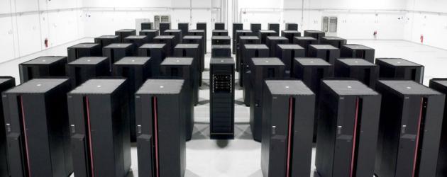


3 3D Server for Big-data Cloud Server 3D Processor Supercomputer TSVs

4 Thermal Challenges in 3D Integration Thermal reliability is concerned: large non-uniform thermal gradient as limited heat dissipation paths in 3D IC 3D clock-tree synthesis to balance electrical-thermal coupling induced skew Temperature adds up from longer heat dissipation path 3D CLK network with skew under temperature profile 80 o C 60 o C Skew: 100ps Skew: 10ps 40 o C Skew: 1ps
![Temperature Aware Clock-tree Synthesis Clock-skew reduction methods considering temperature Buffer Insertion [1] Merging point adjustment [2] Wire length balancing[3] 3D clock-skew reduction by](/docs-images/94/121712584/images/5-0.jpg "thermal TSV insertion, which requires Accurate electrical-thermal TSV model Skew balance method [1] J. Minz, X. Zhao, and S. K.")
5 Temperature Aware Clock-tree Synthesis Clock-skew reduction methods considering temperature Buffer Insertion [1] Merging point adjustment [2] Wire length balancing[3] 3D clock-skew reduction by thermal TSV insertion, which requires Accurate electrical-thermal TSV model Skew balance method [1] J. Minz, X. Zhao, and S. K. Lim, Buffered clock tree synthesis for 3d ics under thermal variations, in IEEE/ACM ASP-DAC, [2 ]M. Cho, S. Ahmed, and D. Pan, TACO: Temperature aware clock-tree optimization, in IEEE/ACM ICCAD, [3]J. Cong, A. Kahng, C. Koh, and C. A. Tsao, Bounded-skew clock and steiner routing, ACM Trans. on Design Automation of Electronic Systems, vol. 3, no. 3, pp , 1998.

6 TSV Fabrication Technology TSV material: Al/Cu, under-bump-metal TSV diameter: 1~20um TSV height: 20~50um Liner material: SiO 2 or Si 3 N 4 Liner thickness: 0.2~0.5um Simplified TSV fabrication process TSV Etch Liner Deposition TSV Fill Thinning and Stacking Tier N Tier N+1
 Depletion region exists because of the work function difference between TSV metal and silicon substrate The radius of depletion region is temperature and voltage dependent C-V")
7 Signal TSVs Signal TSVs provide electrical connection between adjacent tiers Non-linear MOS-capacitance (MOSCAP) is formed between signal TSV and substrate due to the existence of liner Low-k liner is preferred (SiO 2 ) Depletion region exists because of the work function difference between TSV metal and silicon substrate The radius of depletion region is temperature and voltage dependent C-V curve of MOSCAP
 α and β 1, β 2 are the temperature coefficients (C MIN")
8 Signal TSV Modeling RC equivalent circuit of signal TSVs r ox is the outer radius of liner, r metal is the radius of TSV, r dep is the outer radius of depletion region TSV model considering non-linear temperature effect (C MAX ) α and β 1, β 2 are the temperature coefficients (C MIN )
 Buffer without TSV Buffer with TSV 14ps Diameter: 5um Height:50um Liner:200nm PTM")
9 Signal TSV Delay Modeling Signal TSVs introduce noticed delay Process and capacitance dependent Non-linear function with temperature 66ps (200C) Buffer without TSV Buffer with TSV 14ps Diameter: 5um Height:50um Liner:200nm PTM Model
10 Nonlinear Electrical-thermal-coupled Signal TSV Delay Model Scalable signal TSV delay model where R in is the total resistance looking from C T to the input and τ 0 is the delay of circuit without C T Non-linear function of in delay model with temperature where k0, k1, k2, k3 are the temperature coefficient in different order
 Chip temperature can be reduced by adding thermal TSVs High thermal conductivity liner material is preferred (Si 3 N 4, 30W/m K ) Liner Material Dummy TSV")
11 Dummy TSVs Dummy TSVs provide additional heat dissipation paths to heat-sink as TSV metal (Cu, 400W/m K) has much larger thermal conductivity than liner (SiO 2, 1.2W/m K) Chip temperature can be reduced by adding thermal TSVs High thermal conductivity liner material is preferred (Si 3 N 4, 30W/m K ) Liner Material Dummy TSV

12 Dummy TSV Model Dummy TSV density (η) is the ratio equivalent area of thermal TSV over total chip area(a) Total thermal conductivity between chip and heat sink σ TSV and σ 0 are the chip thermal conductivity with and without TSV, respectively Equivalent Area of Thermal TSV (ηa)
13 Thermal Gradient Reduction by Dummy TSV Insertion Temperature reduction saturation effect due to dummy TSV insertion P/A is the power density, l is the equivalent length of thermal dissipation patch ΔT increases linearly with η as η is smaller than σ 0 /(σ TSV σ 0 ), ΔT is less sensitive to η when η is approaching or larger than σ 0 /(σ TSV σ 0 ), η is limited by the chip area overhead and saturation of temperature reduction effect Balanced thermal gradient will balance clock skew
14 Nonlinear OPT of 3D CLK Skew by Dummy TSV Insertion: Problem Formulation I Objective function: minimize the variance of skew in all clock branches Parameters: dummy TSV insertion density Constraints: lb is the min thermal TSV density ddetermined by the foundry process limitation ub is the max thermal TSV density determined by temperature reduction sensitivity function as well as the maximum allowed chip overhead
 Clock Tree Benchmarks Temperature Profile from Hotspot Benchmark Circuit RC Extraction T4 T5")

15 Nonlinear OPT of 3D CLK Skew by Dummy TSV Insertion: Problem Formulation II Chip Gridding (M x N) Clock Tree Benchmarks Temperature Profile from Hotspot Benchmark Circuit RC Extraction T4 T5 T3 T2 T1 Nonlinear Delay (Dk) Each grid is available for the thermal TSV insertion with density of x i, i=1є[1,mxn] Parent Node Child Node is the summation of delay of passing through all grids


16 Dummy TSV Insertion Sensitivity Sensitivity of temperature reduction w.r.t. dummy TSV density is relative chip temperature without dummy TSV insertion, is threshold density of dummy TSV. Constant sensitivity is achieved when η<<η 0. Typical: 2~10 K for 100 dummy TSVs in 1mm 2 Sensitivity is approaching zero when η>>η 0
17 Nonlinear OPT of 3D CLK Skew by Dummy TSV Insertion: Conjugate-gradient Solution Original problem is relaxed with Lagrange penalty factor to remove the inequality constraint x 0 where Conjugate gradient method iteratively searches along the gradient drop reduction to find the x which minimizes f (x). Problem is solved multiple times with properly selected x 0 to avoid local minimum x' x 0 ' x
18 Nonlinear Electrical-thermal Coupling by Signal TSVs Nonlinear temperature-dependent TSV capacitance Nonlinear temperature-dependent TSV delay Linear Model Reference Measurement result [4] shows non-linear TSV capacitance Delay introduced by non-linear TSV model shows large difference from linear model at high temperature [4] G. Katti and et al., Temperature dependent electrical characteristics of through-si-via (tsv) interconnections, in IITC, 2010.

19 Temperature Reduction by Dummy TSVs COMSOL multi-physics simulator for thermal analysis A 4-tier 3D-IC test case : Tier thickness: 40µ m; Thermal TSV has a diameter of 15µ m; Heat sink conductance: W/(K m 2 ) Chip temperature is linearly reduced by increasing thermal TSV density


 based 3d ics, IEEE")
20 Dummy TSV Insertion for 3D Clock Skew Reduction: Set-up I Two generalized 4-Tier 3D IC H-Trees designed IBM clock-tree benchmarks r1- r5 [5] synthesized to 4-tier 3D clock-tree [6] 3D-IC chip divided into 64x64 grids for dummytsv insertion H-Tree 1 (14TSV location) H-Tree 2 (28TSV location) [5] Ibm clock tree benchmarks, [6] X. Zhao, J. Minz, and S. K. Lim, Low-power and reliable clock network design for through-silicon via (tsv) based 3d ics, IEEE Trans. on Components, Packaging, and Manufacturing Technology, vol. 1, no. 2, pp , feb 2011.


![average input of all SPEC2000 benchmarks [8]](/docs-images/94/121712584/images/21-2.jpg "Maximal thermal TSV density is limited to be lower")


21 Dummy TSV Insertion for 3D Clock Skew Reduction: Set-up II HotSpot [7] is used to extract the temperature distribution at each location Temperature distribution is calculated from the average input of all SPEC2000 benchmarks [8] Maximal thermal TSV density is limited to be lower than 7% of the local grid area. Different signal TSV-bundles T2,T4, T8 and T10 are deployed with number of 2, 4, 8 and 10 TSVs 3D Clock Tree of r5 [7] Hotspot: [8]


22 Dummy TSV Insertion for 3D Clock Skew Reduction: Result I H-Tree 1 clock skew comparison before and after TSV insertion Temperature profile before TSV insertion Tem After TSV insertion
23 Dummy TSV Insertion for 3D Clock Skew Reduction: Result II Synthesized 3D Clock Tree of Benchmark r5 Tier 0 Tier 2 Tier 1 Tier 3
24 Dummy TSV Insertion for 3D Clock Skew Reduction: Result III htree1 (14 Signal TSV locations) Type Orig Lin Impr% Time(s) Nonlin Impr% Time(s) T % % T % % 57.9 T % % T % % Mean % % htree2 (28 Signal TSV locations) Type Orig Lin Impr% Time(s) Nonlin Impr% Time(s) T % % T % % T % % T % % Mean % % r1 (45 Signal TSV locations) Type Orig Lin Impr% Time(s) Nonlin Impr% Time(s) T % % T % % T % % T % % Mean % % r2 (60 Signal TSV locations) Type Orig Lin Impr% Time(s) Nonlin Impr% Time(s) T % % 389 T % % T % % T % % Mean % % r3 (75 Signal TSV locations) Type Orig Lin Impr% Time(s) Nonlin Impr% Time(s) T % % T % % 451 T % % T % % Mean % % r4 (90 Signal TSV locations) Type Orig Lin Impr% Time(s) Nonlin Impr% Time(s) T % % T % % T % % T % % Mean % % r5 (90 Signal TSV locations) Type Orig Lin Impr% Time(s) Nonlin Impr% Time(s) T % % 1963 T % % 1716 T % % 1694 T % % 1750 Mean % % 1781 Overall 46.8% 58.4% 58.4% clock-skew reduction 11.6% higher clock-skew from non-linear model than linear model
25 Conclusions Physics-based electrical-thermal models for both signal and (dummy) thermal TSVs are provided with the consideration of nonlinear temperature dependence: liner is important to form a nonlinear CAP for delay One nonlinear programming problem is formulated to reduce clock-skew by dummy TSVs insertion for the thermal-reliable 3D clock-tree synthesis Under realistic nonlinear TSV models, insertion of dummy TSV can effectively reduce the clock-skew by 58.4% on average, which is also 11.6% higher clock-skew reduction on average than using the linear model

26 Electrical-Thermal-Stress-Coupling to 3D Clock Stress needs to be considered in 3D clock distribution network of surrounding transistors Insertion of dummy TSVs reduce the chip temperature and improve the transistor carrier mobility
27 Experiment Results with Electrical-Thermal- Stress-Coupling Type Htree1 (14 Signal TSVs) orig Lin Impr% Time Non Lin Impr Time T % % T % % T % % T % % % % Type Htree2 (28 Signal TSVs) orig Lin Impr% Time Non Lin Impr% Time T % % T % % T % % T % % % % Type r1 (45 Signal TSVs) orig Lin Impr% Time Non Lin Impr% Time T T T T Mean Type r2 (60 Signal TSVs) orig Lin Impr% Time Non Lin Impr% Time T T T T Mean Type r3 (75 Signal TSVs) orig Lin Impr% Time Non Lin Impr% Time T T T T Mean Type r4 (90 Signal TSVs) orig Lin Impr% Time Non Lin Impr% Time T T T T Mean Type r5 (90 Signal TSVs) orig Lin Impr% Time Non Lin Impr% Time T T T T Mean Overall % % 61.3% clock-skew reduction 12.2% higher clock-skew from non-linear model than linear model

28 Thank You! Please send comments to
Thermal-reliable 3D Clock-tree Synthesis Considering Nonlinear Electrical-thermal-coupled TSV Model
 Thermal-reliable 3D Clock-tree Synthesis Considering Nonlinear Electrical-thermal-coupled TSV Model Yang Shang, Chun Zhang, Hao Yu, Chuan Seng Tan Xin Zhao, Sung Kyu Lim School of Electrical and Electronic
3-D INTEGRATED circuits (3-D ICs) have regained the
 have regained the") 1734 IEEE TRANSACTIONS ON COMPUTER-AIDED DESIGN OF INTEGRATED CIRCUITS AND SYSTEMS, VOL. 32, NO. 11, NOVEMBER 2013 Reliable 3-D Clock-Tree Synthesis Considering Nonlinear Capacitive TSV Model With Electrical
1734 IEEE TRANSACTIONS ON COMPUTER-AIDED DESIGN OF INTEGRATED CIRCUITS AND SYSTEMS, VOL. 32, NO. 11, NOVEMBER 2013 Reliable 3-D Clock-Tree Synthesis Considering Nonlinear Capacitive TSV Model With Electrical
Buffered Clock Tree Sizing for Skew Minimization under Power and Thermal Budgets
 Buffered Clock Tree Sizing for Skew Minimization under Power and Thermal Budgets Krit Athikulwongse, Xin Zhao, and Sung Kyu Lim School of Electrical and Computer Engineering Georgia Institute of Technology
A Precise Model of TSV Parasitic Capacitance Considering Temperature for 3D IC DENG Quan ZHANG Min-Xuan ZHAO Zhen-Yu LI Peng
 International Conference on Automation, Mechanical Control and Computational Engineering (AMCCE 2015) A Precise Model of TSV Parasitic Capacitance Considering Temperature for 3D IC DENG Quan ZHANG Min-Xuan
Research Challenges and Opportunities. in 3D Integrated Circuits. Jan 30, 2009
 Jan 3, 29 Research Challenges and Opportunities in 3D Integrated Circuits Ankur Jain ankur.jain@freescale.com, ankurjain@stanfordalumni.org Freescale Semiconductor, Inc. 28. 1 What is Three-dimensional
Equivalent Circuit Model Extraction for Interconnects in 3D ICs
 Equivalent Circuit Model Extraction for Interconnects in 3D ICs A. Ege Engin Assistant Professor, Department of ECE, San Diego State University Email: aengin@mail.sdsu.edu ASP-DAC, Jan. 23, 213 Outline
Variation-aware Clock Network Design Methodology for Ultra-Low Voltage (ULV) Circuits
 Circuits") Variation-aware Clock Network Design Methodology for Ultra-Low Voltage (ULV) Circuits Xin Zhao, Jeremy R. Tolbert, Chang Liu, Saibal Mukhopadhyay, and Sung Kyu Lim School of ECE, Georgia Institute of Technology,
Variation-aware Clock Network Design Methodology for Ultra-Low Voltage (ULV) Circuits Xin Zhao, Jeremy R. Tolbert, Chang Liu, Saibal Mukhopadhyay, and Sung Kyu Lim School of ECE, Georgia Institute of Technology,
Robust Clock Tree Synthesis with Timing Yield Optimization for 3D-ICs
 Robust Clock Tree Synthesis with Timing Yield Optimization for 3D-ICs Jae-Seok Yang, Jiwoo Pak, Xin Zhao, Sung Kyu Lim, and David Z. Pan Dept. of ECE, The University of Texas at Austin, TX USA School of
Through Silicon Via-Based Grid for Thermal Control in 3D Chips
 Through Silicon Via-Based Grid for Thermal Control in 3D Chips José L. Ayala 1, Arvind Sridhar 2, Vinod Pangracious 2, David Atienza 2, and Yusuf Leblebici 3 1 Dept. of Computer Architecture and Systems
Lecture 23. Dealing with Interconnect. Impact of Interconnect Parasitics
 Lecture 23 Dealing with Interconnect Impact of Interconnect Parasitics Reduce Reliability Affect Performance Classes of Parasitics Capacitive Resistive Inductive 1 INTERCONNECT Dealing with Capacitance
A Robustness Optimization of SRAM Dynamic Stability by Sensitivity-based Reachability Analysis
 ASP-DAC 2014 A Robustness Optimization of SRAM Dynamic Stability by Sensitivity-based Reachability Analysis Yang Song, Sai Manoj P. D. and Hao Yu School of Electrical and Electronic Engineering, Nanyang
Three-Tier 3D ICs for More Power Reduction: Strategies in CAD, Design, and Bonding Selection
 Three-Tier 3D ICs for More Power Reduction: Strategies in CAD, Design, and Bonding Selection Taigon Song 1, Shreepad Panth 2, Yoo-Jin Chae 3, and Sung Kyu Lim 1 1 School of ECE, Georgia Institute of Technology,
Analysis of TSV-to-TSV Coupling with High-Impedance Termination in 3D ICs
 Analysis of -to- Coupling with -Impedance Termination in 3D ICs Taigon Song, Chang Liu, Dae Hyun Kim, and Sung Kyu Lim School of Electrical and Computer Engineering, Georgia Institute of Technology, U.S.A.
Luis Manuel Santana Gallego 31 Investigation and simulation of the clock skew in modern integrated circuits
 Luis Manuel Santana Gallego 31 Investigation and simulation of the clock skew in modern egrated circuits 3. Clock skew 3.1. Definitions For two sequentially adjacent registers, as shown in figure.1, C
Analytical Heat Transfer Model for Thermal Through-Silicon Vias
 Analytical Heat Transfer Model for Thermal Through-Silicon Vias Hu Xu, Vasilis F. Pavlidis, and Giovanni De Micheli LSI - EPFL, CH-1015, Switzerland Email: {hu.xu, vasileios.pavlidis, giovanni.demicheli}@epfl.ch
Electrical Characterization for Intertier Connections and Timing Analysis for 3-D ICs
 IEEE TRANSACTIONS ON VERY LARGE SCALE INTEGRATION (VLSI) SYSTEMS 1 Electrical Characterization for Intertier Connections and Timing Analysis for 3-D ICs Xiaoxia Wu, Wei Zhao, Mark Nakamoto, Chandra Nimmagadda,
Thermomechanical Stress-Aware Management for 3-D IC Designs
 2678 IEEE TRANSACTIONS ON VERY LARGE SCALE INTEGRATION (VLSI) SYSTEMS, VOL. 25, NO. 9, SEPTEMBER 2017 Thermomechanical Stress-Aware Management for 3-D IC Designs Qiaosha Zou, Member, IEEE, Eren Kursun,
TCAD Modeling of Stress Impact on Performance and Reliability
 TCAD Modeling of Stress Impact on Performance and Reliability Xiaopeng Xu TCAD R&D, Synopsys March 16, 2010 SEMATECH Workshop on Stress Management for 3D ICs using Through Silicon Vias 1 Outline Introduction
CSE241 VLSI Digital Circuits Winter Lecture 07: Timing II
 CSE241 VLSI Digital Circuits Winter 2003 Lecture 07: Timing II CSE241 L3 ASICs.1 Delay Calculation Cell Fall Cap\Tr 0.05 0.2 0.5 0.01 0.02 0.16 0.30 0.5 2.0 0.04 0.32 0.178 0.08 0.64 0.60 1.20 0.1ns 0.147ns
An Optimal Algorithm of Adjustable Delay Buffer Insertion for Solving Clock Skew Variation Problem
 An Optimal Algorithm of Adjustable Delay Buffer Insertion for Solving Clock Skew Variation Problem Juyeon Kim 1 juyeon@ssl.snu.ac.kr Deokjin Joo 1 jdj@ssl.snu.ac.kr Taewhan Kim 1,2 tkim@ssl.snu.ac.kr 1
A Fast Simulation Framework for Full-chip Thermo-mechanical Stress and Reliability Analysis of Through-Silicon-Via based 3D ICs
 A Fast Simulation Framework for Full-chip Thermo-mechanical Stress and Reliability Analysis of Through-Silicon-Via based 3D ICs Joydeep Mitra 1, Moongon Jung 2, Suk-Kyu Ryu 3, Rui Huang 3, Sung-Kyu Lim
Lecture 21: Packaging, Power, & Clock
 Lecture 21: Packaging, Power, & Clock Outline Packaging Power Distribution Clock Distribution 2 Packages Package functions Electrical connection of signals and power from chip to board Little delay or
Implementation of Clock Network Based on Clock Mesh
 International Conference on Information Technology and Management Innovation (ICITMI 2015) Implementation of Clock Network Based on Clock Mesh He Xin 1, a *, Huang Xu 2,b and Li Yujing 3,c 1 Sichuan Institute
Design for Manufacturability and Power Estimation. Physical issues verification (DSM)
") Design for Manufacturability and Power Estimation Lecture 25 Alessandra Nardi Thanks to Prof. Jan Rabaey and Prof. K. Keutzer Physical issues verification (DSM) Interconnects Signal Integrity P/G integrity
Design for Manufacturability and Power Estimation Lecture 25 Alessandra Nardi Thanks to Prof. Jan Rabaey and Prof. K. Keutzer Physical issues verification (DSM) Interconnects Signal Integrity P/G integrity
Thermo-structural Model of Stacked Field-programmable Gate Arrays (FPGAs) with Through-silicon Vias (TSVs)
 with Through-silicon Vias (TSVs)") Manuscript for Review Thermo-structural Model of Stacked Field-programmable Gate Arrays (FPGAs) with Through-silicon Vias (TSVs) Journal: Electronics Letters Manuscript ID: draft Manuscript Type: Letter
Manuscript for Review Thermo-structural Model of Stacked Field-programmable Gate Arrays (FPGAs) with Through-silicon Vias (TSVs) Journal: Electronics Letters Manuscript ID: draft Manuscript Type: Letter
IEEE TRANSACTIONS ON COMPUTER-AIDED DESIGN OF INTEGRATED CIRCUITS AND SYSTEMS, VOL. 28, NO. 9, SEPTEMBER /$26.
 IEEE TRANSACTIONS ON COMPUTER-AIDED DESIGN OF INTEGRATED CIRCUITS AND SYSTEMS, VOL. 28, NO. 9, SEPTEMBER 2009 1373 Performance and Thermal-Aware Steiner Routing for 3-D Stacked ICs Mohit Pathak, Student
Reliability of 3D IC with Via-Middle TSV: Characterization and Modeling
 Reliability of 3D IC with Via-Middle TSV: Characterization and Modeling Victor Moroz *, Munkang Choi *, Geert Van der Plas, Paul Marchal, Kristof Croes, and Eric Beyne * Motivation: Build Reliable 3D IC
Clock signal in digital circuit is responsible for synchronizing the transfer to the data between processing elements.
 1 2 Introduction Clock signal in digital circuit is responsible for synchronizing the transfer to the data between processing elements. Defines the precise instants when the circuit is allowed to change
NANO-CMOS DESIGN FOR MANUFACTURABILILTY
 NANO-CMOS DESIGN FOR MANUFACTURABILILTY Robust Circuit and Physical Design for Sub-65nm Technology Nodes Ban Wong Franz Zach Victor Moroz An u rag Mittal Greg Starr Andrew Kahng WILEY A JOHN WILEY & SONS,
Scaling of MOS Circuits. 4. International Technology Roadmap for Semiconductors (ITRS) 6. Scaling factors for device parameters
 6. Scaling factors for device parameters") 1 Scaling of MOS Circuits CONTENTS 1. What is scaling?. Why scaling? 3. Figure(s) of Merit (FoM) for scaling 4. International Technology Roadmap for Semiconductors (ITRS) 5. Scaling models 6. Scaling factors
1 Scaling of MOS Circuits CONTENTS 1. What is scaling?. Why scaling? 3. Figure(s) of Merit (FoM) for scaling 4. International Technology Roadmap for Semiconductors (ITRS) 5. Scaling models 6. Scaling factors
MTJ-Based Nonvolatile Logic-in-Memory Architecture and Its Application
 2011 11th Non-Volatile Memory Technology Symposium @ Shanghai, China, Nov. 9, 20112 MTJ-Based Nonvolatile Logic-in-Memory Architecture and Its Application Takahiro Hanyu 1,3, S. Matsunaga 1, D. Suzuki
Modeling and optimization of noise coupling in TSV-based 3D ICs
 LETTER IEICE Electronics Express, Vol.11, No.20, 1 7 Modeling and optimization of noise coupling in TSV-based 3D ICs Yingbo Zhao, Yintang Yang, and Gang Dong a) School of Microelectronics, Xidian University,
Coupling Capacitance in Face-to-Face (F2F) Bonded 3D ICs: Trends and Implications
 Bonded 3D ICs: Trends and Implications") Coupling Capacitance in Face-to-Face (F2F) Bonded 3D ICs: Trends and Implications Taigon Song *1, Arthur Nieuwoudt *2, Yun Seop Yu *3 and Sung Kyu Lim *1 *1 School of Electrical and Computer Engineering,
Coupling Capacitance in Face-to-Face (F2F) Bonded 3D ICs: Trends and Implications Taigon Song *1, Arthur Nieuwoudt *2, Yun Seop Yu *3 and Sung Kyu Lim *1 *1 School of Electrical and Computer Engineering,
CMOS device technology has scaled rapidly for nearly. Modeling and Analysis of Nonuniform Substrate Temperature Effects on Global ULSI Interconnects
 IEEE TRANSACTIONS ON COMPUTER-AIDED DESIGN OF INTEGRATED CIRCUITS AND SYSTEMS, VOL. 24, NO. 6, JUNE 2005 849 Modeling and Analysis of Nonuniform Substrate Temperature Effects on Global ULSI Interconnects
Lecture 15: Scaling & Economics
 Lecture 15: Scaling & Economics Outline Scaling Transistors Interconnect Future Challenges Economics 2 Moore s Law Recall that Moore s Law has been driving CMOS [Moore65] Corollary: clock speeds have improved
Lecture 9: Clocking, Clock Skew, Clock Jitter, Clock Distribution and some FM
 Lecture 9: Clocking, Clock Skew, Clock Jitter, Clock Distribution and some FM Mark McDermott Electrical and Computer Engineering The University of Texas at Austin 9/27/18 VLSI-1 Class Notes Why Clocking?
Power-Driven Global Routing for Multi-Supply Voltage Domains
 Power-Driven Global Routing for Multi-Supply Voltage Domains Tai-Hsuan Wu, Azadeh Davoodi, and Jeffrey T. Linderoth Department of Electrical and Computer Engineering Department of Industrial and Systems
The complexity of VLSI power-delay optimization by interconnect resizing
 J Comb Optim (2012) 23:292 300 DOI 10.1007/s10878-010-9355-1 The complexity of VLSI power-delay optimization by interconnect resizing Konstantin Moiseev Avinoam Kolodny Shmuel Wimer Published online: 21
CMPEN 411 VLSI Digital Circuits Spring 2012 Lecture 17: Dynamic Sequential Circuits And Timing Issues
 CMPEN 411 VLSI Digital Circuits Spring 2012 Lecture 17: Dynamic Sequential Circuits And Timing Issues [Adapted from Rabaey s Digital Integrated Circuits, Second Edition, 2003 J. Rabaey, A. Chandrakasan,
Analysis of Substrate Thermal Gradient Effects on Optimal Buffer Insertion
 Analysis of Substrate Thermal Gradient Effects on Optimal Buffer Insertion Amir H. Ajami, Kaustav Banerjee *, and Massoud Pedram Dept. of EE-Systems, Univ. of Southern California, os Angeles, CA 99, {aajami,
DKDT: A Performance Aware Dual Dielectric Assignment for Tunneling Current Reduction
 DKDT: A Performance Aware Dual Dielectric Assignment for Tunneling Current Reduction Saraju P. Mohanty Dept of Computer Science and Engineering University of North Texas smohanty@cs.unt.edu http://www.cs.unt.edu/~smohanty/
3D Stacked Buck Converter with SrTiO 3 (STO) Capacitors on Silicon Interposer
 Capacitors on Silicon Interposer") 3D Stacked Buck Converter with SrTiO 3 (STO) Capacitors on Silicon Interposer Makoto Takamiya 1, Koichi Ishida 1, Koichi Takemura 2,3, and Takayasu Sakurai 1 1 University of Tokyo, Japan 2 NEC Corporation,
3D Stacked Buck Converter with SrTiO 3 (STO) Capacitors on Silicon Interposer Makoto Takamiya 1, Koichi Ishida 1, Koichi Takemura 2,3, and Takayasu Sakurai 1 1 University of Tokyo, Japan 2 NEC Corporation,
Errata of K Introduction to VLSI Systems: A Logic, Circuit, and System Perspective
 Errata of K13126 Introduction to VLSI Systems: A Logic, Circuit, and System Perspective Chapter 1. Page 8, Table 1-1) The 0.35-µm process parameters are from MOSIS, both 0.25-µm and 0.18-µm process parameters
Adding a New Dimension to Physical Design. Sachin Sapatnekar University of Minnesota
 Adding a New Dimension to Physical Design Sachin Sapatnekar University of Minnesota 1 Outline What is 3D about? Why 3D? 3D-specific challenges 3D analysis and optimization 2 Planning a city: Land usage
ELECTROMAGNETIC MODELING OF THREE DIMENSIONAL INTEGRATED CIRCUITS MENTOR GRAPHICS
 ELECTROMAGNETIC MODELING OF THREE DIMENSIONAL INTEGRATED CIRCUITS MENTOR GRAPHICS H I G H S P E E D D E S I G N W H I T E P A P E R w w w. m e n t o r. c o m / p c b INTRODUCTION Three Dimensional Integrated
Fast Buffer Insertion Considering Process Variation
 Fast Buffer Insertion Considering Process Variation Jinjun Xiong, Lei He EE Department University of California, Los Angeles Sponsors: NSF, UC MICRO, Actel, Mindspeed Agenda Introduction and motivation
EE M216A.:. Fall Lecture 5. Logical Effort. Prof. Dejan Marković
 EE M26A.:. Fall 200 Lecture 5 Logical Effort Prof. Dejan Marković ee26a@gmail.com Logical Effort Recap Normalized delay d = g h + p g is the logical effort of the gate g = C IN /C INV Inverter is sized
EECS240 Spring Today s Lecture. Lecture 2: CMOS Technology and Passive Devices. Lingkai Kong EECS. EE240 CMOS Technology
 EECS240 Spring 2013 Lecture 2: CMOS Technology and Passive Devices Lingkai Kong EECS Today s Lecture EE240 CMOS Technology Passive devices Motivation Resistors Capacitors (Inductors) Next time: MOS transistor
Chapter 2. Design and Fabrication of VLSI Devices
 Chapter 2 Design and Fabrication of VLSI Devices Jason Cong 1 Design and Fabrication of VLSI Devices Objectives: To study the materials used in fabrication of VLSI devices. To study the structure of devices
Making Fast Buffer Insertion Even Faster via Approximation Techniques
 Making Fast Buffer Insertion Even Faster via Approximation Techniques Zhuo Li, C. N. Sze, Jiang Hu and Weiping Shi Department of Electrical Engineering Texas A&M University Charles J. Alpert IBM Austin
Announcements. EE141- Fall 2002 Lecture 25. Interconnect Effects I/O, Power Distribution
 - Fall 2002 Lecture 25 Interconnect Effects I/O, Power Distribution Announcements Homework 9 due next Tuesday Hardware lab this week Project phase 2 due in two weeks 1 Today s Lecture Impact of interconnects»
EE115C Winter 2017 Digital Electronic Circuits. Lecture 19: Timing Analysis
 EE115C Winter 2017 Digital Electronic Circuits Lecture 19: Timing Analysis Outline Timing parameters Clock nonidealities (skew and jitter) Impact of Clk skew on timing Impact of Clk jitter on timing Flip-flop-
EE115C Winter 2017 Digital Electronic Circuits. Lecture 6: Power Consumption
 EE115C Winter 2017 Digital Electronic Circuits Lecture 6: Power Consumption Four Key Design Metrics for Digital ICs Cost of ICs Reliability Speed Power EE115C Winter 2017 2 Power and Energy Challenges
Topics to be Covered. capacitance inductance transmission lines
 Topics to be Covered Circuit Elements Switching Characteristics Power Dissipation Conductor Sizes Charge Sharing Design Margins Yield resistance capacitance inductance transmission lines Resistance of
Impact of Scaling on The Effectiveness of Dynamic Power Reduction Schemes
 Impact of Scaling on The Effectiveness of Dynamic Power Reduction Schemes D. Duarte Intel Corporation david.e.duarte@intel.com N. Vijaykrishnan, M.J. Irwin, H-S Kim Department of CSE, Penn State University
PARADE: PARAmetric Delay Evaluation Under Process Variation *
 PARADE: PARAmetric Delay Evaluation Under Process Variation * Xiang Lu, Zhuo Li, Wangqi Qiu, D. M. H. Walker, Weiping Shi Dept. of Electrical Engineering Dept. of Computer Science Texas A&M University
Lecture 25. Dealing with Interconnect and Timing. Digital Integrated Circuits Interconnect
 Lecture 25 Dealing with Interconnect and Timing Administrivia Projects will be graded by next week Project phase 3 will be announced next Tu.» Will be homework-like» Report will be combined poster Today
PARADE: PARAmetric Delay Evaluation Under Process Variation * (Revised Version)
") PARADE: PARAmetric Delay Evaluation Under Process Variation * (Revised Version) Xiang Lu, Zhuo Li, Wangqi Qiu, D. M. H. Walker, Weiping Shi Dept. of Electrical Engineering Dept. of Computer Science Texas
PARADE: PARAmetric Delay Evaluation Under Process Variation * (Revised Version) Xiang Lu, Zhuo Li, Wangqi Qiu, D. M. H. Walker, Weiping Shi Dept. of Electrical Engineering Dept. of Computer Science Texas
Multi-Objective Module Placement For 3-D System-On-Package
 IEEE TRANSACTIONS ON VERY LARGE SCALE INTEGRATION (VLSI) SYSTEMS, VOL. 14, NO. 5, MAY 2006 553 Multi-Objective Module Placement For 3-D System-On-Package Eric Wong, Jacob Minz, and Sung Kyu Lim Abstract
University of Toronto. Final Exam
 University of Toronto Final Exam Date - Apr 18, 011 Duration:.5 hrs ECE334 Digital Electronics Lecturer - D. Johns ANSWER QUESTIONS ON THESE SHEETS USING BACKS IF NECESSARY 1. Equation sheet is on last
KINGS COLLEGE OF ENGINEERING DEPARTMENT OF ELECTRONICS AND COMMUNICATION ENGINEERING QUESTION BANK
 KINGS COLLEGE OF ENGINEERING DEPARTMENT OF ELECTRONICS AND COMMUNICATION ENGINEERING QUESTION BANK SUBJECT CODE: EC 1354 SUB.NAME : VLSI DESIGN YEAR / SEMESTER: III / VI UNIT I MOS TRANSISTOR THEORY AND
An Efficient Transient Thermal Simulation Methodology for Power Management IC Designs
 An Efficient Transient Thermal Simulation Methodology for Power Management IC Designs Karthik Srinivasan, Stephen Pan, Zhigang Feng, Norman Chang, Tim Pawlak ANSYS Inc., 2645 Zanker Road, San Jose, CA-95134,
VLSI Design and Simulation
 VLSI Design and Simulation Performance Characterization Topics Performance Characterization Resistance Estimation Capacitance Estimation Inductance Estimation Performance Characterization Inverter Voltage
Digital Integrated Circuits A Design Perspective. Semiconductor. Memories. Memories
 Digital Integrated Circuits A Design Perspective Semiconductor Chapter Overview Memory Classification Memory Architectures The Memory Core Periphery Reliability Case Studies Semiconductor Memory Classification
Impact of Modern Process Technologies on the Electrical Parameters of Interconnects
 Impact of Modern Process Technologies on the Electrical Parameters of Interconnects Debjit Sinha, Jianfeng Luo, Subramanian Rajagopalan Shabbir Batterywala, Narendra V Shenoy and Hai Zhou EECS, Northwestern
EE382M-14 CMOS Analog Integrated Circuit Design
 EE382M-14 CMOS Analog Integrated Circuit Design Lecture 3, MOS Capacitances, Passive Components, and Layout of Analog Integrated Circuits MOS Capacitances Type of MOS transistor capacitors Depletion capacitance
ESE570 Spring University of Pennsylvania Department of Electrical and System Engineering Digital Integrated Cicruits AND VLSI Fundamentals
 University of Pennsylvania Department of Electrical and System Engineering Digital Integrated Cicruits AND VLSI Fundamentals ESE570, Spring 2018 Final Monday, Apr 0 5 Problems with point weightings shown.
EE241 - Spring 2003 Advanced Digital Integrated Circuits
 EE241 - Spring 2003 Advanced Digital Integrated Circuits Lecture 16 Energy-Recovery Circuits SOI Technology and Circuits Optimal EDP Contours 1 Leakage and Switching ELk 2 = ESw Opt L ln d K tech α avg
EMERGING applications such as deep learning, data
 434 IEEE TRANSACTIONS ON COMPONENTS, PACKAGING AND MANUFACTURING TECHNOLOGY, VOL. 7, NO. 3, MARCH 2017 Integrated Thermal and Power Delivery Network Co-Simulation Framework for Single-Die and Multi-Die
Dynamic Power and Thermal Integrity in 3D Integration
 Dynamic and Thermal Integrity in 3D Integration Hao Yu and Lei He Abstract This paper presents a state-of-art advance in 3D integrations. It illustrates the need for a high-performance 3D design driven
Closed Form Expressions for Delay to Ramp Inputs for On-Chip VLSI RC Interconnect
 ISSN -77 (Paper) ISSN -87 (Online) Vol.4, No.7, - National Conference on Emerging Trends in Electrical, Instrumentation & Communication Engineering Closed Form Expressions for Delay to Ramp Inputs for
MOSFET: Introduction
 E&CE 437 Integrated VLSI Systems MOS Transistor 1 of 30 MOSFET: Introduction Metal oxide semiconductor field effect transistor (MOSFET) or MOS is widely used for implementing digital designs Its major
Digital Integrated Circuits A Design Perspective
 Semiconductor Memories Adapted from Chapter 12 of Digital Integrated Circuits A Design Perspective Jan M. Rabaey et al. Copyright 2003 Prentice Hall/Pearson Outline Memory Classification Memory Architectures
ESE570 Spring University of Pennsylvania Department of Electrical and System Engineering Digital Integrated Cicruits AND VLSI Fundamentals
 University of Pennsylvania Department of Electrical and System Engineering Digital Integrated Cicruits AND VLSI Fundamentals ESE570, Spring 017 Final Wednesday, May 3 4 Problems with point weightings shown.
ESE 570: Digital Integrated Circuits and VLSI Fundamentals
 ESE 570: Digital Integrated Circuits and VLSI Fundamentals Lec 4: January 29, 2019 MOS Transistor Theory, MOS Model Penn ESE 570 Spring 2019 Khanna Lecture Outline! CMOS Process Enhancements! Semiconductor
Nanocarbon Interconnects - From 1D to 3D
 Nanocarbon Interconnects - From 1D to 3D Cary Y. Yang Santa Clara University Outline Introduction CNT as 1D interconnect structure CNT-graphene as all-carbon 3D interconnect Summary Device Scaling driven
Spiral 2 7. Capacitance, Delay and Sizing. Mark Redekopp
 2-7.1 Spiral 2 7 Capacitance, Delay and Sizing Mark Redekopp 2-7.2 Learning Outcomes I understand the sources of capacitance in CMOS circuits I understand how delay scales with resistance, capacitance
S=0.7 [0.5x per 2 nodes] ESE370: Circuit-Level Modeling, Design, and Optimization for Digital Systems. Today. Scaling ITRS Roadmap
![S=0.7 [0.5x per 2 nodes] ESE370: Circuit-Level Modeling, Design, and Optimization for Digital Systems. Today. Scaling ITRS Roadmap](/thumbs/92/110446830.jpg "S=0.7 [0.5x per 2 nodes] ESE370: Circuit-Level Modeling, Design, and Optimization for Digital Systems. Today. Scaling ITRS Roadmap") ESE370: Circuit-Level Modeling, Design, and Optimization for Digital Systems Day 15: October 4, 2013 Scaling Today VLSI Scaling Trends/Disciplines Effects Alternatives (cheating) 1 2 Scaling ITRS Roadmap
ESE370: Circuit-Level Modeling, Design, and Optimization for Digital Systems Day 15: October 4, 2013 Scaling Today VLSI Scaling Trends/Disciplines Effects Alternatives (cheating) 1 2 Scaling ITRS Roadmap
Minimizing Clock Latency Range in Robust Clock Tree Synthesis
 Minimizing Clock Latency Range in Robust Clock Tree Synthesis Wen-Hao Liu Yih-Lang Li Hui-Chi Chen You have to enlarge your font. Many pages are hard to view. I think the position of Page topic is too
Xarxes de distribució del senyal de. interferència electromagnètica, consum, soroll de conmutació.
 Xarxes de distribució del senyal de rellotge. Clock skew, jitter, interferència electromagnètica, consum, soroll de conmutació. (transparències generades a partir de la presentació de Jan M. Rabaey, Anantha
Lecture 040 Integrated Circuit Technology - II (5/11/03) Page ECE Frequency Synthesizers P.E. Allen
 Page ECE Frequency Synthesizers P.E. Allen") Lecture 040 Integrated Circuit Technology - II (5/11/03) Page 040-1 LECTURE 040 INTEGRATED CIRCUIT TECHNOLOGY - II (Reference [7,8]) Objective The objective of this presentation is: 1.) Illustrate and
Lecture 040 Integrated Circuit Technology - II (5/11/03) Page 040-1 LECTURE 040 INTEGRATED CIRCUIT TECHNOLOGY - II (Reference [7,8]) Objective The objective of this presentation is: 1.) Illustrate and
MULTITIER monolithic 3-D integration shown in Fig. 1
 1614 IEEE TRANSACTIONS ON COMPUTER-AIDED DESIGN OF INTEGRATED CIRCUITS AND SYSTEMS, VOL. 37, NO. 8, AUGUST 2018 Analysis of Performance Benefits of Multitier Gate-Level Monolithic 3-D Integrated Circuits
Clock Buffer Polarity Assignment Utilizing Useful Clock Skews for Power Noise Reduction
 Clock Buffer Polarity Assignment Utilizing Useful Clock Skews for Power Noise Reduction Deokjin Joo and Taewhan Kim Department of Electrical and Computer Engineering, Seoul National University, Seoul,
Lecture 23: NorCal 40A Power Amplifier. Thermal Modeling.
 Whites, EE 322 Lecture 23 Page 1 of 13 Lecture 23: NorCal 40A Power Amplifier. Thermal Modeling. Recall from the last lecture that the NorCal 40A uses a Class C power amplifier. From Fig. 10.3(b) the collector
POLITECNICO DI TORINO Repository ISTITUZIONALE
 POLITECNICO DI TORINO Repository ISTITUZIONALE Modeling of thermally induced skew variations in clock distribution network Original Modeling of thermally induced skew variations in clock distribution network
Accurate Thermal Analysis Considering Nonlinear Thermal Conductivity
 Accurate Thermal Analysis Considering Nonlinear Thermal Conductivity Anand Ramalingam 1 Frank Liu 2 Sani R. Nassif 2 David Z. Pan 1 1 Department of Electrical and Computer Engineering, The University of
The Linear-Feedback Shift Register
 EECS 141 S02 Timing Project 2: A Random Number Generator R R R S 0 S 1 S 2 1 0 0 0 1 0 1 0 1 1 1 0 1 1 1 0 1 1 0 0 1 1 0 0 The Linear-Feedback Shift Register 1 Project Goal Design a 4-bit LFSR SPEED, SPEED,
Non-Invasive Pre-Bond TSV Test Using Ring Oscillators and Multiple Voltage Levels
 Non-Invasive Pre-Bond TSV Test Using Ring Oscillators and Multiple Voltage Levels Sergej Deutsch and Krishnendu Chakrabarty Duke University Durham, NC 27708, USA Abstract Defects in TSVs due to fabrication
THROUGH-SILICON-VIA (TSV) and 3-D integrated
 and 3-D integrated") 1636 IEEE TRANSACTIONS ON VERY LARGE SCALE INTEGRATION (VLSI) SYSTEMS, VOL. 24, NO. 5, MAY 2016 Full-Chip Signal Integrity Analysis and Optimization of 3-D ICs Taigon Song, Student Member, IEEE, Chang
1636 IEEE TRANSACTIONS ON VERY LARGE SCALE INTEGRATION (VLSI) SYSTEMS, VOL. 24, NO. 5, MAY 2016 Full-Chip Signal Integrity Analysis and Optimization of 3-D ICs Taigon Song, Student Member, IEEE, Chang
Semiconductor Memories
 Semiconductor References: Adapted from: Digital Integrated Circuits: A Design Perspective, J. Rabaey UCB Principles of CMOS VLSI Design: A Systems Perspective, 2nd Ed., N. H. E. Weste and K. Eshraghian
Skew Management of NBTI Impacted Gated Clock Trees
 Skew Management of NBTI Impacted Gated Clock Trees Ashutosh Chakraborty ECE Department The University of Texas at Austin Austin, TX 78703, USA ashutosh@cerc.utexas.edu David Z. Pan ECE Department The University
EE115C Winter 2017 Digital Electronic Circuits. Lecture 3: MOS RC Model, CMOS Manufacturing
 EE115C Winter 2017 Digital Electronic Circuits Lecture 3: MOS RC Model, CMOS Manufacturing Agenda MOS Transistor: RC Model (pp. 104-113) S R on D CMOS Manufacturing Process (pp. 36-46) S S C GS G G C GD
Technology Mapping for Reliability Enhancement in Logic Synthesis
 Technology Mapping for Reliability Enhancement in Logic Synthesis Zhaojun Wo and Israel Koren Department of Electrical and Computer Engineering University of Massachusetts,Amherst,MA 01003 E-mail: {zwo,koren}@ecs.umass.edu
MOS Transistor Properties Review
 MOS Transistor Properties Review 1 VLSI Chip Manufacturing Process Photolithography: transfer of mask patterns to the chip Diffusion or ion implantation: selective doping of Si substrate Oxidation: SiO
Skew Management of NBTI Impacted Gated Clock Trees
 International Symposium on Physical Design 2010 Skew Management of NBTI Impacted Gated Clock Trees Ashutosh Chakraborty and David Z. Pan ECE Department, University of Texas at Austin ashutosh@cerc.utexas.edu
DesignConEast 2005 Track 4: Power and Packaging (4-WA1)
") DesignConEast 2005 Track 4: Power and Packaging (4-WA1) Design of a Low-Power Differential Repeater Using Low-Voltage Swing and Charge Recycling Authors: Brock J. LaMeres, University of Colorado / Sunil
DesignConEast 2005 Track 4: Power and Packaging (4-WA1) Design of a Low-Power Differential Repeater Using Low-Voltage Swing and Charge Recycling Authors: Brock J. LaMeres, University of Colorado / Sunil
Integrated Circuits & Systems
 Federal University of Santa Catarina Center for Technology Computer Science & Electronics Engineering Integrated Circuits & Systems INE 5442 Lecture 7 Interconnections 1: wire resistance, capacitance,
Fault Modeling. Fault Modeling Outline
 Fault Modeling Outline Single Stuck-t Fault Model Other Fault Models Redundancy and Untestable Faults Fault Equivalence and Fault Dominance Method of oolean Difference Copyright 1998 Elizabeth M. Rudnick
Emerging Interconnect Technologies for CMOS and beyond-cmos Circuits
 Emerging Interconnect Technologies for CMOS and beyond-cmos Circuits Sou-Chi Chang, Rouhollah M. Iraei Vachan Kumar, Ahmet Ceyhan and Azad Naeemi School of Electrical & Computer Engineering Georgia Institute
ECE 342 Electronic Circuits. Lecture 6 MOS Transistors
 ECE 342 Electronic Circuits Lecture 6 MOS Transistors Jose E. Schutt-Aine Electrical & Computer Engineering University of Illinois jesa@illinois.edu 1 NMOS Transistor Typically L = 0.1 to 3 m, W = 0.2