Carbon-Based Electronics: Will there be a carbon age to follow the silicon age? Jeffrey Bokor EECS Department UC Berkeley
|
|
|
- Ashley Hubbard
- 5 years ago
- Views:
Transcription
1 Carbon-Based Electronics: Will there be a carbon age to follow the silicon age? Jeffrey Bokor EECS Department UC Berkeley jbokor@eecs.berkeley.edu Solid State Seminar
2 Outline Review of development of Carbon Nanotube (CNT) transistors (for logic) Issues, progress, prospects Advent of graphene Recognition of promise of graphene nanoribbons (GNRs) for logic transistors Issues, progress, prospects Summary of prospects for carbon transistors 2


3 C60: Birth of carbon Nanotech era 3


4 Main properties of carbon nanotubes predicted before discovery! Applied Physics Letters semiconductor metal 4


5 Single-wall carbon nanotubes discovered in carbon soot by TEM Iijima and Ichihashi, Nature (1993) [NEC] 5

6 CNT Transistor Laser vaporization method for CNT synthesis Tans, et al., Nature (1998) [Dekker group, Delft] 6
3 9H2O/alumina/methanol")
 [Dai group, Stanford]")
7 Catalytic CVD growth of CNTs on a surface Catalyst: Fe(NO3)3 9H2O/alumina/methanol suspension CVD at 1000C with methane Kong, et al, Nature (1998) [Dai group, Stanford] 7
8 Self-Aligned Ballistic FETs w/high-k -I DS (A) V DS = -0.1,-0.2,-0.3 V d~1.7 nm L ~ 50 nm V G (V) I DS ( A) 0.5 Pd zero-barrier height contact > 5 ma/um at V g = V DS =0.4V V -0.1 V -0.4 V -0.7 V -1.0 V -1.3 V V DS (V) Javey, et al, Nano Lett. (2004) [Dai group, Stanford] 8

9 High Performance p- and n-fets Doping by adsorption Lg = 80nm Javey, et al, Nano Lett. (2005) [Dai group, Stanford] 9


10 CNT-CMOS Integration Chip NMOS binary tree 11-bit decoder 2048 back-gated CNT transistors >4000 Si NMOS transistors, 1 m Microlab baseline process Tseng, et al, Nano Lett. (2004) [UCB/Stanford, Bokor/Dai groups] 10
 Tseng, et al, Nano Lett.")
![(2004) [UCB/Stanford, Bokor/Dai groups] counts 150 100 50 0 Total: 523](/docs-images/87/95389239/images/11-1.jpg "devices Semiconducting nanotubes only 209 Devices 0 1 2 3 4 5 6 7 Log")
11 Carbon Nanotube + Silicon MOS Integrated Circuit 1x10⁻⁵ I on Id (A) I min Vgs (V) Tseng, et al, Nano Lett. (2004) [UCB/Stanford, Bokor/Dai groups] counts Total: 523 devices Semiconducting nanotubes only 209 Devices Log (on/off) 11
12 Direct correlation to diameter variation Ion (A) Ion, Vgs-Vt=-7v 1x Diameter (nm) Imin (A) 1x10⁻⁶ 1x10⁻⁷ 1x10⁻⁸ 1x10⁻⁹ 1x tube per device Measurement Limit Diameter (nm) Tseng, et al, Nano Lett. (2006) [UCB, Bokor group] Id (A) 1x10⁻⁵ 1x10⁻⁶ 1x10⁻⁷ 1x10⁻⁸ 1x10⁻⁹ 1x d=2.9nm d=2.2nm d=1.1nm Vgs (V) 12
13 Parallel Tube CNTs To get large drive, need to stack multiple tubes in parallel with common contacts, gate Do parallel array currents add? How close can tubes be stacked? Important for ultimate circuit application 13
 D -50 S SWNT Javey, et al., Nano Lett.")
![(2004) [Stanford, Dai group] G S G D I DS ( A) -100-150 -200 V GS = -0.9 to 0.3 V in 0.](/docs-images/87/95389239/images/14-1.jpg "2 V steps -0.6-0.4-0.2 0.")
14 Parallel Array of Self-Aligned Ballistic FETs D G I DS (A) S G S V DS = -0.1,-0.2,-0.3 V V G (V) D -50 S SWNT Javey, et al., Nano Lett. (2004) [Stanford, Dai group] G S G D I DS ( A) V GS = -0.9 to 0.3 V in 0.2 V steps V DS (V) 1 st demonstration of a parallel array ~200 ua of current for the array of 8 tubes. 14

")
15 CNT Array Density Limited by Screening Wang, et al. SISPAD (2003) [IBM] 15
16 CNT Array Transistor Circuit Performance Jie, et al., ISSSC (2007) [Stanford/USC, Wong/Mitra/Zhou groups] 16
17 Vision for CNT channel array MOSFETs CNTs or SNWs S HfO 2 Metal Gate D pitch Gate Dielectric k 1 L g Substrate L gc Bulk Dielectric k 2 Array of 1D channels, densely packed Density per m No metallic tubes Narrow diameter distribution 17

![(2010) [UIUC, Rogers group] Single-crystal](/docs-images/87/95389239/images/18-1.jpg "quartz growth substrate Epitaxial CNT growth")
18 A Multiple Growth Strategy to High Densities Hong, et al, Adv. Mat. (2010) [UIUC, Rogers group] Single-crystal quartz growth substrate Epitaxial CNT growth Layer transfer to Si wafer 18


19 Density Scaling by Multiple Transfers Removal of m-tubes by breakdown as grown: 15/um transferred: 15/um 2X transfer: 29/um 4X transfer: 55/um Wang, et al., Nano Res. (2010) [USC, Chou group] 19


 Si (p ++ ) Si (p ++ ) Si (p")
20 Selective Removal of m-tubess From Aligned Arrays Coat with small molecule film Induce Joule heating selectively in m SWNTs to form trenches by thermocapillarity O 2 plasma etch exposed m SWNTs Remove film and electrodes; build circuits on remaining s SWNTs S M S M S M S SiO 2 SiO 2 M S S S S SiO 2 SiO 2 Si (p ++ ) Si (p ++ ) Si (p ++ ) Si (p ++ ) J. Rogers group, UIUC 20
21 Dynamics of Thermocapillary Flow Joule Heating by a SWNT ( T~5-15C) Heating options: Gated electrical Joule heating Selective laser absorption Selective microwave absorption Jin, et al., Nat. Nano. (2013) [UIUC, Rogers group] t= s 2 m 21


 [Northwestern,")
22 Solution phase nanotube sorting /purification Density gradient centrifugation Arnold, et al., Nat. Nano. (2006) [Northwestern, Hersam group] 22

23 Electrical results on sorted CNTs Percolating network transistor Sorted tube transistor high on/off ratio Arnold, et al., Nat. Nano. (2006) [Northwestern, Hersam group] 23

24 DNA sequence specific wrapping for sorting size exclusion chromatography Tu, et al., Nature (2009) [Dupont, Zheng group] 24
 200nm Starting HiPco")
, [Stanford/Dupont, Dai/Zheng")
25 Purified Single Chirality (10,5) SWNTs (10,5) Separated SWNTs (10,5) 200nm Starting HiPco material DNA used: (TTTA)3T Zhang, et al, JACS (2009), [Stanford/Dupont, Dai/Zheng groups] 25
 -I ds (A) 10-5 10-6 10-7 10-8 10-9 10-10 10-11")

26 FETS with 99% Semiconducting Tubes Mostly (10,5) SWNTs S D 100nm Percentage(%) Mixed Purely semiconducting < >6 log(i on /I off ) -I ds (A) mV 500mV 100mV 10mV V gs (V) Average 15 tubes per device Ion/Ioff >10 2 : 88% semiconducting tubes: 99% ( ~ 88%) Zhang, et al, JACS (2009), [Stanford/Dupont, Dai/Zheng groups] 26

 [Stanford, Dai")
27 Solution phase array assembly by Langmuir- Blodgett technique Li, et al. JACS (2007) [Stanford, Dai group] ~70/um ~80/um 27


 [UCB,")
28 Solution processed CNTs are as good as CVD tubes at nanoscale Lg CVD tubes Franklin and Chen, Nat. Nano. (2010) [IBM Choi, et al., ACS Nano (2013) [UCB, Bokor/Javey groups] 28

 SG")

29 Ultimate scaling study M. Luisier (Purdue) SG AGNR Also DG AGNR GAA CNT GAA NW DG UTB 29
30 Simulation parameters and assumptions Device Characteristics: - All: L g =5nm, V DD =0.5 V, EOT=0.64nm (3.3nm of HfO 2 with ε R =20) - SG and DG AGNR: width=2.2nm, normalization by width - GAA CNT: diameter=1.58, 1.0, and 0.6 nm, normalization by diameter - GAA and -NW: Si, diameter=3nm, transport=<110>, 1% uniaxial strain - DG UTB: Si, body=3nm,, transport=<110>, 1% uniaxial strain Simulation Approach: - Same quantum transport simulator for all devices based on Non-equilibrium Green s Functions (NEGF) formalism with atomistic resolution of simulation domain and finite element method for Poisson equation - Bandstructure model: single-p z for carbon and sp 3 d 5 s * for silicon (tight-binding) - Ballistic limit of transport (no electron-phonon scattering nor interface roughness taken into account) - Intrinsic device performances (no contact series resistances included) - No gate leakage currents included - No structure optimization for any of the selected devices 30
31 I d -V gs at V ds =0.5V in carbon-based Devices AGNR width: 2.2nm / CNT diameter: 1.58nm / Band Gap E g =0.56 ev SiO 2 HfO 2 EOT=0.64nm EOT=0.64nm Same EOT gives very different electrostatic gate-channel coupling M. Luisier (Purdue) 31
 => same EOT=0.")
32 Gate Dielectric Effect In Carbon-Based Devices Comparison of Conduction Band Edge and Spectral Current in Single-Gate AGNR with 0.64nm SiO 2 (ε R =3.9) and 3.3nm HfO 2 (ε R =20) => same EOT=0.64nm OFF- state SiO 2 HfO 2 Effective channel length is longer for the thicker HfO 2 Barrier widens and tunneling current drops 32
33 Extreme (sub-10 nm S-D Tunneling regime) d=1.58 nm CNT FETs Transfer Characteristics 3.3nm HfO 2 EOT=0.64nm Sub-threshold swing V ds =0.5V V ds =0.5V d=1.58 nm 5nm L g 12nm Bandgap 0.56 ev GAA- CNT (d=1.58 nm) scales poorly M. Luisier, et al., IEDM (2011) [Purdue/MIT/UCB, Lundstrom/Antoniadis/Bokor groups] 33
34 Gate-length trend for 1 nm CNTs Transfer Characteristics Sub-threshold Slope Bandgap 0.8 ev GAA- CNT (d=1.0 nm) scales better M. Luisier, et al., IEDM (2011) [Purdue/MIT/UCB, Lundstrom/Antoniadis/Bokor groups] 34
35 Gate-length trend for 0.6 nm CNTs I d -V gs at V ds =0.5V in CNT FETs with d=0.6nm and 5 L g 12 nm Transfer Characteristics Sub-threshold Slope Bandgap 1.4 ev GAA- CNT (d=0.6 nm) scales well M. Luisier, et al., IEDM (2011) [Purdue/MIT/UCB, Lundstrom/Antoniadis/Bokor groups] 35
36 Comparison of different channel materials 3.3nm HfO 2, EOT=0.64nm I d -V gs at V ds =0.5V in CNT, NW, and UTB Devices CNT with d=0.6nm and NW with d=3nm have same band gap E g =1.4eV CNT with d=1.0nm has band gap E g =0.817eV Bandgap 0.8 ev GAA-CNT (d=1.0 nm) scales poorly Bandgap 1.4 ev GAA-CNT (d=0.6 nm) scales well Si NW (d=3 nm) scales very well due to high-mass and band-gap 36
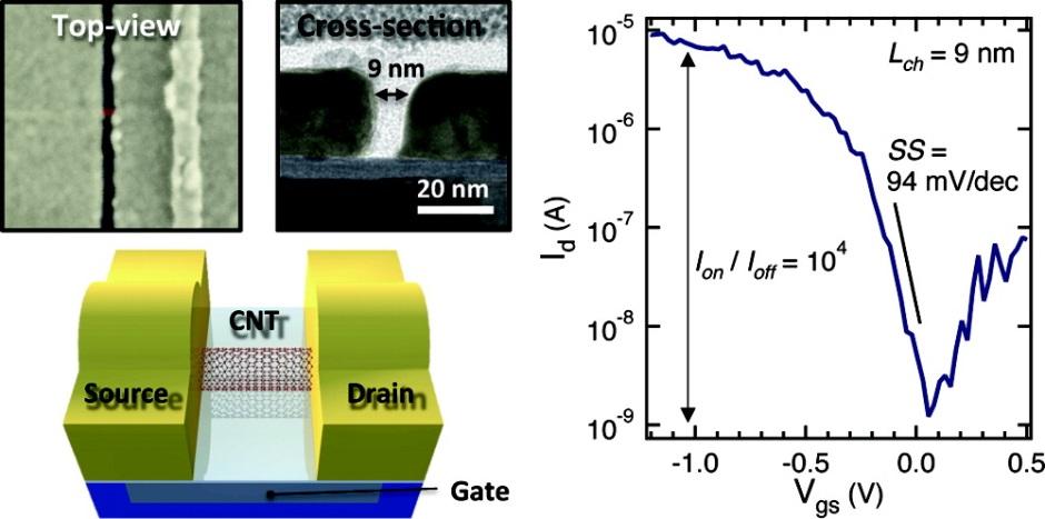
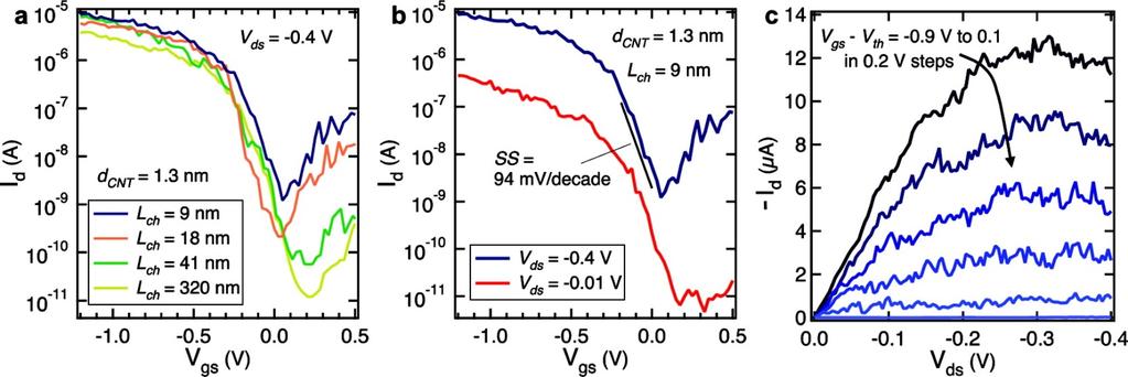
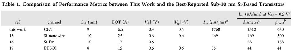
37 9 nm CNT transistor 2012 (5 nm) (20 nm) 37


38 Monolithic 3D CNT Circuits! Hai, et al., IEDM (2010) [Stanford, Mitra/Wong groups] 38

39 Graphene Forms of graphene Graphene resistivity Geim and Novoselov, Nat. Mat. (2007) [Manchester] 39

 [UCB,")
40 Bandgap Prediction for Graphene Nanoribbons Son, et al., PRL (2006) [UCB, Louie group] 40

41 Bandgap Measurements of Etched GNRs Han, et al., PRL (2007) [Columbia, Kim group] 41


42 GNR formation by unzipping CNTs Jiao, Nat. Nano. (2010) [Stanford, Dai group] 42
43 GNR Bandgap vs. width I on /I off W (nm) E g (ev) All sub-10nm GNRs are semiconducting Ion currents few ua 10 I on /Ioff exp( Eg / k 0. 8 E g ev W nm W (nm) Li, et al. Science (2008) [Dai group] 40 B T ) 50 43

44 Bottom-up Synthesized GNRs Atomically perfect edges! 7 C atoms wide W = 0.74 nm! Cai et al. Nature (2010) [EMPA (Switzerland), Fasel group] 44


45 Aligned Growth Bandstructure Measured ~2 nm pitch! m* = 0.21 m e Eg = 2.3 ev Ruffieux, et al. ACS Nano (2012) [Fasel group] 45

46 Synthesized GNR Transferred to SiO2 Bennett, et al., unpublished [UCB, Bokor/Crommie/Fischer groups] 46


47 Synthesized GNR Transistor Results Bennett, et al., unpublished [UCB, Bokor/Crommie/Fischer groups] 47

 [UCB,")
48 Wider GNRs Synthesized with 1.4 ev Gap Chen, et al., ACS Nano (2013) [UCB, Fischer/Crommie groups] 48

49 Single-Molecule Heterostructures 49

50 Summary/Outlook CNT and GNR both promising candidates for CMOS channel material for 8 nm gate length Why? High drive at low V Good scalability 3D layer stacking: 10 layers = 3 nodes on roadmap! More work needed: Purified chirality for tubes Longer, wider GNRs Dense aligned arrays Low resistance contacts GSR opportunities in my group 50
Electronics with 2D Crystals: Scaling extender, or harbinger of new functions?
 Electronics with 2D Crystals: Scaling extender, or harbinger of new functions? 1 st Workshop on Data Abundant Systems Technology Stanford, April 2014 Debdeep Jena (djena@nd.edu) Electrical Engineering,
EECS130 Integrated Circuit Devices
 EECS130 Integrated Circuit Devices Professor Ali Javey 10/30/2007 MOSFETs Lecture 4 Reading: Chapter 17, 19 Announcements The next HW set is due on Thursday. Midterm 2 is next week!!!! Threshold and Subthreshold
Supplementary Figure S1. AFM images of GraNRs grown with standard growth process. Each of these pictures show GraNRs prepared independently,
 Supplementary Figure S1. AFM images of GraNRs grown with standard growth process. Each of these pictures show GraNRs prepared independently, suggesting that the results is reproducible. Supplementary Figure
Graphene and Carbon Nanotubes
 Graphene and Carbon Nanotubes 1 atom thick films of graphite atomic chicken wire Novoselov et al - Science 306, 666 (004) 100μm Geim s group at Manchester Novoselov et al - Nature 438, 197 (005) Kim-Stormer
A Numerical Study of Scaling Issues for Schottky Barrier Carbon Nanotube Transistors
 A Numerical Study of Scaling Issues for Schottky Barrier Carbon Nanotube Transistors Jing Guo, Supriyo Datta and Mark Lundstrom School of Electrical and Computer Engineering, Purdue University, West Lafayette,
Manufacture of Nanostructures for Power Electronics Applications
 Manufacture of Nanostructures for Power Electronics Applications Brian Hunt and Jon Lai Etamota Corporation 2672 E. Walnut St. Pasadena, CA 91107 APEC, Palm Springs Feb. 23rd, 2010 1 Background Outline
OMEN an atomistic and full-band quantum transport simulator for post-cmos nanodevices
 Purdue University Purdue e-pubs Other Nanotechnology Publications Birck Nanotechnology Center 8-18-28 OMEN an atomistic and full-band quantum transport simulator for post-cmos nanodevices Mathieu Luisier
Graphene Nanoribbons: A Route to Atomically Precise Nanoelectronics Mike Crommie
 Graphene Nanoribbons: A Route to Atomically Precise Nanoelectronics Mike Crommie Dept. of Physics, UC Berkeley and Materials Science Division, LBNL Berkeley, CA Outline 1) Graphene Graphene Nanoribbon
Understanding the effect of n-type and p-type doping in the channel of graphene nanoribbon transistor
 Bull. Mater. Sci., Vol. 39, No. 5, September 2016, pp. 1303 1309. DOI 10.1007/s12034-016-1277-9 c Indian Academy of Sciences. Understanding the effect of n-type and p-type doping in the channel of graphene
Projected Performance Advantage of Multilayer Graphene Nanoribbon as Transistor Channel Material
 Projected Performance Advantage of Multilayer Graphene Nanoribbon as Transistor Channel Material Yijian Ouyang 1, Hongjie Dai 2, and Jing Guo 1 1 Department of Electrical and Computer Engineering, University
Supplementary Materials for
 advances.sciencemag.org/cgi/content/full/2/9/e1601240/dc1 Supplementary Materials for Quasi-ballistic carbon nanotube array transistors with current density exceeding Si and GaAs Gerald J. Brady, Austin
Device Performance Analysis of Graphene Nanoribbon Field-Effect Transistor with Rare- Earth Oxide (La 2 O 3 ) Based High-k Gate Dielectric
 Based High-k Gate Dielectric") Device Performance Analysis of Graphene Nanoribbon Field-Effect Transistor with Rare- Earth Oxide (La 2 O 3 ) Based High-k Gate Dielectric M. K. Bera 1, S. P. Pandey 2, A. K. Sharma 3, D. K. Tyagi 4, R.
Device Performance Analysis of Graphene Nanoribbon Field-Effect Transistor with Rare- Earth Oxide (La 2 O 3 ) Based High-k Gate Dielectric M. K. Bera 1, S. P. Pandey 2, A. K. Sharma 3, D. K. Tyagi 4, R.
Projected Performance Advantage of Multilayer Graphene Nanoribbons as a Transistor Channel Material
 1Nano Res (2010) 3: 8 15 DOI 10.1007/s12274-010-1002-8 Research Article Projected Performance Advantage of Multilayer Graphene Nanoribbons as a Transistor Channel Material Yijian Ouyang 1 ( ), Hongjie
Carbon Nanotubes in Interconnect Applications
 Carbon Nanotubes in Interconnect Applications Page 1 What are Carbon Nanotubes? What are they good for? Why are we interested in them? - Interconnects of the future? Comparison of electrical properties
Carbon Nanotube Electronics
 Carbon Nanotube Electronics Jeorg Appenzeller, Phaedon Avouris, Vincent Derycke, Stefan Heinz, Richard Martel, Marko Radosavljevic, Jerry Tersoff, Shalom Wind H.-S. Philip Wong hspwong@us.ibm.com IBM T.J.
1. Nanotechnology & nanomaterials -- Functional nanomaterials enabled by nanotechnologies.
 Novel Nano-Engineered Semiconductors for Possible Photon Sources and Detectors NAI-CHANG YEH Department of Physics, California Institute of Technology 1. Nanotechnology & nanomaterials -- Functional nanomaterials
Electric Field-Dependent Charge-Carrier Velocity in Semiconducting Carbon. Nanotubes. Yung-Fu Chen and M. S. Fuhrer
 Electric Field-Dependent Charge-Carrier Velocity in Semiconducting Carbon Nanotubes Yung-Fu Chen and M. S. Fuhrer Department of Physics and Center for Superconductivity Research, University of Maryland,
Simple Theory of the Ballistic Nanotransistor
 Simple Theory of the Ballistic Nanotransistor Mark Lundstrom Purdue University Network for Computational Nanoechnology outline I) Traditional MOS theory II) A bottom-up approach III) The ballistic nanotransistor
Towards Atomistic Simulations of the Electro-Thermal Properties of Nanowire Transistors Mathieu Luisier and Reto Rhyner
 Towards Atomistic Simulations of the Electro-Thermal Properties of Nanowire Transistors Mathieu Luisier and Reto Rhyner Integrated Systems Laboratory ETH Zurich, Switzerland Outline Motivation Electron
Evaluation of Electronic Characteristics of Double Gate Graphene Nanoribbon Field Effect Transistor for Wide Range of Temperatures
 Evaluation of Electronic Characteristics of Double Gate Graphene Nanoribbon Field Effect Transistor for Wide Range of Temperatures 1 Milad Abtin, 2 Ali Naderi 1 Department of electrical engineering, Masjed
Performance Analysis of Ultra-Scaled InAs HEMTs
 Purdue University Purdue e-pubs Birck and NCN Publications Birck Nanotechnology Center 2009 Performance Analysis of Ultra-Scaled InAs HEMTs Neerav Kharche Birck Nanotechnology Center and Purdue University,
Electro-Thermal Transport in Silicon and Carbon Nanotube Devices E. Pop, D. Mann, J. Rowlette, K. Goodson and H. Dai
 Electro-Thermal Transport in Silicon and Carbon Nanotube Devices E. Pop, D. Mann, J. Rowlette, K. Goodson and H. Dai E. Pop, 1,2 D. Mann, 1 J. Rowlette, 2 K. Goodson 2 and H. Dai 1 Dept. of 1 Chemistry
Recap (so far) Low-Dimensional & Boundary Effects
 Low-Dimensional & Boundary Effects") Recap (so far) Ohm s & Fourier s Laws Mobility & Thermal Conductivity Heat Capacity Wiedemann-Franz Relationship Size Effects and Breakdown of Classical Laws 1 Low-Dimensional & Boundary Effects Energy
Recap (so far) Ohm s & Fourier s Laws Mobility & Thermal Conductivity Heat Capacity Wiedemann-Franz Relationship Size Effects and Breakdown of Classical Laws 1 Low-Dimensional & Boundary Effects Energy
Beyond Si: Opportunities and Challenges for CMOS Technology Based on High-Mobility Channel Materials T.P. Ma Yale University
 Beyond Si: Opportunities and Challenges for CMOS Technology Based on High-Mobility Channel Materials T.P. Ma Yale University Acknowledgments: Abigail Lubow, Xiao Sun, Shufeng Ren Switching Speed of CMOS
SUPPLEMENTARY INFORMATION
 SUPPLEMENTARY INFORMATION Facile Synthesis of High Quality Graphene Nanoribbons Liying Jiao, Xinran Wang, Georgi Diankov, Hailiang Wang & Hongjie Dai* Supplementary Information 1. Photograph of graphene
EE410 vs. Advanced CMOS Structures
 EE410 vs. Advanced CMOS Structures Prof. Krishna S Department of Electrical Engineering S 1 EE410 CMOS Structure P + poly-si N + poly-si Al/Si alloy LPCVD PSG P + P + N + N + PMOS N-substrate NMOS P-well
NiCl2 Solution concentration. Etching Duration. Aspect ratio. Experiment Atmosphere Temperature. Length(µm) Width (nm) Ar:H2=9:1, 150Pa
 Width (nm) Ar:H2=9:1, 150Pa") Experiment Atmosphere Temperature #1 # 2 # 3 # 4 # 5 # 6 # 7 # 8 # 9 # 10 Ar:H2=9:1, 150Pa Ar:H2=9:1, 150Pa Ar:H2=9:1, 150Pa Ar:H2=9:1, 150Pa Ar:H2=9:1, 150Pa Ar:H2=9:1, 150Pa Ar:H2=9:1, 150Pa Ar:H2=9:1,
Experiment Atmosphere Temperature #1 # 2 # 3 # 4 # 5 # 6 # 7 # 8 # 9 # 10 Ar:H2=9:1, 150Pa Ar:H2=9:1, 150Pa Ar:H2=9:1, 150Pa Ar:H2=9:1, 150Pa Ar:H2=9:1, 150Pa Ar:H2=9:1, 150Pa Ar:H2=9:1, 150Pa Ar:H2=9:1,
Ultralow-Power Reconfigurable Computing with Complementary Nano-Electromechanical Carbon Nanotube Switches
 Ultralow-Power Reconfigurable Computing with Complementary Nano-Electromechanical Carbon Nanotube Switches Presenter: Tulika Mitra Swarup Bhunia, Massood Tabib-Azar, and Daniel Saab Electrical Eng. And
A final review session will be offered on Thursday, May 10 from 10AM to 12noon in 521 Cory (the Hogan Room).
.") A final review session will be offered on Thursday, May 10 from 10AM to 12noon in 521 Cory (the Hogan Room). The Final Exam will take place from 12:30PM to 3:30PM on Saturday May 12 in 60 Evans.» All of
A final review session will be offered on Thursday, May 10 from 10AM to 12noon in 521 Cory (the Hogan Room). The Final Exam will take place from 12:30PM to 3:30PM on Saturday May 12 in 60 Evans.» All of
Computational Model of Edge Effects in Graphene Nanoribbon Transistors
 Nano Res (2008) 1: 395 402 DOI 10.1007/s12274-008-8039-y Research Article 00395 Computational Model of Edge Effects in Graphene Nanoribbon Transistors Pei Zhao 1, Mihir Choudhury 2, Kartik Mohanram 2,
Multiple Gate CMOS and Beyond
 Multiple CMOS and Beyond Dept. of EECS, KAIST Yang-Kyu Choi Outline 1. Ultimate Scaling of MOSFETs - 3nm Nanowire FET - 8nm Non-Volatile Memory Device 2. Multiple Functions of MOSFETs 3. Summary 2 CMOS
Carbon based Nanoscale Electronics
 Carbon based Nanoscale Electronics 09 02 200802 2008 ME class Outline driving force for the carbon nanomaterial electronic properties of fullerene exploration of electronic carbon nanotube gold rush of
Carbon Nanotubes for Interconnect Applications Franz Kreupl, Andrew P. Graham, Maik Liebau, Georg S. Duesberg, Robert Seidel, Eugen Unger
 Carbon Nanotubes for Interconnect Applications Franz Kreupl, Andrew P. Graham, Maik Liebau, Georg S. Duesberg, Robert Seidel, Eugen Unger Infineon Technologies Corporate Research Munich, Germany Outline
The Critical Role of Quantum Capacitance in Compact Modeling of Nano-Scaled and Nanoelectronic Devices
 The Critical Role of Quantum Capacitance in Compact Modeling of Nano-Scaled and Nanoelectronic Devices Zhiping Yu and Jinyu Zhang Institute of Microelectronics Tsinghua University, Beijing, China yuzhip@tsinghua.edu.cn
Electrostatics of Nanowire Transistors
 Electrostatics of Nanowire Transistors Jing Guo, Jing Wang, Eric Polizzi, Supriyo Datta and Mark Lundstrom School of Electrical and Computer Engineering Purdue University, West Lafayette, IN, 47907 ABSTRACTS
Dissipative Transport in Rough Edge Graphene Nanoribbon. Tunnel Transistors
 Dissipative Transport in Rough Edge Graphene Nanoribbon Tunnel Transistors Youngki Yoon and Sayeef Salahuddin Department of Electrical Engineering and Computer Sciences, University of California, Berkeley,
Achieving a higher performance in bilayer graphene FET Strain Engineering
 SISPAD 2015, September 9-11, 2015, Washington, DC, USA Achieving a higher performance in bilayer graphene FET Strain Engineering Fan W. Chen, Hesameddin Ilatikhameneh, Gerhard Klimeck and Rajib Rahman
High Mobility Materials and Novel Device Structures for High Performance Nanoscale MOSFETs
 High Mobility Materials and Novel Device Structures for High Performance Nanoscale MOSFETs Prof. (Dr.) Tejas Krishnamohan Department of Electrical Engineering Stanford University, CA & Intel Corporation
Graphene Devices, Interconnect and Circuits Challenges and Opportunities
 Graphene Devices, Interconnect and Circuits Challenges and Opportunities Mircea R. Stan, Dincer Unluer, Avik Ghosh, Frank Tseng Univ. of Virginia, ECE Dept., Charlottesville, VA 22904 {mircea,du7x,ag7rq,ft8e}@virginia.edu
Carbon Nanotube Synaptic Transistor Network for. Pattern Recognition. Supporting Information for
 Supporting Information for Carbon Nanotube Synaptic Transistor Network for Pattern Recognition Sungho Kim 1, Jinsu Yoon 2, Hee-Dong Kim 1 & Sung-Jin Choi 2,* 1 Department of Electrical Engineering, Sejong
Metallic: 2n 1. +n 2. =3q Armchair structure always metallic = 2
 Properties of CNT d = 2.46 n 2 2 1 + n1n2 + n2 2π Metallic: 2n 1 +n 2 =3q Armchair structure always metallic a) Graphite Valence(π) and Conduction(π*) states touch at six points(fermi points) Carbon Nanotube:
Electrical Transport Properties and Field-Effect Transistors of Carbon Nanotubes
 NANO: Brief Reports and Reviews Vol. 1, No. 1 (2006) 1 4 World Scientific Publishing Company Electrical Transport Properties and Field-Effect Transistors of Carbon Nanotubes Hongjie Dai*, Ali Javey, Eric
Wafer-scale fabrication of graphene
 Wafer-scale fabrication of graphene Sten Vollebregt, MSc Delft University of Technology, Delft Institute of Mircosystems and Nanotechnology Delft University of Technology Challenge the future Delft University
Lecture 6: 2D FET Electrostatics
 Lecture 6: 2D FET Electrostatics 2016-02-01 Lecture 6, High Speed Devices 2014 1 Lecture 6: III-V FET DC I - MESFETs Reading Guide: Liu: 323-337 (he mainly focuses on the single heterostructure FET) Jena:
L ECE 4211 UConn F. Jain Scaling Laws for NanoFETs Chapter 10 Logic Gate Scaling
 L13 04202017 ECE 4211 UConn F. Jain Scaling Laws for NanoFETs Chapter 10 Logic Gate Scaling Scaling laws: Generalized scaling (GS) p. 610 Design steps p.613 Nanotransistor issues (page 626) Degradation
III-V CMOS: What have we learned from HEMTs? J. A. del Alamo, D.-H. Kim 1, T.-W. Kim, D. Jin, and D. A. Antoniadis
 III-V CMOS: What have we learned from HEMTs? J. A. del Alamo, D.-H. Kim 1, T.-W. Kim, D. Jin, and D. A. Antoniadis Microsystems Technology Laboratories, MIT 1 presently with Teledyne Scientific 23rd International
ᣂቇⴚ㗔 䇸䉮䊮䊏䊠䊷䊁䉞䉪䉴䈮䉋䉎 䊂䉱䉟䊮䋺ⶄว 㑐䈫㕖ᐔⴧ䉻䉟䊅䊚䉪䉴䇹 ᐔᚑ22ᐕᐲ ળ䇮2011ᐕ3 4ᣣ䇮 ੩ᄢቇᧄㇹ䉨䊞䊮䊌䉴 㗄 A02 ኒᐲ 㑐ᢙᴺℂ 䈮ၮ䈨䈒㕖ᐔⴧ 䊅䊉䉴䉬䊷䊦㔚 વዉ䉻䉟䊅䊚䉪䉴 ઍ ᄢᎿ ㆺ
 22201134 A02 GCOE Si device (further downsizing) Novel nanostructures (such as atomic chain) Nanoscale multi-terminal resistance measurement Carbon nanotube transistor Atomic switch Interplay:l Dynamics:
Unique Characteristics of Vertical Carbon Nanotube Field-effect Transistors on Silicon
 www.nmletters.org Unique Characteristics of Vertical Carbon Nanotube Field-effect Transistors on Silicon Jingqi Li 1,, Weisheng Yue 1, Zaibing Guo 1, Yang Yang 1, Xianbin Wang 1, Ahad A. Syed 1, Yafei
Doping-Free Fabrication of Carbon Nanotube Based Ballistic CMOS Devices and Circuits
 Doping-Free Fabrication of Carbon Nanotube Based Ballistic CMOS Devices and Circuits NANO LETTERS 2007 Vol. 7, No. 12 3603-3607 Zhiyong Zhang, Xuelei Liang,*, Sheng Wang, Kun Yao, Youfan Hu, Yuzhen Zhu,
Available online at ScienceDirect. Procedia Materials Science 11 (2015 )
") Available online at www.sciencedirect.com ScienceDirect Procedia Materials Science 11 (2015 ) 287 292 5th International Biennial Conference on Ultrafine Grained and Nanostructured Materials, UFGNSM15 Tunneling
Available online at www.sciencedirect.com ScienceDirect Procedia Materials Science 11 (2015 ) 287 292 5th International Biennial Conference on Ultrafine Grained and Nanostructured Materials, UFGNSM15 Tunneling
Performance Comparison of Graphene Nanoribbon FETs. with Schottky Contacts and Doped Reservoirs
 Performance Comparison of Graphene Nanoribbon FETs with Schottky Contacts and Doped Reservoirs Youngki Yoon 1,a, Gianluca Fiori 2,b, Seokmin Hong 1, Giuseppe Iannaccone 2, and Jing Guo 1 1 Department of
Scaling Issues in Planar FET: Dual Gate FET and FinFETs
 Scaling Issues in Planar FET: Dual Gate FET and FinFETs Lecture 12 Dr. Amr Bayoumi Fall 2014 Advanced Devices (EC760) Arab Academy for Science and Technology - Cairo 1 Outline Scaling Issues for Planar
Nanocarbon Technology for Development of Innovative Devices
 Nanocarbon Technology for Development of Innovative Devices Shintaro Sato Daiyu Kondo Shinichi Hirose Junichi Yamaguchi Graphene, a one-atom-thick honeycomb lattice made of carbon, and a carbon nanotube,
Quantum Mechanical Simulation for Ultra-thin High-k Gate Dielectrics Metal Oxide Semiconductor Field Effect Transistors
 Mechanical Simulation for Ultra-thin High-k Gate Dielectrics Metal Oxide Semiconductor Field Effect Transistors Shih-Ching Lo 1, Yiming Li 2,3, and Jyun-Hwei Tsai 1 1 National Center for High-Performance
Sub-5 nm Patterning and Applications by Nanoimprint Lithography and Helium Ion Beam Lithography
 Sub-5 nm Patterning and Applications by Nanoimprint Lithography and Helium Ion Beam Lithography Yuanrui Li 1, Ahmed Abbas 1, Yuhan Yao 1, Yifei Wang 1, Wen-Di Li 2, Chongwu Zhou 1 and Wei Wu 1* 1 Department
Journal of Electron Devices, Vol. 18, 2013, pp JED [ISSN: ]
![Journal of Electron Devices, Vol. 18, 2013, pp JED [ISSN: ]](/thumbs/86/93990983.jpg "Journal of Electron Devices, Vol. 18, 2013, pp JED [ISSN: ]") DrainCurrent-Id in linearscale(a/um) Id in logscale Journal of Electron Devices, Vol. 18, 2013, pp. 1582-1586 JED [ISSN: 1682-3427 ] SUITABILITY OF HIGH-k GATE DIELECTRICS ON THE DEVICE PERFORMANCE AND
DrainCurrent-Id in linearscale(a/um) Id in logscale Journal of Electron Devices, Vol. 18, 2013, pp. 1582-1586 JED [ISSN: 1682-3427 ] SUITABILITY OF HIGH-k GATE DIELECTRICS ON THE DEVICE PERFORMANCE AND
GHZ ELECTRICAL PROPERTIES OF CARBON NANOTUBES ON SILICON DIOXIDE MICRO BRIDGES
 GHZ ELECTRICAL PROPERTIES OF CARBON NANOTUBES ON SILICON DIOXIDE MICRO BRIDGES SHENG F. YEN 1, HAROON LAIS 1, ZHEN YU 1, SHENGDONG LI 1, WILLIAM C. TANG 1,2, AND PETER J. BURKE 1,2 1 Electrical Engineering
MSE 310/ECE 340: Electrical Properties of Materials Fall 2014 Department of Materials Science and Engineering Boise State University
 MSE 310/ECE 340: Electrical Properties of Materials Fall 2014 Department of Materials Science and Engineering Boise State University Practice Final Exam 1 Read the questions carefully Label all figures
Tunneling characteristics of graphene
 Tunneling characteristics of graphene Young Jun Shin, 1,2 Gopinadhan Kalon, 1,2 Jaesung Son, 1 Jae Hyun Kwon, 1,2 Jing Niu, 1 Charanjit S. Bhatia, 1 Gengchiau Liang, 1 and Hyunsoo Yang 1,2,a) 1 Department
3D Simulation of coaxial carbon nanotube field effect transistor
 3D Simulation of coaxial carbon nanotube field effect transistor Dinh Sy Hien, Nguyen Thi Luong, Thi Tran Anh Tuan and Dinh Viet Nga HCM University of Natural Sciences, 7 Nguyen Van Cu Street, 5 District,
CHAPTER 5 EFFECT OF GATE ELECTRODE WORK FUNCTION VARIATION ON DC AND AC PARAMETERS IN CONVENTIONAL AND JUNCTIONLESS FINFETS
 98 CHAPTER 5 EFFECT OF GATE ELECTRODE WORK FUNCTION VARIATION ON DC AND AC PARAMETERS IN CONVENTIONAL AND JUNCTIONLESS FINFETS In this chapter, the effect of gate electrode work function variation on DC
IEEE TRANSACTIONS ON ELECTRON DEVICES 1. Quantum Modeling and Proposed Designs of CNT-Embedded Nanoscale MOSFETs
 TRANSACTIONS ON ELECTRON DEVICES 1 Quantum Modeling and Proposed Designs of CNT-Embedded Nanoscale MOSFETs Akin Akturk, Gary Pennington, and Neil Goldsman Abstract We propose a novel MOSFET design that
Emerging Interconnect Technologies for CMOS and beyond-cmos Circuits
 Emerging Interconnect Technologies for CMOS and beyond-cmos Circuits Sou-Chi Chang, Rouhollah M. Iraei Vachan Kumar, Ahmet Ceyhan and Azad Naeemi School of Electrical & Computer Engineering Georgia Institute
Application of High-κ Gate Dielectrics and Metal Gate Electrodes to enable Silicon and Non-Silicon Logic Nanotechnology
 Application of High-κ Gate Dielectrics and Metal Gate Electrodes to enable Silicon and Non-Silicon Logic Nanotechnology Robert Chau, Justin Brask, Suman Datta, Gilbert Dewey, Mark Doczy, Brian Doyle, Jack
Power and Heat: The Big Picture
 Power Power Density (W/cm 2 ) Power Dissipation in Nanoscale CMOS and Carbon Nanotubes Eric Pop Dept. of Electrical & Computer Engineering http://poplab.ece.uiuc.edu E. Pop 1 Power and Heat: The Big Picture
CMOS Scaling. Two motivations to scale down. Faster transistors, both digital and analog. To pack more functionality per area. Lower the cost!
 Two motivations to scale down CMOS Scaling Faster transistors, both digital and analog To pack more functionality per area. Lower the cost! (which makes (some) physical sense) Scale all dimensions and
Growth of Aligned SWNTs in Quartz Substrates. Jie Liu Department of Chemistry Duke University April 10, 2011 Guadalupe Workshop
 Growth of Aligned SWNTs in Quartz Substrates Jie Liu Department of Chemistry Duke University April 10, 2011 Guadalupe Workshop Carbon Nanotube Structure θ = tan 1 [ 3m /( m + 2n)] d = 2 ac c 3( n + nm
FLCC Seminar. Spacer Lithography for Reduced Variability in MOSFET Performance
 1 Seminar Spacer Lithography for Reduced Variability in MOSFET Performance Prof. Tsu-Jae King Liu Electrical Engineering & Computer Sciences Dept. University of California at Berkeley Graduate Student:
3-month progress Report
 3-month progress Report Graphene Devices and Circuits Supervisor Dr. P.A Childs Table of Content Abstract... 1 1. Introduction... 1 1.1 Graphene gold rush... 1 1.2 Properties of graphene... 3 1.3 Semiconductor
SUPPLEMENTARY INFORMATION
 SUPPLEMENTARY INFORMATION DOI: 10.1038/NNANO.2011.138 Graphene Nanoribbons with Smooth Edges as Quantum Wires Xinran Wang, Yijian Ouyang, Liying Jiao, Hailiang Wang, Liming Xie, Justin Wu, Jing Guo, and
Frequency dispersion effect and parameters. extraction method for novel HfO 2 as gate dielectric
 048 SCIENCE CHINA Information Sciences April 2010 Vol. 53 No. 4: 878 884 doi: 10.1007/s11432-010-0079-8 Frequency dispersion effect and parameters extraction method for novel HfO 2 as gate dielectric LIU
A Multi-Gate CMOS Compact Model BSIMMG
 A Multi-Gate CMOS Compact Model BSIMMG Darsen Lu, Sriramkumar Venugopalan, Tanvir Morshed, Yogesh Singh Chauhan, Chung-Hsun Lin, Mohan Dunga, Ali Niknejad and Chenming Hu University of California, Berkeley
Electrical Contacts to Carbon Nanotubes Down to 1nm in Diameter
 1 Electrical Contacts to Carbon Nanotubes Down to 1nm in Diameter Woong Kim, Ali Javey, Ryan Tu, Jien Cao, Qian Wang, and Hongjie Dai* Department of Chemistry and Laboratory for Advanced Materials, Stanford
What are Carbon Nanotubes? What are they good for? Why are we interested in them?
 Growth and Properties of Multiwalled Carbon Nanotubes What are Carbon Nanotubes? What are they good for? Why are we interested in them? - Interconnects of the future? - our vision Where do we stand - our
The World of Carbon Nanotubes
 The World of Carbon Nanotubes Carbon Nanotubes Presentation by Jan Felix Eschermann at JASS05 from March 31st to April 9th, 2005 1 Outline Introduction Physical Properties Manufacturing Techniques Applications
Prospects for Ge MOSFETs
 Prospects for Ge MOSFETs Sematech Workshop December 4, 2005 Dimitri A. Antoniadis Microsystems Technology Laboratories MIT Sematech Workshop 2005 1 Channel Transport - I D I D =WQ i (x 0 )v xo v xo : carrier
ALD high-k and higher-k integration on GaAs
 ALD high-k and higher-k integration on GaAs Ozhan Koybasi 1), Min Xu 1), Yiqun Liu 2), Jun-Jieh Wang 2), Roy G. Gordon 2), and Peide D. Ye 1)* 1) School of Electrical and Computer Engineering, Purdue University,
This is the author s final accepted version.
 Al-Ameri, T., Georgiev, V.P., Adamu-Lema, F. and Asenov, A. (2017) Does a Nanowire Transistor Follow the Golden Ratio? A 2D Poisson- Schrödinger/3D Monte Carlo Simulation Study. In: 2017 International
There's Plenty of Room at the Bottom
 There's Plenty of Room at the Bottom 12/29/1959 Feynman asked why not put the entire Encyclopedia Britannica (24 volumes) on a pin head (requires atomic scale recording). He proposed to use electron microscope
Research Opportunities in Macroelectronics. Motivation, Application Overview. Materials Classes, Challenges. Patterning Techniques, Challenges
 Research Opportunities in Macroelectronics Motivation, Application Overview Materials Classes, Challenges Patterning Techniques, Challenges John A. Rogers -- University of Illinois at Urbana/Champaign
Diameter Optimization for Highest Degree of Ballisticity of Carbon Nanotube Field Effect Transistors I. Khan, O. Morshed and S. M.
 Diameter Optimization for Highest Degree of Ballisticity of Carbon Nanotube Field Effect Transistors I. Khan, O. Morshed and S. M. Mominuzzaman Department of Electrical and Electronic Engineering, Bangladesh
MOS Transistors. Prof. Krishna Saraswat. Department of Electrical Engineering Stanford University Stanford, CA
 MOS Transistors Prof. Krishna Saraswat Department of Electrical Engineering S Stanford, CA 94305 saraswat@stanford.edu 1 1930: Patent on the Field-Effect Transistor! Julius Lilienfeld filed a patent describing
High-Performance Carbon Nanotube Transistors on SrTiO 3 /Si. Substrates
 1 High-Performance Carbon Nanotube Transistors on SrTiO 3 /Si Substrates B. M. Kim a),b), T. Brintlinger a), E. Cobas a), Haimei Zheng c), and M. S. Fuhrer a),d) University of Maryland, College Park, Maryland
Drift-diffusion model for single layer transition metal dichalcogenide field-effect transistors
 Drift-diffusion model for single layer transition metal dichalcogenide field-effect transistors David Jiménez Departament d'enginyeria Electrònica, Escola d'enginyeria, Universitat Autònoma de Barcelona,
Carbon Nanotubes (CNTs)
") Carbon Nanotubes (s) Seminar: Quantendynamik in mesoskopischen Systemen Florian Figge Fakultät für Physik Albert-Ludwigs-Universität Freiburg July 7th, 2010 F. Figge (University of Freiburg) Carbon Nanotubes
Carbon Nanotubes (s) Seminar: Quantendynamik in mesoskopischen Systemen Florian Figge Fakultät für Physik Albert-Ludwigs-Universität Freiburg July 7th, 2010 F. Figge (University of Freiburg) Carbon Nanotubes
Hydrogenation of Single Walled Carbon Nanotubes
 Hydrogenation of Single Walled Carbon Nanotubes Anders Nilsson Stanford Synchrotron Radiation Laboratory (SSRL) and Stockholm University Coworkers and Ackowledgement A. Nikitin 1), H. Ogasawara 1), D.
Modeling of Carbon Nanotube Field Effect Transistors
 8 Modeling of Carbon Nanotube Field Effect Transistors Dinh Sy Hien HCM City University of Natural Sciences, Vietnam 1. Introduction Since the discovery of carbon nanotubes (CNTs) by Iijima in 1991 [1],
SUPPLEMENTARY INFORMATION
 High-density integration of carbon nanotubes by chemical self-assembly Hongsik Park, Ali Afzali, Shu-Jen Han, George S. Tulevski, Aaron D. Franklin, Jerry Tersoff, James B. Hannon and Wilfried Haensch
Graphene Novel Material for Nanoelectronics
 Graphene Novel Material for Nanoelectronics Shintaro Sato Naoki Harada Daiyu Kondo Mari Ohfuchi (Manuscript received May 12, 2009) Graphene is a flat monolayer of carbon atoms with a two-dimensional honeycomb
Electronic and Photonic Applications of One- Dimensional Carbon and Silicon Nanostructures
 Electronic and Photonic Applications of One- Dimensional Carbon and Silicon Nanostructures Anupama B. Kaul Jet Propulsion Laboratory, California Institute of Technology, Pasadena, CA 91109 Ph: (818) 393-7186;
NANOELECTRONICS beyond CMOS
 NANOELECTRONICS beyond CMOS David Pulfrey 1 NNI definition of Nanotechnology 1-10 nm is better But Intel prefer... 2 Bourianoff04 1 3 Bourianoff04 4 Moravec04 2 Increasing the Integration Level functional
SECTION: Circle one: Alam Lundstrom. ECE 305 Exam 5 SOLUTIONS: Spring 2016 April 18, 2016 M. A. Alam and M.S. Lundstrom Purdue University
 NAME: PUID: SECTION: Circle one: Alam Lundstrom ECE 305 Exam 5 SOLUTIONS: April 18, 2016 M A Alam and MS Lundstrom Purdue University This is a closed book exam You may use a calculator and the formula
Carbon Nanomaterials: Nanotubes and Nanobuds and Graphene towards new products 2030
 Carbon Nanomaterials: Nanotubes and Nanobuds and Graphene towards new products 2030 Prof. Dr. Esko I. Kauppinen Helsinki University of Technology (TKK) Espoo, Finland Forecast Seminar February 13, 2009
Short-Channel Field Effect Transistors with 9-Atom. and 13-Atom wide Graphene Nanoribbons
 Short-Channel Field Effect Transistors with 9-Atom and 13-Atom wide Graphene Nanoribbons Juan Pablo Llinas 1, Andrew Fairbrother 2, Gabriela Barin 2, Pascal Ruffieux 2, Wu Shi 4, Kyunghoon Lee 1, Byung
Ultra-Scaled InAs HEMTs
 Performance Analysis of Ultra-Scaled InAs HEMTs Neerav Kharche 1, Gerhard Klimeck 1, Dae-Hyun Kim 2,3, Jesús. A. del Alamo 2, and Mathieu Luisier 1 1 Network for Computational ti Nanotechnology and Birck
Directions for simulation of beyond-cmos devices. Dmitri Nikonov, George Bourianoff, Mark Stettler
 Directions for simulation of beyond-cmos devices Dmitri Nikonov, George Bourianoff, Mark Stettler Outline Challenges and responses in nanoelectronic simulation Limits for electronic devices and motivation
PROGRESS AND ISSUES IN DIELECTRIC MATERIALS FOR SUB-100NM DRAM TECHNOLOGY ABSTRACT
 PROGRESS AND ISSUES IN DIELECTRIC MATERIALS FOR SUB-100NM DRAM TECHNOLOGY Kanta Saino Device Integration Group, Technology & Development Office, Elpida Memory Inc. 7-10 Yoshikawakogyodanchi, Higashihiroshima,
Non-equilibrium Green's function (NEGF) simulation of metallic carbon nanotubes including vacancy defects
 simulation of metallic carbon nanotubes including vacancy defects") Purdue University Purdue e-pubs Other Nanotechnology Publications Birck Nanotechnology Center 6-1-2007 Non-equilibrium Green's function (NEGF) simulation of metallic carbon nanotubes including vacancy
Purdue University Purdue e-pubs Other Nanotechnology Publications Birck Nanotechnology Center 6-1-2007 Non-equilibrium Green's function (NEGF) simulation of metallic carbon nanotubes including vacancy
Design Of Ternary Logic Gates Using CNTFET
 International Journal of Research in Computer and Communication Technology, Vol 4, Issue 3, March -2015 ISSN (Online) 2278-5841 ISSN (Print) 2320-5156 Design Of Ternary Logic Gates Using CNTFET Aashish
GRAPHENE NANORIBBONS Nahid Shayesteh,
 USC Department of Physics Graduate Seminar 1 GRAPHENE NANORIBBONS Nahid Shayesteh, Outlines 2 Carbon based material Discovery and innovation of graphen Graphene nanoribbons structure Application of Graphene