Graphene Nanoribbons: A Route to Atomically Precise Nanoelectronics Mike Crommie
|
|
|
- Derrick Wood
- 6 years ago
- Views:
Transcription


1 Graphene Nanoribbons: A Route to Atomically Precise Nanoelectronics Mike Crommie Dept. of Physics, UC Berkeley and Materials Science Division, LBNL Berkeley, CA
 New developments in bottom-up fabrication Molecular bandgap engineering New bottom-up strategies Graphene")
2 Outline 1) Graphene Graphene Nanoribbon (GNR) behavior 2) Potential applications for GNRs. 3) How do we make GNRs? 4) New developments in bottom-up fabrication Molecular bandgap engineering New bottom-up strategies Graphene Nanoribbon


3 Electronic Structure of Graphene K Energy Conduction band Valence band Dirac pt. zigzag direction k y k x M armchair direction Reciprocal Space k x K k y M
4 Graphene Nanoribbon Electronic Structure w Armchair Reciprocal Space Armchair E 0 No Edge State (ev) k 0 Zigzag Reciprocal Space Zigzag E 0 Edge State (ev) Spin-polarized k 0 M. Fujita, et al., J. Phys. Soc. Jpn 65, 1920 (1996); K. Nakada, et al., PRB 54, (1996); J. Heyd et al, J. Chem. Phys. 118, 8207 (2003); Y.-W. Son, et al, PRL 97, (2006)

5 Potential GNR Device Advantages Energy gap, capacitance Bandgap Engineering GNRs solve the nanotube metallicity problem V SD Big gap Small gap Width E V G I D V G for nanotubes k µ Energy Length off Smaller capacitance H. Park, et al., Nat. Nanotech. 7, 787 (2012) Faster on Uniquely Efficient Tunneling GNR GNR Fast onset tube tube Length
6 Potential GNR Device Advantages Energy gap, capacitance Bandgap Engineering GNRs solve the nanotube metallicity problem V SD Big gap Small gap Width E V G I D V G for nanotubes k µ Energy off Smaller capacitance H. Park, et al., Nat. Nanotech. 7, 787 (2012) Faster on Uniquely Efficient Tunneling GNR GNR Fast onset tube tube Length


7 High-current low-dissipation switching: HFET New proposed GNR implementation Requires GNR doping and bandgap/width variation Large gap Small gap Large gap S p n D J. Bokor

 Y.")
 Ritter and")
8 How Do We Make High Quality GNR Devices? Top-down Lithography M. Y. Han et al., PRL 98, (2007) Rough Edges are a Problem Graphene platelet on Si(100) Y. Kobayash et al., PRB 71, (2005) Ritter and Lyding, Nat. Mat. 8, 235 (2009)
 GNR width = 20 nm 5.")
 Kosynkin, et al,")


9 Unzipping Nanotubes: A Better Edge Unzipped GNRs Smooth Edges (8, 1) GNR width = 20 nm 5.5 Å Jiao, et al, Nat. Nanotechnol 5, 321 (2010) Kosynkin, et al, Nature 458, 872 (2009) Au(111) 48 Å 48 Å 0.0 Å C. Tao, et al., Nat. Phys. 7, 616 (2011) Unzipped GNR FETs High Mobility Controlling width and chirality A problem X. Wang, et al, Nat. Nanotechnol 6, 563 (2011)
10 A New Idea Molecular precursor Bottom-up Fabrication: Final assembled GNR
11 A New Idea Molecular precursor Bottom-up Fabrication: Final assembled GNR Width Chirality Edge functionalization Bottom-up Heterostructures: p n p p-n junctions bandgap engineering


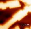
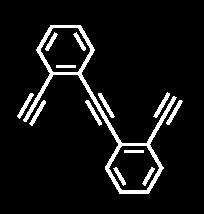
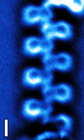
12 GNR Bottom-up Synthesis Breakthrough: n=7 AGNRs Precursor molecule Metallic surfaces. 200 C n = 7 AGNR. 200 C 400 C (7 atoms across) STM Image: AGNRs / Au(111) Width = 0.7 nm Fasel, Muellen, & co-workers J. Cai et al, Nature 466, 470 (2010)


13 STM Allows Measurement of Local Electronic Structure STM Spectroscopy tip sample V tip sample E F Ñwω E F LDOS(E) 0

 P. Ruffieux, et al.")
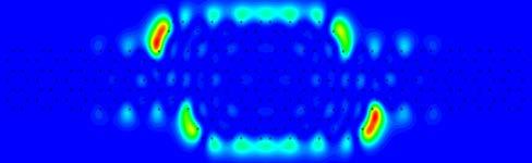
14 Using STM to Measure GNR Energy Gap GNR Electronic Structure STM Bandedge Electrons Show Higher Density at GNR Edges GNR = 2.5 ev Au reference LUMO di/dv map M. Koch, et al., Nat. Nanotech. 7, 713 (2012) P. Ruffieux, et al., ACS Nano 6, 6930 (2012)

15 Can We Tune the Energy Gap? (ev) Armchair 4 N=7 Tune? 2? 0 N = 7 N > 7 Must synthesize new precursor molecules


16 A New Precursor Molecule to Tune GNR Bandgap: N=13 New Precursor 200 C. 200 C 400 C n = 13 Metallic surface. F. Fischer & Crommie STM image: Polymer stage Fully cyclized (after annealing) width = 1.4 nm Yen-Chia Chen, et al., ACS Nano 7, 6123 (2013)

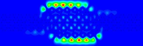
17 STM Spectroscopy of N=13 AGNR GNR width width N = 13 = N = 7 2 Au N = 13 = N = di/dv maps HOMO LUMO Y.-C. Chen et al., ACS Nano 7, 6123 (2013)
 GaAs AlGaAs GaAs 5-9 Junction E E c E v x Sevinçli, et al, PRB 78, 245402 (2008)")
18 Variable-Width Heterostructures + Molecular Bandgap Engineering (B.E.) Previous Mesoscale B.E. : New Molecule-scale B.E. : (theory, DFT) GaAs AlGaAs GaAs 5-9 Junction E E c E v x Sevinçli, et al, PRB 78, (2008)
19 Molecular Bandgap Engineering: 7-13 Junctions n=7 n= Junction


20 Molecular Bandgap Engineering: 7-13 Junctions n=7 n= Junction Fabricating 7-13 Molecular Junctions on Au(111) 3.8 nm 2 nm

21 STM Spectroscopy of 7-13 Junction Topograph N=7 N=13
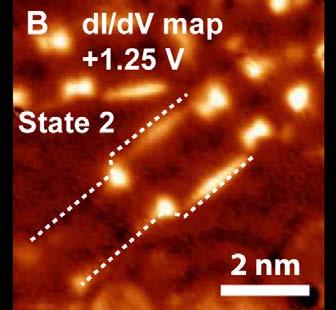
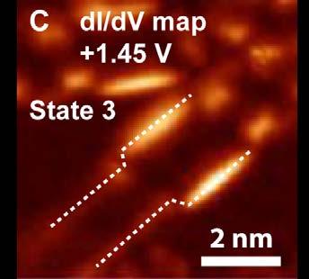
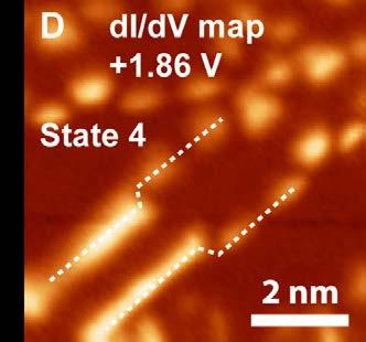
22 STM Spectroscopy of 7-13 Junction: Interface States Topograph N=7 N=13 1 2

23 STM Spectroscopy of 7-13 Junction: Interface States Topograph N=7 N=13 1 2
24 Theoretically Modeling the 7-13 Molecular Junction Assume Periodic Structure: Perform DFT Calculation Unit Cell Theory: Ting Cao, Steven Louie
25 Electronic Structure of 7-13 Molecular Junction n=13 LUMO n = ev n = ev D.O.S Energy (ev) -1.0 Calculate LDOS distribution for these states, compare to experiment S. G. Louie, T. Cao


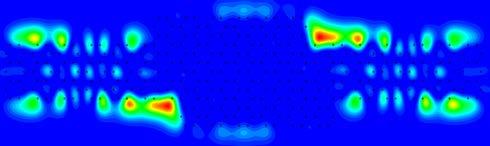
26 Topograph Comparing Theoretical Wave-function Maps to Experiment Experimental LDOS Theoretical LDOS


27 How Can Devices be Made From Bottom-up GNRs? A Must transfer GNRs to insulator: SiO 2 PMMA Au Mica GNRs Mica Device Layout for 7-AGNRs 26nm gap Fischer, Crommie, Bokor

28 Bottom-up GNR Device Results Bottom-up N=7 GNR FET Schottky barrier behavior: E k µ n-type Φ e E metal contact GNR metal contact x Challenges: Improve contacts Improve transfer to insulator New GNR heterostructures Grow directly on insulator? P. B. Bennett et al., APL 103, (2013)
 SiO 2 Difficult Bergman Cyclization of Enediynes: Flexible")
 A. Riss, et al., Nano Lett.")
29 New Chemistry: New Opportunities Currently requires metal substrate Au(111) SiO 2 Difficult Bergman Cyclization of Enediynes: Flexible coupling: + Alkyne coupling.. Radical step growth Polymerization:..Q. Sun, et al., JACS 135, 8448 (2013) A. Riss, et al., Nano Lett. 14, 2251 (2014)


30 Model System for Surface Chemistry Enediyne Fragment: Felix Fischer (UC Berkeley) Expected Reaction Path: But what really happens?
31 Imaging Enediyene Cyclization on Ag(100) STM Images heat
 L.")
 tip Qplus nc-afm G.")
32 Imaging Enediyene Cyclization on Ag(100) STM Images heat F. J. Giessibl, Appl. Phys. Lett. 76, 1470 (2000) L. Gross, F. Mohn, N. Moll, P. Liljeroth, G. Meyer, Science 325, 1110 (2009) tip Qplus nc-afm G. Meyer & co-workers (2009)

 STM")


33 Imaging Enediyene Cyclization on Ag(100) STM Images heat nc-afm Images D. Oteyza, et al., Science, /science (2013)

34 Modifying Enediyne Molecules to Induce Coupling Alkyne Coupling heat Enediynes on Ag(100)


35 Modifying Enediyne Molecules to Induce Coupling Radical Polymerization heat Enediynes on Au(111)
36 Energy Landscape and Reaction Pathway Theory: A. Rubio & co-workers D. de Oteyza, et al., Science 340, 1434 (2013)
37 Energy Landscape and Reaction Pathway Theory: A. Rubio & co-workers Improved Structural Control at the Nanoscale D. de Oteyza, et al., Science 340, 1434 (2013)
38 Conclusions 1) GNRs novel electronic properties. 2) Bottom-up synthesis molecular bandgap engineering. 3) New chemistries new nanostructures. Future 1) Incorporate bottom-up heterojunctions into devices. 2) New bottom-up GNR structures, improved control. 3) Grow GNRs directly on insulators.
 Dimas G.de Oteyza (now at Centro de Fisica, San Seb.")
 Steven Louie (Physics) Sebastian Wickenberg Jeff Bokor (EECS) Hsinzon Tsai Marvin Cohen (Physics) Patrick Bennett Alex Zettl (Physics)")
39 Collaborators / Funding Nano-Bio Spect. Gp., ETSF Sci. Dev. Center, UPV, San Sebastian, Spain: Angel Rubio, Duncan J. Mowbray, Alejandro Perez UC Berkeley / LBL: M. F. Crommie (Physics) Dimas G.de Oteyza (now at Centro de Fisica, San Seb., Spain) Felix Fischer (Chemistry) Alexander Riss (now at Inst. of App. Phys., TU Wien) Steven Louie (Physics) Sebastian Wickenberg Jeff Bokor (EECS) Hsinzon Tsai Marvin Cohen (Physics) Patrick Bennett Alex Zettl (Physics) Miguel Moreno-Ugeda Zahra Pedramrazi Chen Chen Aaron Bradley Danny Haberer Grisha Etkin Patrick Gorman Liang Z. Tan Ivan Pechenezhskiy Yenchia Chen
40 THE END
Short-Channel Field Effect Transistors with 9-Atom. and 13-Atom wide Graphene Nanoribbons
 Short-Channel Field Effect Transistors with 9-Atom and 13-Atom wide Graphene Nanoribbons Juan Pablo Llinas 1, Andrew Fairbrother 2, Gabriela Barin 2, Pascal Ruffieux 2, Wu Shi 4, Kyunghoon Lee 1, Byung
Abstract Keywords INTRODUCTION
 Experimental confirmation of the existence of the three-electron bond and theoretical basis of its existence. Bezverkhniy Volodymyr Dmytrovych e - mail: bezvold@ukr.net Ukraine Abstract: Analysis of images
Carbon-Based Electronics: Will there be a carbon age to follow the silicon age? Jeffrey Bokor EECS Department UC Berkeley
 Carbon-Based Electronics: Will there be a carbon age to follow the silicon age? Jeffrey Bokor EECS Department UC Berkeley jbokor@eecs.berkeley.edu Solid State Seminar 9-13-13 1 Outline Review of development
Bottom-up Graphene Nanoribbon Field-Effect. Transistors.
 Bottom-up Graphene Nanoribbon Field-Effect Transistors. Patrick B. Bennett 1,2, Zahra Pedramrazi 3, Ali Madani 2, Yen-Chia Chen 3,6, Dimas G. de Oteyza 3,5, Chen Chen 4, Felix R. Fischer 4,6, Michael F.
Outline. Introduction: graphene. Adsorption on graphene: - Chemisorption - Physisorption. Summary
 Outline Introduction: graphene Adsorption on graphene: - Chemisorption - Physisorption Summary 1 Electronic band structure: Electronic properties K Γ M v F = 10 6 ms -1 = c/300 massless Dirac particles!
Supplementary Information for Solution-Synthesized Chevron Graphene Nanoribbons Exfoliated onto H:Si(100)
") Supplementary Information for Solution-Synthesized Chevron Graphene Nanoribbons Exfoliated onto H:Si(100) Adrian Radocea,, Tao Sun,, Timothy H. Vo, Alexander Sinitskii,,# Narayana R. Aluru,, and Joseph
Supplementary Information for Solution-Synthesized Chevron Graphene Nanoribbons Exfoliated onto H:Si(100) Adrian Radocea,, Tao Sun,, Timothy H. Vo, Alexander Sinitskii,,# Narayana R. Aluru,, and Joseph
9AGNR Local Back-gate Graphene Nanoribbon Short-field Transistors
 9AGNR Local Back-gate Graphene Nanoribbon Short-field Transistors Robert Lear Electrical Engineering and Computer Sciences University of California at Berkeley Technical Report No. UCB/EECS-2017-86 http://www2.eecs.berkeley.edu/pubs/techrpts/2017/eecs-2017-86.html
Branislav K. Nikolić
 First-principles quantum transport modeling of thermoelectricity in nanowires and single-molecule nanojunctions Branislav K. Nikolić Department of Physics and Astronomy, University of Delaware, Newark,
Sulfur-doped graphene nanoribbons with a sequence of distinct band gaps
 Nano Research 2017, 10(10): 3377 3384 DOI 10.1007/s12274-017-1550-2 Sulfur-doped graphene nanoribbons with a sequence of distinct band gaps Yan-Fang Zhang 1,5,, Yi Zhang 1,, Geng Li 1, Jianchen Lu 1, Yande
Light Emission from Ultranarrow Graphene Nanoribbons Edge and Termini Effects. Deborah Prezzi CNR Nanoscience Institute, Modena, Italy
 Light Emission from Ultranarrow Graphene Nanoribbons Edge and Termini Effects Deborah Prezzi CNR Nanoscience Institute, Modena, Italy Graphene Nanostructures Quantum Confinement Open a band gap by confining
Supplementary Figure S1. AFM images of GraNRs grown with standard growth process. Each of these pictures show GraNRs prepared independently,
 Supplementary Figure S1. AFM images of GraNRs grown with standard growth process. Each of these pictures show GraNRs prepared independently, suggesting that the results is reproducible. Supplementary Figure
Interatomic bonding 1
 Interatomic bonding 1 Bonding forces of atoms All forces playing role in bonding are electrostatic Coulomb forces. Nuclei attract electrons, but nuclei repulse each other as well as electrons do. So, bonding
Supporting Information. Nanoscale control of rewriteable doping patterns in pristine graphene/boron nitride heterostructures
 Supporting Information Nanoscale control of rewriteable doping patterns in pristine graphene/boron nitride heterostructures Jairo Velasco Jr. 1,5,, Long Ju 1,, Dillon Wong 1,, Salman Kahn 1, Juwon Lee
Surface Transfer Doping of Diamond by Organic Molecules
 Surface Transfer Doping of Diamond by Organic Molecules Qi Dongchen Department of Physics National University of Singapore Supervisor: Prof. Andrew T. S. Wee Dr. Gao Xingyu Scope of presentation Overview
Understanding the effect of n-type and p-type doping in the channel of graphene nanoribbon transistor
 Bull. Mater. Sci., Vol. 39, No. 5, September 2016, pp. 1303 1309. DOI 10.1007/s12034-016-1277-9 c Indian Academy of Sciences. Understanding the effect of n-type and p-type doping in the channel of graphene
Wang Shiyong ( 王世勇 ) Supervisor: Prof. Lin Nian. Department of Physics, The Hong Kong University of Science and Technology, Clear Water Bay, Hong Kong
 Supervisor: Prof. Lin Nian. Department of Physics, The Hong Kong University of Science and Technology, Clear Water Bay, Hong Kong") Characterization of electronic structures of single molecules, conjugated polymers and molecular nanostructures using low temperature scanning tunneling microscopy Wang Shiyong ( 王世勇 ) Supervisor: Prof.
Characterization of electronic structures of single molecules, conjugated polymers and molecular nanostructures using low temperature scanning tunneling microscopy Wang Shiyong ( 王世勇 ) Supervisor: Prof.
1. Nanotechnology & nanomaterials -- Functional nanomaterials enabled by nanotechnologies.
 Novel Nano-Engineered Semiconductors for Possible Photon Sources and Detectors NAI-CHANG YEH Department of Physics, California Institute of Technology 1. Nanotechnology & nanomaterials -- Functional nanomaterials
Local Electronic and Chemical Structure of Oligo-acetylene Derivatives Formed Through Radical Cyclizations at a Surface
 pubs.acs.org/nanolett Terms of Use CC-BY Downloaded via 148.251.232.83 on August 18, 2018 at 11:30:36 (UTC). See https://pubs.acs.org/sharingguidelines for options on how to legitimately share published
tunneling theory of few interacting atoms in a trap
 tunneling theory of few interacting atoms in a trap Massimo Rontani CNR-NANO Research Center S3, Modena, Italy www.nano.cnr.it Pino D Amico, Andrea Secchi, Elisa Molinari G. Maruccio, M. Janson, C. Meyer,
ELECTRONIC ENERGY DISPERSION AND STRUCTURAL PROPERTIES ON GRAPHENE AND CARBON NANOTUBES
 ELECTRONIC ENERGY DISPERSION AND STRUCTURAL PROPERTIES ON GRAPHENE AND CARBON NANOTUBES D. RACOLTA, C. ANDRONACHE, D. TODORAN, R. TODORAN Technical University of Cluj Napoca, North University Center of
Projected Performance Advantage of Multilayer Graphene Nanoribbons as a Transistor Channel Material
 1Nano Res (2010) 3: 8 15 DOI 10.1007/s12274-010-1002-8 Research Article Projected Performance Advantage of Multilayer Graphene Nanoribbons as a Transistor Channel Material Yijian Ouyang 1 ( ), Hongjie
GRAPHENE NANORIBBONS Nahid Shayesteh,
 USC Department of Physics Graduate Seminar 1 GRAPHENE NANORIBBONS Nahid Shayesteh, Outlines 2 Carbon based material Discovery and innovation of graphen Graphene nanoribbons structure Application of Graphene
Spin and Charge transport in Ferromagnetic Graphene
 Spin and Charge transport in Ferromagnetic Graphene Hosein Cheraghchi School of Physics, Damghan University Recent Progress in D Systems, Oct, 4, IPM Outline: Graphene Spintronics Background on graphene
MSE 310/ECE 340: Electrical Properties of Materials Fall 2014 Department of Materials Science and Engineering Boise State University
 MSE 310/ECE 340: Electrical Properties of Materials Fall 2014 Department of Materials Science and Engineering Boise State University Practice Final Exam 1 Read the questions carefully Label all figures
SUPPLEMENTARY INFORMATION
 SUPPLEMENTARY INFORMATION Facile Synthesis of High Quality Graphene Nanoribbons Liying Jiao, Xinran Wang, Georgi Diankov, Hailiang Wang & Hongjie Dai* Supplementary Information 1. Photograph of graphene
Electron transport through molecular junctions and FHI-aims
 STM m metallic surface Electron transport through molecular junctions and FHI-aims Alexei Bagrets Inst. of Nanotechnology (INT) & Steinbuch Centre for Computing (SCC) @ Karlsruhe Institute of Technology
Lecture 6: 2D FET Electrostatics
 Lecture 6: 2D FET Electrostatics 2016-02-01 Lecture 6, High Speed Devices 2014 1 Lecture 6: III-V FET DC I - MESFETs Reading Guide: Liu: 323-337 (he mainly focuses on the single heterostructure FET) Jena:
Supplementary Figure 1. Electron micrographs of graphene and converted h-bn. (a) Low magnification STEM-ADF images of the graphene sample before
 Low magnification STEM-ADF images of the graphene sample before") Supplementary Figure 1. Electron micrographs of graphene and converted h-bn. (a) Low magnification STEM-ADF images of the graphene sample before conversion. Most of the graphene sample was folded after
Supplementary Figure 1. Electron micrographs of graphene and converted h-bn. (a) Low magnification STEM-ADF images of the graphene sample before conversion. Most of the graphene sample was folded after
Transversal electric field effect in multilayer graphene nanoribbon
 Transversal electric field effect in multilayer graphene nanoribbon S. Bala kumar and Jing Guo a) Department of Electrical and Computer Engineering, University of Florida, Gainesville, Florida 32608, USA
ᣂቇⴚ㗔 䇸䉮䊮䊏䊠䊷䊁䉞䉪䉴䈮䉋䉎 䊂䉱䉟䊮䋺ⶄว 㑐䈫㕖ᐔⴧ䉻䉟䊅䊚䉪䉴䇹 ᐔᚑ22ᐕᐲ ળ䇮2011ᐕ3 4ᣣ䇮 ੩ᄢቇᧄㇹ䉨䊞䊮䊌䉴 㗄 A02 ኒᐲ 㑐ᢙᴺℂ 䈮ၮ䈨䈒㕖ᐔⴧ 䊅䊉䉴䉬䊷䊦㔚 વዉ䉻䉟䊅䊚䉪䉴 ઍ ᄢᎿ ㆺ
 22201134 A02 GCOE Si device (further downsizing) Novel nanostructures (such as atomic chain) Nanoscale multi-terminal resistance measurement Carbon nanotube transistor Atomic switch Interplay:l Dynamics:
Supporting Information
 Supporting Information Monolithically Integrated Flexible Black Phosphorus Complementary Inverter Circuits Yuanda Liu, and Kah-Wee Ang* Department of Electrical and Computer Engineering National University
Device Performance Analysis of Graphene Nanoribbon Field-Effect Transistor with Rare- Earth Oxide (La 2 O 3 ) Based High-k Gate Dielectric
 Based High-k Gate Dielectric") Device Performance Analysis of Graphene Nanoribbon Field-Effect Transistor with Rare- Earth Oxide (La 2 O 3 ) Based High-k Gate Dielectric M. K. Bera 1, S. P. Pandey 2, A. K. Sharma 3, D. K. Tyagi 4, R.
Device Performance Analysis of Graphene Nanoribbon Field-Effect Transistor with Rare- Earth Oxide (La 2 O 3 ) Based High-k Gate Dielectric M. K. Bera 1, S. P. Pandey 2, A. K. Sharma 3, D. K. Tyagi 4, R.
Electronic Properties of Hydrogenated Quasi-Free-Standing Graphene
 GCOE Symposium Tohoku University 2011 Electronic Properties of Hydrogenated Quasi-Free-Standing Graphene Danny Haberer Leibniz Institute for Solid State and Materials Research Dresden Co-workers Supervising
The experimental work seems to be well carried out and the DFT calculations carefully crafted.
 Reviewers' comments: Reviewer #1 (Remarks to the Author): The manuscript by Maier et al. reports on the on-surface synthesis of 1D and 2D polymers in ultra-high vacuum. A halogenated triphenylamine precursor
Scanning Tunneling Microscopy
 Scanning Tunneling Microscopy Scanning Direction References: Classical Tunneling Quantum Mechanics Tunneling current Tunneling current I t I t (V/d)exp(-Aφ 1/2 d) A = 1.025 (ev) -1/2 Å -1 I t = 10 pa~10na
Black phosphorus: A new bandgap tuning knob
 Black phosphorus: A new bandgap tuning knob Rafael Roldán and Andres Castellanos-Gomez Modern electronics rely on devices whose functionality can be adjusted by the end-user with an external knob. A new
Edge chirality determination of graphene by Raman spectroscopy
 Edge chirality determination of graphene by Raman spectroscopy YuMeng You, ZhenHua Ni, Ting Yu, ZeXiang Shen a) Division of Physics and Applied Physics, School of Physical and Mathematical Sciences, Nanyang
From manipulation of the charge state to imaging of individual molecular orbitals and bond formation
 Scanning Probe Microscopy of Adsorbates on Insulating Films: From manipulation of the charge state to imaging of individual molecular orbitals and bond formation Gerhard Meyer, Jascha Repp, Peter Liljeroth
Surface atoms/molecules of a material act as an interface to its surrounding environment;
 1 Chapter 1 Thesis Overview Surface atoms/molecules of a material act as an interface to its surrounding environment; their properties are often complicated by external adsorbates/species on the surface
Theoretical Modeling of Tunneling Barriers in Carbon-based Molecular Electronic Junctions
 Second Revised version, jp-2014-09838e Supporting Information Theoretical Modeling of Tunneling Barriers in Carbon-based Molecular Electronic Junctions Mykola Kondratenko 1,2, Stanislav R. Stoyanov 1,3,4,
Carbon based Nanoscale Electronics
 Carbon based Nanoscale Electronics 09 02 200802 2008 ME class Outline driving force for the carbon nanomaterial electronic properties of fullerene exploration of electronic carbon nanotube gold rush of
From nanophysics research labs to cell phones. Dr. András Halbritter Department of Physics associate professor
 From nanophysics research labs to cell phones Dr. András Halbritter Department of Physics associate professor Curriculum Vitae Birth: 1976. High-school graduation: 1994. Master degree: 1999. PhD: 2003.
Projected Performance Advantage of Multilayer Graphene Nanoribbon as Transistor Channel Material
 Projected Performance Advantage of Multilayer Graphene Nanoribbon as Transistor Channel Material Yijian Ouyang 1, Hongjie Dai 2, and Jing Guo 1 1 Department of Electrical and Computer Engineering, University
arxiv: v1 [cond-mat.mes-hall] 13 Sep 2007
![arxiv: v1 [cond-mat.mes-hall] 13 Sep 2007](/thumbs/80/81765575.jpg "arxiv: v1 [cond-mat.mes-hall] 13 Sep 2007") Graphene Nanoribbon and Graphene Nanodisk Motohiko Ezawa Department of Physics, University of Tokyo, arxiv:0709.2066v1 [cond-mat.mes-hall] 13 Sep 2007 Hongo 7-3-1, Tokyo 113-0033, Japan Abstract We study
Graphene Nanoribbon and Graphene Nanodisk Motohiko Ezawa Department of Physics, University of Tokyo, arxiv:0709.2066v1 [cond-mat.mes-hall] 13 Sep 2007 Hongo 7-3-1, Tokyo 113-0033, Japan Abstract We study
Spatially resolving density-dependent screening around a single charged atom in graphene
 Supplementary Information for Spatially resolving density-dependent screening around a single charged atom in graphene Dillon Wong, Fabiano Corsetti, Yang Wang, Victor W. Brar, Hsin-Zon Tsai, Qiong Wu,
SCIENCE & TECHNOLOGY
 Pertanika J. Sci. & Technol. 25 (S): 205-212 (2017) SCIENCE & TECHNOLOGY Journal homepage: http://www.pertanika.upm.edu.my/ Effect of Boron and Oxygen Doping to Graphene Band Structure Siti Fazlina bt
Transport through Andreev Bound States in a Superconductor-Quantum Dot-Graphene System
 Transport through Andreev Bound States in a Superconductor-Quantum Dot-Graphene System Nadya Mason Travis Dirk, Yung-Fu Chen, Cesar Chialvo Taylor Hughes, Siddhartha Lal, Bruno Uchoa Paul Goldbart University
Graphene Devices, Interconnect and Circuits Challenges and Opportunities
 Graphene Devices, Interconnect and Circuits Challenges and Opportunities Mircea R. Stan, Dincer Unluer, Avik Ghosh, Frank Tseng Univ. of Virginia, ECE Dept., Charlottesville, VA 22904 {mircea,du7x,ag7rq,ft8e}@virginia.edu
& Dirac Fermion confinement Zahra Khatibi
 Graphene & Dirac Fermion confinement Zahra Khatibi 1 Outline: What is so special about Graphene? applications What is Graphene? Structure Transport properties Dirac fermions confinement Necessity External
Scanning Tunneling Microscopy (STM)
") Page 1 of 8 Scanning Tunneling Microscopy (STM) This is the fastest growing surface analytical technique, which is replacing LEED as the surface imaging tool (certainly in UHV, air and liquid). STM has
Page 1 of 8 Scanning Tunneling Microscopy (STM) This is the fastest growing surface analytical technique, which is replacing LEED as the surface imaging tool (certainly in UHV, air and liquid). STM has
Hydrogenated Graphene
 Hydrogenated Graphene Stefan Heun NEST, Istituto Nanoscienze-CNR and Scuola Normale Superiore Pisa, Italy Outline Epitaxial Graphene Hydrogen Chemisorbed on Graphene Hydrogen-Intercalated Graphene Outline
Dissipative Transport in Rough Edge Graphene Nanoribbon. Tunnel Transistors
 Dissipative Transport in Rough Edge Graphene Nanoribbon Tunnel Transistors Youngki Yoon and Sayeef Salahuddin Department of Electrical Engineering and Computer Sciences, University of California, Berkeley,
(a) (b) Supplementary Figure 1. (a) (b) (a) Supplementary Figure 2. (a) (b) (c) (d) (e)
 (b) Supplementary Figure 1. (a) (b) (a) Supplementary Figure 2. (a) (b) (c) (d) (e)") (a) (b) Supplementary Figure 1. (a) An AFM image of the device after the formation of the contact electrodes and the top gate dielectric Al 2 O 3. (b) A line scan performed along the white dashed line
(a) (b) Supplementary Figure 1. (a) An AFM image of the device after the formation of the contact electrodes and the top gate dielectric Al 2 O 3. (b) A line scan performed along the white dashed line
CVD growth of Graphene. SPE ACCE presentation Carter Kittrell James M. Tour group September 9 to 11, 2014
 CVD growth of Graphene SPE ACCE presentation Carter Kittrell James M. Tour group September 9 to 11, 2014 Graphene zigzag armchair History 1500: Pencil-Is it made of lead? 1789: Graphite 1987: The first
Graphene: the Route from Touch Screens to Digital Nanoelectronics
 Graphene: the Route from Touch Screens to Digital Nanoelectronics László Péter Biró Research Institute for Technical Physics & Materials Science, Budapest, Hungary http://www.nanotechnology.hu/ Human History
en électronique moléculaire
 Al Au Au hydrogen carbon oxygen sulfur silicon SiO2 1nm SiO2 1nm SiO2 1nm Si highly doped Si highly doped Si highly doped -(CH2)3-SH or C3-SH -(CH2)3-CH3 or C3 -(CH2)6-CH=CH2 or C8 1.0µm Quelques avancées
Supporting Information for Ultra-narrow metallic armchair graphene nanoribbons
 Supporting Information for Ultra-narrow metallic armchair graphene nanoribbons Supplementary Figure 1 Ribbon length statistics. Distribution of the ribbon lengths and the fraction of kinked ribbons for
Physics and Material Science of Semiconductor Nanostructures
 Physics and Material Science of Semiconductor Nanostructures PHYS 570P Prof. Oana Malis Email: omalis@purdue.edu Course website: http://www.physics.purdue.edu/academic_programs/courses/phys570p/ Lecture
Supporting Information: Local Electronic Structure of a Single-Layer. Porphyrin-Containing Covalent Organic Framework
 Supporting Information: Local Electronic Structure of a Single-Layer Porphyrin-Containing Covalent Organic Framework Chen Chen 1, Trinity Joshi 2, Huifang Li 3, Anton D. Chavez 4,5, Zahra Pedramrazi 2,
(Co-PIs-Mark Brongersma, Yi Cui, Shanhui Fan) Stanford University. GCEP Research Symposium 2013 Stanford, CA October 9, 2013
 Stanford University. GCEP Research Symposium 2013 Stanford, CA October 9, 2013") High-efficiency thin film nano-structured multi-junction solar James S. cells Harris (PI) (Co-PIs-Mark Brongersma, Yi Cui, Shanhui Fan) Stanford University GCEP Research Symposium 2013 Stanford, CA October
High-efficiency thin film nano-structured multi-junction solar James S. cells Harris (PI) (Co-PIs-Mark Brongersma, Yi Cui, Shanhui Fan) Stanford University GCEP Research Symposium 2013 Stanford, CA October
2) Atom manipulation. Xe / Ni(110) Model: Experiment:
 Atom manipulation. Xe / Ni(110) Model: Experiment:") 2) Atom manipulation D. Eigler & E. Schweizer, Nature 344, 524 (1990) Xe / Ni(110) Model: Experiment: G.Meyer, et al. Applied Physics A 68, 125 (1999) First the tip is approached close to the adsorbate
2) Atom manipulation D. Eigler & E. Schweizer, Nature 344, 524 (1990) Xe / Ni(110) Model: Experiment: G.Meyer, et al. Applied Physics A 68, 125 (1999) First the tip is approached close to the adsorbate
Session Chair: Prof. Haiping Cheng (University of Florida) Dr. Lei Shen. National University of Singapore
 Dr. Lei Shen. National University of Singapore") B1. Modeling Quantum Transport at Nanoscale Chair(s): Chun ZHANG, National University of Singapore, Singapore Session s Title (if available) Tue - 17 Jan 2017 13:00 ~ 14:30 Room 2 Session Chair: Prof.
B1. Modeling Quantum Transport at Nanoscale Chair(s): Chun ZHANG, National University of Singapore, Singapore Session s Title (if available) Tue - 17 Jan 2017 13:00 ~ 14:30 Room 2 Session Chair: Prof.
GW and Bethe-Salpeter Equation Approach to Spectroscopic Properties. Steven G. Louie
 GW and Bethe-Salpeter Equation Approach to Spectroscopic Properties Steven G. Louie Department of Physics, University of California at Berkeley and Materials Sciences Division, Lawrence Berkeley National
QS School Summary
 2018 NSF/DOE/AFOSR Quantum Science Summer School June 22, 2018 QS 3 2018 School Summary Kyle Shen (Cornell) Some Thank yous! A Big Thanks to Caroline Brockner!!! Also to our fantastic speakers! Kavli Institute
Optimizing Graphene Morphology on SiC(0001)
") Optimizing Graphene Morphology on SiC(0001) James B. Hannon Rudolf M. Tromp Graphene sheets Graphene sheets can be formed into 0D,1D, 2D, and 3D structures Chemically inert Intrinsically high carrier mobility
Optimizing Graphene Morphology on SiC(0001) James B. Hannon Rudolf M. Tromp Graphene sheets Graphene sheets can be formed into 0D,1D, 2D, and 3D structures Chemically inert Intrinsically high carrier mobility
single-electron electron tunneling (SET)
") single-electron electron tunneling (SET) classical dots (SET islands): level spacing is NOT important; only the charging energy (=classical effect, many electrons on the island) quantum dots: : level spacing
single-electron electron tunneling (SET) classical dots (SET islands): level spacing is NOT important; only the charging energy (=classical effect, many electrons on the island) quantum dots: : level spacing
Sub-5 nm Patterning and Applications by Nanoimprint Lithography and Helium Ion Beam Lithography
 Sub-5 nm Patterning and Applications by Nanoimprint Lithography and Helium Ion Beam Lithography Yuanrui Li 1, Ahmed Abbas 1, Yuhan Yao 1, Yifei Wang 1, Wen-Di Li 2, Chongwu Zhou 1 and Wei Wu 1* 1 Department
Optical & Transport Properties of Carbon Nanotubes II
 Optical & Transport Properties of Carbon Nanotubes II Duncan J. Mowbray Nano-Bio Spectroscopy Group European Theoretical Spectroscopy Facility (ETSF) Donostia International Physics Center (DIPC) Universidad
Emerging Interconnect Technologies for CMOS and beyond-cmos Circuits
 Emerging Interconnect Technologies for CMOS and beyond-cmos Circuits Sou-Chi Chang, Rouhollah M. Iraei Vachan Kumar, Ahmet Ceyhan and Azad Naeemi School of Electrical & Computer Engineering Georgia Institute
Atomically Resolved Single-Walled Carbon Nanotube Intramolecular Junctions
 Atomically Resolved Single-Walled Carbon Nanotube Intramolecular Junctions The Harvard community has made this article openly available. Please share how this access benefits you. Your story matters Citation
Perfect spin-fillter and spin-valve in carbon atomic chains
 Perfect spin-fillter and spin-valve in carbon atomic chains M. G. Zeng,1, 2 L. Shen,1 Y. Q. Cai,1 Z. D. Sha,1 and Y. P. Feng1, * 1Department of Physics, National University of Singapore, 2 Science Drive
Computational Model of Edge Effects in Graphene Nanoribbon Transistors
 Nano Res (2008) 1: 395 402 DOI 10.1007/s12274-008-8039-y Research Article 00395 Computational Model of Edge Effects in Graphene Nanoribbon Transistors Pei Zhao 1, Mihir Choudhury 2, Kartik Mohanram 2,
Physics in two dimensions in the lab
 Physics in two dimensions in the lab Nanodevice Physics Lab David Cobden PAB 308 Collaborators at UW Oscar Vilches (Low Temperature Lab) Xiaodong Xu (Nanoscale Optoelectronics Lab) Jiun Haw Chu (Quantum
Engineering the electronic structure of atomically-precise graphene nanoribbons. Giang Duc Nguyen
 Engineering the electronic structure of atomically-precise graphene nanoribbons by Giang Duc Nguyen A dissertation submitted in partial satisfaction of the requirements for the degree of Doctor of Philosophy
Imaging Single-Molecule Reaction Intermediates Stabilized by Surface Dissipation and Entropy
 Imaging Single-Molecule Reaction Intermediates Stabilized by Surface Dissipation and Entropy Alexander Riss 1,2,,*, Alejandro Pérez Paz 3,, Sebastian Wickenburg 1,4,, Hsin-Zon Tsai 1, Dimas G. de Oteyza
Scanning Tunneling Microscopy. how does STM work? the quantum mechanical picture example of images how can we understand what we see?
 Scanning Tunneling Microscopy how does STM work? the quantum mechanical picture example of images how can we understand what we see? Observation of adatom diffusion with a field ion microscope Scanning
Synthesis of armchair graphene nanoribbons from the 10,10 -dibromo-9,9 -bianthracene molecules on Ag(111): the role of organometallic intermediates
: the role of organometallic intermediates") www.nature.com/scientificreports Received: 9 November 2017 Accepted: 1 February 2018 Published: xx xx xxxx OPEN Synthesis of armchair graphene nanoribbons from the 10,10 -dibromo-9,9 -bianthracene molecules
www.nature.com/scientificreports Received: 9 November 2017 Accepted: 1 February 2018 Published: xx xx xxxx OPEN Synthesis of armchair graphene nanoribbons from the 10,10 -dibromo-9,9 -bianthracene molecules
GRAPHENE NANORIBBONS Nahid Shayesteh,
 USC Department of Physics Graduate Seminar GRAPHENE NANORIBBONS Nahid Shayesteh, Outlines 2 Carbon based material Discovery and innovation of graphen Graphene nanoribbons structure and... FUNCTIONS 3 Carbon-based
Molecular Dynamics Study of Thermal Rectification in Graphene Nanoribbons
 Molecular Dynamics Study of Thermal Rectification in Graphene Nanoribbons Jiuning Hu 1* Xiulin Ruan 2 Yong P. Chen 3# 1School of Electrical and Computer Engineering and Birck Nanotechnology Center, Purdue
Elementary Process of Electromigration at Metallic Nanojunctions in the Ballistic Regime
 Elementary Process of Electromigration at Metallic Nanojunctions in the Ballistic Regime Kaz Hirakawa Institute of Industrial Science, University of Tokyo CREST, JST collaborators: Akinori Umeno, Kenji
Novel materials and nanostructures for advanced optoelectronics
 Novel materials and nanostructures for advanced optoelectronics Q. Zhuang, P. Carrington, M. Hayne, A Krier Physics Department, Lancaster University, UK u Brief introduction to Outline Lancaster University
NiCl2 Solution concentration. Etching Duration. Aspect ratio. Experiment Atmosphere Temperature. Length(µm) Width (nm) Ar:H2=9:1, 150Pa
 Width (nm) Ar:H2=9:1, 150Pa") Experiment Atmosphere Temperature #1 # 2 # 3 # 4 # 5 # 6 # 7 # 8 # 9 # 10 Ar:H2=9:1, 150Pa Ar:H2=9:1, 150Pa Ar:H2=9:1, 150Pa Ar:H2=9:1, 150Pa Ar:H2=9:1, 150Pa Ar:H2=9:1, 150Pa Ar:H2=9:1, 150Pa Ar:H2=9:1,
Experiment Atmosphere Temperature #1 # 2 # 3 # 4 # 5 # 6 # 7 # 8 # 9 # 10 Ar:H2=9:1, 150Pa Ar:H2=9:1, 150Pa Ar:H2=9:1, 150Pa Ar:H2=9:1, 150Pa Ar:H2=9:1, 150Pa Ar:H2=9:1, 150Pa Ar:H2=9:1, 150Pa Ar:H2=9:1,
SUPPLEMENTARY INFORMATION
 SUPPLEMENTARY INFORMATION Probing the Influence of Edge Structure on the Electronic Properties of Graphene Quantum Dots and Nanoribbons with Scanning Tunneling Microscopy Kyle A. Ritter 1,2 and Joseph
Typical example of the FET: MEtal Semiconductor FET (MESFET)
") Typical example of the FET: MEtal Semiconductor FET (MESFET) Conducting channel (RED) is made of highly doped material. The electron concentration in the channel n = the donor impurity concentration N
Typical example of the FET: MEtal Semiconductor FET (MESFET) Conducting channel (RED) is made of highly doped material. The electron concentration in the channel n = the donor impurity concentration N
Planar Organic Photovoltaic Device. Saiful I. Khondaker
 Planar Organic Photovoltaic Device Saiful I. Khondaker Nanoscience Technology Center and Department of Physics University of Central Florida http://www.physics.ucf.edu/~khondaker W Metal 1 L ch Metal 2
Energy gaps of atomically precise armchair graphene nanoribbons
 Energy gaps of atomically precise armchair graphene nanoribbons Wen-Xiao Wang 1, Mei Zhou 2, Xinqi Li 3, Si-Yu Li 1, Xiaosong Wu 3, Wenhui Duan 2, and Lin He 1, * 1 Center for Advanced Quantum Studies,
DEFECTS IN 2D MATERIALS: HOW WE TAUGHT ELECTRONIC SCREENING TO MACHINES
 DEFECTS IN 2D MATERIALS: HOW WE TAUGHT ELECTRONIC SCREENING TO MACHINES Johannes Lischner Imperial College London LISCHNER GROUP AT IMPERIAL COLLEGE LONDON Theory and simulation of materials: focus on
Self-Assembly of Two-Dimensional Organic Networks Containing Heavy Metals (Pb, Bi) and Preparation of Spin-Polarized Scanning Tunneling Microscope
 and Preparation of Spin-Polarized Scanning Tunneling Microscope") MPhil Thesis Defense Self-Assembly of Two-Dimensional Organic Networks Containing Heavy Metals (Pb, Bi) and Preparation of Spin-Polarized Scanning Tunneling Microscope Presented by CHEN Cheng 12 th Aug.
MPhil Thesis Defense Self-Assembly of Two-Dimensional Organic Networks Containing Heavy Metals (Pb, Bi) and Preparation of Spin-Polarized Scanning Tunneling Microscope Presented by CHEN Cheng 12 th Aug.
Nanoelectronics. Topics
 Nanoelectronics Topics Moore s Law Inorganic nanoelectronic devices Resonant tunneling Quantum dots Single electron transistors Motivation for molecular electronics The review article Overview of Nanoelectronic
Nanocarbon Technology for Development of Innovative Devices
 Nanocarbon Technology for Development of Innovative Devices Shintaro Sato Daiyu Kondo Shinichi Hirose Junichi Yamaguchi Graphene, a one-atom-thick honeycomb lattice made of carbon, and a carbon nanotube,
Solid State Device Fundamentals
 Solid State Device Fundamentals ENS 345 Lecture Course by Alexander M. Zaitsev alexander.zaitsev@csi.cuny.edu Tel: 718 982 2812 Office 4N101b 1 Outline - Goals of the course. What is electronic device?
Supporting Information
 Copyright WILEY-VCH Verlag GmbH & Co. KGaA, 69469 Weinheim, Germany, 2015. Supporting Information for Adv. Funct. Mater., DOI: 10.1002/adfm.201503131 Tuning the Excitonic States in MoS 2 /Graphene van
Carbon Nanomaterials
 Carbon Nanomaterials STM Image 7 nm AFM Image Fullerenes C 60 was established by mass spectrographic analysis by Kroto and Smalley in 1985 C 60 is called a buckminsterfullerene or buckyball due to resemblance
High Performance, Low Operating Voltage n-type Organic Field Effect Transistor Based on Inorganic-Organic Bilayer Dielectric System
 Journal of Physics: Conference Series PAPER OPEN ACCESS High Performance, Low Operating Voltage n-type Organic Field Effect Transistor Based on Inorganic-Organic Bilayer Dielectric System To cite this
Designing interfaces for Spin Injection into Organic Molecular Solids: A Surface Science Approach
 Designing interfaces for Spin Injection into Organic Molecular Solids: A Surface Science Approach SESAPS November 11, 2016 Jingying Wang, Drew Deloach, Dan Dougherty Department of Physics and Organic and
Herre van der Zant. interplay between molecular spin and electron transport (molecular spintronics) Gate
 Gate") transport through the single molecule magnet Mn12 Herre van der Zant H.B. Heersche, Z. de Groot (Delft) C. Romeike, M. Wegewijs (RWTH Aachen) D. Barreca, E. Tondello (Padova) L. Zobbi, A. Cornia (Modena)
transport through the single molecule magnet Mn12 Herre van der Zant H.B. Heersche, Z. de Groot (Delft) C. Romeike, M. Wegewijs (RWTH Aachen) D. Barreca, E. Tondello (Padova) L. Zobbi, A. Cornia (Modena)
Quantum Effects and Phase Tuning in Epitaxial 2H- and 1T -MoTe 2 Monolayers
 Supplementary Information Quantum Effects and Phase Tuning in Epitaxial 2H- and 1T -MoTe 2 Monolayers Jinglei Chen, Guanyong Wang,, ǁ Yanan Tang,, Hao Tian,,# Jinpeng Xu, Xianqi Dai,, Hu Xu, # Jinfeng
3-month progress Report
 3-month progress Report Graphene Devices and Circuits Supervisor Dr. P.A Childs Table of Content Abstract... 1 1. Introduction... 1 1.1 Graphene gold rush... 1 1.2 Properties of graphene... 3 1.3 Semiconductor
Electronic level alignment at metal-organic contacts with a GW approach
 Electronic level alignment at metal-organic contacts with a GW approach Jeffrey B. Neaton Molecular Foundry, Lawrence Berkeley National Laboratory Collaborators Mark S. Hybertsen, Center for Functional
Characterization of a Surface Reaction by means of Atomic Force Microscopy
 Article Subscriber access provided by KIT Library Karlsruhe Institute of Technology Characterization of a Surface Reaction by means of Atomic Force Microscopy Florian Albrecht, Niko Pavli#ek, Coral Herranz-Lancho,