& Dirac Fermion confinement Zahra Khatibi
|
|
|
- Darren Reed
- 5 years ago
- Views:
Transcription

1 Graphene & Dirac Fermion confinement Zahra Khatibi 1
2 Outline: What is so special about Graphene? applications What is Graphene? Structure Transport properties Dirac fermions confinement Necessity External magnetic field Strain engineering Pseudo magnetic fields Conclusion 2
3 What is so special about Graphene? 3


4 What is so special about Graphene? 4 Andre Geim Konstantin Novoselov K. S. Novoselov, et al., SCIENCE VOL (2004)
5 What is so special about Graphene? Graphene has the strongest material stiffness ever measured (1.0 TPa) has high thermal conductivity is chemically stable can withstand large current densities has very high mobility has ballistic transport over sub-micron scales 5 N.M.R Peres et al., J. Phys.: Condens. Matter 21 (2009)

6 What is so special about Graphene? 6


7 What is so special about Graphene? High performance transistors silicon-based electronics Quantum Von Neumann architecture in single chip graphene-based electronics Two inductors and a transistor Can be used as amplifiers and wireless communication 7


8 What is so special about Graphene? Perfect solar cells Out of 1000 watts of sunlight silicon solar cell: 14 watts graphene-based solar cell: 1.3 watts graphene-based hybrid film on a flexible plastic substrate 8


9 What is so special about Graphene? Better lenses mobile-phone cameras, webcams and auto-focusing eye glasses Spin lens 9 Veselago s lens SCIENCE VOL (2007) Computer simulation of electron charge density
10 What is graphene? 10

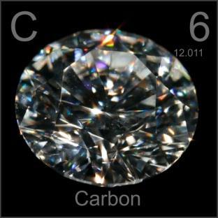
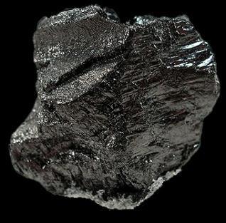
11 What is is graphene? (structure) Graphitic materials 11

12 What is graphene? (structure) 12

13 What is graphene? (structure) 13
 A honey comb")
14 What is graphene? (structure) A honey comb lattice 14
15 What is graphene? (structure) A honey comb lattice 15
16 What is is graphene? (structure) A honey comb lattice 16
17 What is graphene? (structure) A honey comb lattice Sub lattices: A B 17
 Band")


18 What is graphene? (structure) Band structure t ' : NNN hopping energy 1.42 A r 1 r 2 t 0 t =0 t: NN hopping energy 18 G. Baskaran, S. A. Jafari, Novel Quantum Phenomena in Graphene
 Dirac points Six Fermi points at six corners of BZ")
19 What is graphene? (structure) Dirac points Six Fermi points at six corners of BZ (only 2 are independent) E/t 19
 Klein tunneling 200 ev 285 ev Transparent")

20 What is graphene? (Transport properties) Klein tunneling 200 ev 285 ev Transparent barriers for some angles No backscattering Lack of localization for smooth potential over atomic scale 20 M.I.Katsnelson et al., nature physics VOL (2006) Transmission probability
21 Dirac fermions confinement 21


22 Dirac fermions confinement (necessity) Not the only but the most important reason Graphene-based field effect transistors (FET) high mobility & ballistic transport at submicron distances structures smaller than 10 nm with higher mobility graphene gapless spectrum? Flow spreading switch off 22
23 External magnetic field 23
24 External magnetic field Inhomogeneous magnetic fields no transmission is possible for 24 A. De Martino et al., PRL 98, (2007) Transmission probability T for a magnetic barrier of width 2d


25 armchair External magnetic field Zigzag states Zigzag 25 K. Wakabayashi et al., PRB (1999)

26 External magnetic field circular dot in magnetic field (10 T) ❶ ❷ ❸ ❶ ❷ ❸ independent particle Hartree bands parabolic potential Energy spectrum of a graphene quantum dot at B = 10 T 26 N.M.R Peres et al., J. Phys.: Condens. Matter (2009)
27 Strain engineering 27

 Disorder")

28 Strain engineering (pseudo magnetic field) Disorder changes hopping energy by: distance Pz orbitals angle 28

29 Strain engineering (pseudo magnetic field) Hopping energies modification Change in bond length Change in unit cell area 29


30 Strain engineering (pseudo magnetic field) Inversion symmetry φ r = φ r A = A x (r) + ia y (r) AB BB AA BA 30

31 Strain engineering (pseudo magnetic field) Time reversal is not broken C depends on detailed model of chemical bonding β and g are the coupling to acoustical wave in graphene 31 M.A.H. Vozmedianoa et al., arxiv: v2 (2010)
")


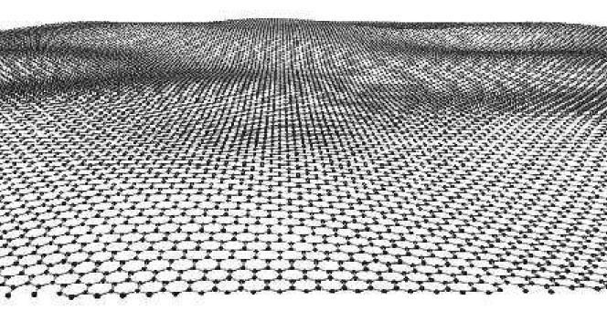
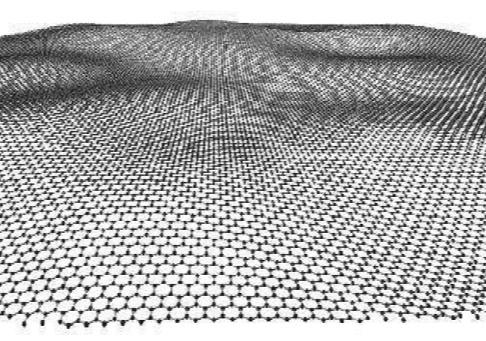
32 Strain engineering (pseudo magnetic field) strong pseudomagnetic field which guides electrons 32 N. Levy et al., SCIENCE VOL (2010)


33 Strain engineering (pseudo magnetic field) ring-shaped Gaussian deformation B ps sin 3θ Pseudo magnetic field Classical trajectories Current density 33 G. M. M. Wakker et al., PHYSICAL REVIEW B 84, (2011)
 tip or")

34 Strain engineering (pseudo magnetic field) rotationally symmetric strain Made by atomic force microscopy (AFM) tip or by a homogeneous gas pressure vertical displacement 34 K.J Kim et al., PHYSICAL REVIEW B 84, (R) (2011) Pseudo magnetic field

35 Strain engineering (pseudo magnetic field) rotationally symmetric strain Classical trajectories Probability density 35 K.J Kim et al., PHYSICAL REVIEW B 84, (R) (2011)


36 Strain engineering (pseudo magnetic field) Tunable gap in strained graphene 36 Current density T. Low et al., PHYSICAL REVIEW B 83, (2011)
37 Conclusion Graphene is a promising candidate for nano-electronic applications. Confinement is achievable via strain engineering or external fields. 37

38 Thank you 38
Graphene and Quantum Hall (2+1)D Physics
D Physics") The 4 th QMMRC-IPCMS Winter School 8 Feb 2011, ECC, Seoul, Korea Outline 2 Graphene and Quantum Hall (2+1)D Physics Lecture 1. Electronic structures of graphene and bilayer graphene Lecture 2. Electrons
The 4 th QMMRC-IPCMS Winter School 8 Feb 2011, ECC, Seoul, Korea Outline 2 Graphene and Quantum Hall (2+1)D Physics Lecture 1. Electronic structures of graphene and bilayer graphene Lecture 2. Electrons
3-month progress Report
 3-month progress Report Graphene Devices and Circuits Supervisor Dr. P.A Childs Table of Content Abstract... 1 1. Introduction... 1 1.1 Graphene gold rush... 1 1.2 Properties of graphene... 3 1.3 Semiconductor
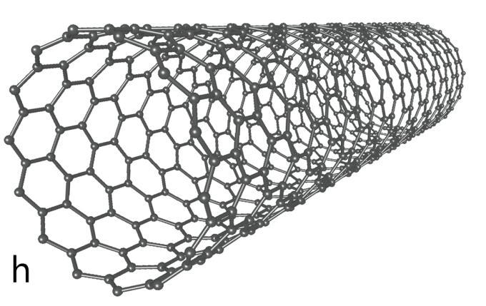
Graphene and Carbon Nanotubes
 Graphene and Carbon Nanotubes 1 atom thick films of graphite atomic chicken wire Novoselov et al - Science 306, 666 (004) 100μm Geim s group at Manchester Novoselov et al - Nature 438, 197 (005) Kim-Stormer
GRAPHENE the first 2D crystal lattice
 GRAPHENE the first 2D crystal lattice dimensionality of carbon diamond, graphite GRAPHENE realized in 2004 (Novoselov, Science 306, 2004) carbon nanotubes fullerenes, buckyballs what s so special about
Quantum transport through graphene nanostructures
 Quantum transport through graphene nanostructures S. Rotter, F. Libisch, L. Wirtz, C. Stampfer, F. Aigner, I. Březinová, and J. Burgdörfer Institute for Theoretical Physics/E136 December 9, 2009 Graphene
The many forms of carbon
 The many forms of carbon Carbon is not only the basis of life, it also provides an enormous variety of structures for nanotechnology. This versatility is connected to the ability of carbon to form two
1. Nanotechnology & nanomaterials -- Functional nanomaterials enabled by nanotechnologies.
 Novel Nano-Engineered Semiconductors for Possible Photon Sources and Detectors NAI-CHANG YEH Department of Physics, California Institute of Technology 1. Nanotechnology & nanomaterials -- Functional nanomaterials
ELECTRONIC ENERGY DISPERSION AND STRUCTURAL PROPERTIES ON GRAPHENE AND CARBON NANOTUBES
 ELECTRONIC ENERGY DISPERSION AND STRUCTURAL PROPERTIES ON GRAPHENE AND CARBON NANOTUBES D. RACOLTA, C. ANDRONACHE, D. TODORAN, R. TODORAN Technical University of Cluj Napoca, North University Center of
Initial Stages of Growth of Organic Semiconductors on Graphene
 Initial Stages of Growth of Organic Semiconductors on Graphene Presented by: Manisha Chhikara Supervisor: Prof. Dr. Gvido Bratina University of Nova Gorica Outline Introduction to Graphene Fabrication
Carbon based Nanoscale Electronics
 Carbon based Nanoscale Electronics 09 02 200802 2008 ME class Outline driving force for the carbon nanomaterial electronic properties of fullerene exploration of electronic carbon nanotube gold rush of
Graphene films on silicon carbide (SiC) wafers supplied by Nitride Crystals, Inc.
 wafers supplied by Nitride Crystals, Inc.") 9702 Gayton Road, Suite 320, Richmond, VA 23238, USA Phone: +1 (804) 709-6696 info@nitride-crystals.com www.nitride-crystals.com Graphene films on silicon carbide (SiC) wafers supplied by Nitride Crystals,
9702 Gayton Road, Suite 320, Richmond, VA 23238, USA Phone: +1 (804) 709-6696 info@nitride-crystals.com www.nitride-crystals.com Graphene films on silicon carbide (SiC) wafers supplied by Nitride Crystals,
Electronic properties of graphene. Jean-Noël Fuchs Laboratoire de Physique des Solides Université Paris-Sud (Orsay)
") Electronic properties of graphene Jean-Noël Fuchs Laboratoire de Physique des Solides Université Paris-Sud (Orsay) Cargèse, September 2012 3 one-hour lectures in 2 x 1,5h on electronic properties of graphene
Electronic properties of graphene Jean-Noël Fuchs Laboratoire de Physique des Solides Université Paris-Sud (Orsay) Cargèse, September 2012 3 one-hour lectures in 2 x 1,5h on electronic properties of graphene
Lectures Graphene and
 Lectures 15-16 Graphene and carbon nanotubes Graphene is atomically thin crystal of carbon which is stronger than steel but flexible, is transparent for light, and conducts electricity (gapless semiconductor).
Quantum Confinement in Graphene
 Quantum Confinement in Graphene from quasi-localization to chaotic billards MMM dominikus kölbl 13.10.08 1 / 27 Outline some facts about graphene quasibound states in graphene numerical calculation of
2-D Layered Materials 1
 2-D Layered Materials 1 Flatlands beyond Graphene Why the interest? 2D crystal with extraordinarily few defects Exotic electrical behaviors E = v F P (massless Dirac fermions) Efficient tunneling through
2D Materials with Strong Spin-orbit Coupling: Topological and Electronic Transport Properties
 2D Materials with Strong Spin-orbit Coupling: Topological and Electronic Transport Properties Artem Pulkin California Institute of Technology (Caltech), Pasadena, CA 91125, US Institute of Physics, Ecole
Quantum transport through graphene nanostructures
 Quantum transport through graphene nanostructures F. Libisch, S. Rotter, and J. Burgdörfer Institute for Theoretical Physics/E136, January 14, 2011 Graphene [1, 2], the rst true two-dimensional (2D) solid,
Graphene: massless electrons in flatland.
 Graphene: massless electrons in flatland. Enrico Rossi Work supported by: University of Chile. Oct. 24th 2008 Collaorators CMTC, University of Maryland Sankar Das Sarma Shaffique Adam Euyuong Hwang Roman
Transport properties through double-magnetic-barrier structures in graphene
 Chin. Phys. B Vol. 20, No. 7 (20) 077305 Transport properties through double-magnetic-barrier structures in graphene Wang Su-Xin( ) a)b), Li Zhi-Wen( ) a)b), Liu Jian-Jun( ) c), and Li Yu-Xian( ) c) a)
Topological Insulators and Ferromagnets: appearance of flat surface bands
 Topological Insulators and Ferromagnets: appearance of flat surface bands Thomas Dahm University of Bielefeld T. Paananen and T. Dahm, PRB 87, 195447 (2013) T. Paananen et al, New J. Phys. 16, 033019 (2014)
Mesoscopic physics: From low-energy nuclear [1] to relativistic [2] high-energy analogies
![Mesoscopic physics: From low-energy nuclear [1] to relativistic [2] high-energy analogies](/thumbs/92/108493944.jpg "Mesoscopic physics: From low-energy nuclear [1] to relativistic [2] high-energy analogies") Mesoscopic physics: From low-energy nuclear [1] to relativistic [2] high-energy analogies Constantine Yannouleas and Uzi Landman School of Physics, Georgia Institute of Technology [1] Ch. 4 in Metal Clusters,
Mesoscopic physics: From low-energy nuclear [1] to relativistic [2] high-energy analogies Constantine Yannouleas and Uzi Landman School of Physics, Georgia Institute of Technology [1] Ch. 4 in Metal Clusters,
Transversal electric field effect in multilayer graphene nanoribbon
 Transversal electric field effect in multilayer graphene nanoribbon S. Bala kumar and Jing Guo a) Department of Electrical and Computer Engineering, University of Florida, Gainesville, Florida 32608, USA
GRAPHENE NANORIBBONS Nahid Shayesteh,
 USC Department of Physics Graduate Seminar 1 GRAPHENE NANORIBBONS Nahid Shayesteh, Outlines 2 Carbon based material Discovery and innovation of graphen Graphene nanoribbons structure Application of Graphene
Graphite, graphene and relativistic electrons
 Graphite, graphene and relativistic electrons Introduction Physics of E. graphene Y. Andrei Experiments Rutgers University Transport electric field effect Quantum Hall Effect chiral fermions STM Dirac
Electronic Transmission Wave Function of Disordered Graphene by Direct Method and Green's Function Method
 Journal of Optoelectronical anostructures Islamic Azad University Summer 016 / Vol. 1, o. Electronic Transmission Wave Function of Disordered Graphene by Direct Method and Green's Function Method Marjan
Graphene and Planar Dirac Equation
 Graphene and Planar Dirac Equation Marina de la Torre Mayado 2016 Marina de la Torre Mayado Graphene and Planar Dirac Equation June 2016 1 / 48 Outline 1 Introduction 2 The Dirac Model Tight-binding model
Supplementary Figure S1. STM image of monolayer graphene grown on Rh (111). The lattice
. The lattice") Supplementary Figure S1. STM image of monolayer graphene grown on Rh (111). The lattice mismatch between graphene (0.246 nm) and Rh (111) (0.269 nm) leads to hexagonal moiré superstructures with the expected
Supplementary Figure S1. STM image of monolayer graphene grown on Rh (111). The lattice mismatch between graphene (0.246 nm) and Rh (111) (0.269 nm) leads to hexagonal moiré superstructures with the expected
Electronic Properties of Hydrogenated Quasi-Free-Standing Graphene
 GCOE Symposium Tohoku University 2011 Electronic Properties of Hydrogenated Quasi-Free-Standing Graphene Danny Haberer Leibniz Institute for Solid State and Materials Research Dresden Co-workers Supervising
arxiv: v1 [cond-mat.mes-hall] 19 Jul 2013
![arxiv: v1 [cond-mat.mes-hall] 19 Jul 2013](/thumbs/92/107821162.jpg "arxiv: v1 [cond-mat.mes-hall] 19 Jul 2013") Electronic states in a graphene flake strained by a Gaussian bump D. Moldovan, M. Ramezani Masir, and F. M. Peeters Departement Fysica, Universiteit Antwerpen Groenenborgerlaan 7, B- Antwerpen, Belgium
Electronic states in a graphene flake strained by a Gaussian bump D. Moldovan, M. Ramezani Masir, and F. M. Peeters Departement Fysica, Universiteit Antwerpen Groenenborgerlaan 7, B- Antwerpen, Belgium
Black phosphorus: A new bandgap tuning knob
 Black phosphorus: A new bandgap tuning knob Rafael Roldán and Andres Castellanos-Gomez Modern electronics rely on devices whose functionality can be adjusted by the end-user with an external knob. A new
Overview. Carbon in all its forms. Background & Discovery Fabrication. Important properties. Summary & References. Overview of current research
 Graphene Prepared for Solid State Physics II Pr Dagotto Spring 2009 Laurene Tetard 03/23/09 Overview Carbon in all its forms Background & Discovery Fabrication Important properties Overview of current
arxiv: v1 [cond-mat.mes-hall] 1 Nov 2011
![arxiv: v1 [cond-mat.mes-hall] 1 Nov 2011](/thumbs/93/111880633.jpg "arxiv: v1 [cond-mat.mes-hall] 1 Nov 2011") V The next nearest neighbor effect on the D materials properties Maher Ahmed Department of Physics and Astronomy, University of Western Ontario, London ON N6A K7, Canada and arxiv:.v [cond-mat.mes-hall]
V The next nearest neighbor effect on the D materials properties Maher Ahmed Department of Physics and Astronomy, University of Western Ontario, London ON N6A K7, Canada and arxiv:.v [cond-mat.mes-hall]
Optimizing Graphene Morphology on SiC(0001)
") Optimizing Graphene Morphology on SiC(0001) James B. Hannon Rudolf M. Tromp Graphene sheets Graphene sheets can be formed into 0D,1D, 2D, and 3D structures Chemically inert Intrinsically high carrier mobility
Optimizing Graphene Morphology on SiC(0001) James B. Hannon Rudolf M. Tromp Graphene sheets Graphene sheets can be formed into 0D,1D, 2D, and 3D structures Chemically inert Intrinsically high carrier mobility
Mesoscopic Nano-Electro-Mechanics of Shuttle Systems
 * Mesoscopic Nano-Electro-Mechanics of Shuttle Systems Robert Shekhter University of Gothenburg, Sweden Lecture1: Mechanically assisted single-electronics Lecture2: Quantum coherent nano-electro-mechanics
What is a topological insulator? Ming-Che Chang Dept of Physics, NTNU
 What is a topological insulator? Ming-Che Chang Dept of Physics, NTNU A mini course on topology extrinsic curvature K vs intrinsic (Gaussian) curvature G K 0 G 0 G>0 G=0 K 0 G=0 G
Bilayer GNR Mobility Model in Ballistic Transport Limit
 ilayer GNR Mobility Model in allistic Transport Limit S. Mahdi Mousavi, M.Taghi Ahmadi, Hatef Sadeghi, and Razali Ismail Computational Nanoelectronics (CoNE) Research Group, Electrical Engineering Faculty,
Graphene. Tianyu Ye November 30th, 2011
 Graphene Tianyu Ye November 30th, 2011 Outline What is graphene? How to make graphene? (Exfoliation, Epitaxial, CVD) Is it graphene? (Identification methods) Transport properties; Other properties; Applications;
Graphene - most two-dimensional system imaginable
 Graphene - most two-dimensional system imaginable A suspended sheet of pure graphene a plane layer of C atoms bonded together in a honeycomb lattice is the most two-dimensional system imaginable. A.J.
FMM, 15 th Feb Simon Zihlmann
 FMM, 15 th Feb. 2013 Simon Zihlmann Outline Motivation Basics about graphene lattice and edges Introduction to Raman spectroscopy Scattering at the edge Polarization dependence Thermal rearrangement of
Quantized Electrical Conductance of Carbon nanotubes(cnts)
") Quantized Electrical Conductance of Carbon nanotubes(cnts) By Boxiao Chen PH 464: Applied Optics Instructor: Andres L arosa Abstract One of the main factors that impacts the efficiency of solar cells is
Quantized Electrical Conductance of Carbon nanotubes(cnts) By Boxiao Chen PH 464: Applied Optics Instructor: Andres L arosa Abstract One of the main factors that impacts the efficiency of solar cells is
Outline. Introduction: graphene. Adsorption on graphene: - Chemisorption - Physisorption. Summary
 Outline Introduction: graphene Adsorption on graphene: - Chemisorption - Physisorption Summary 1 Electronic band structure: Electronic properties K Γ M v F = 10 6 ms -1 = c/300 massless Dirac particles!
Graphene: : CERN on the desk. Mikhail Katsnelson
 Graphene: : CERN on the desk Mikhail Katsnelson Instead of epigraph You can get much further with a kind word and a gun than you can with a kind word alone (Al Capone) You can get much further with an
SCIENCE & TECHNOLOGY
 Pertanika J. Sci. & Technol. 25 (S): 205-212 (2017) SCIENCE & TECHNOLOGY Journal homepage: http://www.pertanika.upm.edu.my/ Effect of Boron and Oxygen Doping to Graphene Band Structure Siti Fazlina bt
Graphene Novel Material for Nanoelectronics
 Graphene Novel Material for Nanoelectronics Shintaro Sato Naoki Harada Daiyu Kondo Mari Ohfuchi (Manuscript received May 12, 2009) Graphene is a flat monolayer of carbon atoms with a two-dimensional honeycomb
From graphene to Z2 topological insulator
 From graphene to Z2 topological insulator single Dirac topological AL mass U U valley WL ordinary mass or ripples WL U WL AL AL U AL WL Rashba Ken-Ichiro Imura Condensed-Matter Theory / Tohoku Univ. Dirac
Electronic properties of Graphene and 2-D materials
 Electronic properties of Graphene and 2-D materials 2D materials background Carbon allotropes Graphene Structure and Band structure Electronic properties Electrons in a magnetic field Onsager relation
An Extended Hückel Theory based Atomistic Model for Graphene Nanoelectronics
 Journal of Computational Electronics X: YYY-ZZZ,? 6 Springer Science Business Media, Inc. Manufactured in The Netherlands An Extended Hückel Theory based Atomistic Model for Graphene Nanoelectronics HASSAN
Quantum Oscillations in Graphene in the Presence of Disorder
 WDS'9 Proceedings of Contributed Papers, Part III, 97, 9. ISBN 978-8-778-- MATFYZPRESS Quantum Oscillations in Graphene in the Presence of Disorder D. Iablonskyi Taras Shevchenko National University of
Volgograd State University, , Volgograd, Russia. Volgograd Institute of Business, Volgograd, Russia
 Indirect interaction in graphene nanostructures N.N. Konobeeva 1, M.B. Belonenko 1,2 1 Volgograd State University, 400062, Volgograd, Russia 2 Volgograd Institute of Business, Volgograd, Russia E-mail:
Graphene Field effect transistors
 GDR Meso 2008 Aussois 8-11 December 2008 Graphene Field effect transistors Jérôme Cayssol CPMOH, UMR Université de Bordeaux-CNRS 1) Role of the contacts in graphene field effect transistors motivated by
Modeling of optical properties of 2D crystals: Silicene, germanene and stanene
 Modeling of optical properties of 2D crystals: Silicene, germanene and stanene Friedhelm Bechstedt 1 collaboration: L. Matthes 1 and O. Pulci 2 1 Friedrich-Schiller-Universität Jena, Germany 2 Università
Spin Hall and quantum spin Hall effects. Shuichi Murakami Department of Physics, Tokyo Institute of Technology PRESTO, JST
 YKIS2007 (Kyoto) Nov.16, 2007 Spin Hall and quantum spin Hall effects Shuichi Murakami Department of Physics, Tokyo Institute of Technology PRESTO, JST Introduction Spin Hall effect spin Hall effect in
Topological Kondo Insulator SmB 6. Tetsuya Takimoto
 Topological Kondo Insulator SmB 6 J. Phys. Soc. Jpn. 80 123720, (2011). Tetsuya Takimoto Department of Physics, Hanyang University Collaborator: Ki-Hoon Lee (POSTECH) Content 1. Introduction of SmB 6 in-gap
Transport through Andreev Bound States in a Superconductor-Quantum Dot-Graphene System
 Transport through Andreev Bound States in a Superconductor-Quantum Dot-Graphene System Nadya Mason Travis Dirk, Yung-Fu Chen, Cesar Chialvo Taylor Hughes, Siddhartha Lal, Bruno Uchoa Paul Goldbart University
Nanostructured Carbon Allotropes as Weyl-Like Semimetals
 Nanostructured Carbon Allotropes as Weyl-Like Semimetals Shengbai Zhang Department of Physics, Applied Physics & Astronomy Rensselaer Polytechnic Institute symmetry In quantum mechanics, symmetry can be
Topological insulator with time-reversal symmetry
 Phys620.nb 101 7 Topological insulator with time-reversal symmetry Q: Can we get a topological insulator that preserves the time-reversal symmetry? A: Yes, with the help of the spin degree of freedom.
Manipulation of Dirac cones in artificial graphenes
 Manipulation of Dirac cones in artificial graphenes Gilles Montambaux Laboratoire de Physique des Solides, Orsay CNRS, Université Paris-Sud, France - Berry phase Berry phase K K -p Graphene electronic
Hopping magnetoresistance in monolayer graphene disordered by ion irradiation
 Hopping magnetoresistance in monolayer graphene disordered by ion irradiation Issai Shlimak Jack and Pearl Resnick Institute of Advanced Technology, Physics Department, Bar Ilan University In cooperation
lattice that you cannot do with graphene! or... Antonio H. Castro Neto
 Theoretical Aspects What you can do with cold atomsof on agraphene honeycomb lattice that you cannot do with graphene! or... Antonio H. Castro Neto 2 Outline 1. Graphene for beginners 2. Fermion-Fermion
Chun Ning Lau (Jeanie) Graphene Quantum Electronics: p-n Junctions and Atomic Switches
 Graphene Quantum Electronics: p-n Junctions and Atomic Switches") Chun Ning Lau (Jeanie) Graphene Quantum Electronics: p-n Junctions and Atomic Switches Acknowledgement Graduate Students Feng Miao Wenzhong Bao Discussion With Shan-Wan Tsai, Antonio Castro-Neto, Michael
Chun Ning Lau (Jeanie) Graphene Quantum Electronics: p-n Junctions and Atomic Switches Acknowledgement Graduate Students Feng Miao Wenzhong Bao Discussion With Shan-Wan Tsai, Antonio Castro-Neto, Michael
Spin Filtering: how to write and read quantum information on mobile qubits
 Spin Filtering: how to write and read quantum information on mobile qubits Amnon Aharony Physics Department and Ilse Katz Nano institute Ora Entin-Wohlman (BGU), Guy Cohen (BGU) Yasuhiro Tokura (NTT) Shingo
arxiv: v1 [cond-mat.mtrl-sci] 15 Apr 2010
![arxiv: v1 [cond-mat.mtrl-sci] 15 Apr 2010](/thumbs/91/106949023.jpg "arxiv: v1 [cond-mat.mtrl-sci] 15 Apr 2010") arxiv:1004.2668v1 [cond-mat.mtrl-sci] 15 Apr 2010 Tunable Band Structure Effects on Ballistic Transport in Graphene Nanoribbons O. Roslyak 1, Godfrey Gumbs 1,2 and Danhong Huang 3 1 Department of Physics
arxiv:1004.2668v1 [cond-mat.mtrl-sci] 15 Apr 2010 Tunable Band Structure Effects on Ballistic Transport in Graphene Nanoribbons O. Roslyak 1, Godfrey Gumbs 1,2 and Danhong Huang 3 1 Department of Physics
Electronics with 2D Crystals: Scaling extender, or harbinger of new functions?
 Electronics with 2D Crystals: Scaling extender, or harbinger of new functions? 1 st Workshop on Data Abundant Systems Technology Stanford, April 2014 Debdeep Jena (djena@nd.edu) Electrical Engineering,
Gapless Spin Liquids in Two Dimensions
 Gapless Spin Liquids in Two Dimensions MPA Fisher (with O. Motrunich, Donna Sheng, Matt Block) Boulder Summerschool 7/20/10 Interest Quantum Phases of 2d electrons (spins) with emergent rather than broken
Wafer-scale fabrication of graphene
 Wafer-scale fabrication of graphene Sten Vollebregt, MSc Delft University of Technology, Delft Institute of Mircosystems and Nanotechnology Delft University of Technology Challenge the future Delft University
Clean Answers to Some Dirty Problems in Graphene. Gene Mele Department of Physics and Astronomy University of Pennsylvania
 Clean Answers to Some Dirty Problems in Graphene Gene Mele Department of Physics and Astronomy University of Pennsylvania The Neoclassical School in architecture e.g. Franklin Institute and Philadelphia
Graphene FETs EE439 FINAL PROJECT. Yiwen Meng Su Ai
 Graphene FETs EE439 FINAL PROJECT Yiwen Meng Su Ai Introduction What is Graphene? An atomic-scale honeycomb lattice made of carbon atoms Before 2004, Hypothetical Carbon Structure Until 2004, physicists
Impurities and graphene hybrid structures: insights from first-principles theory
 Impurities and graphene hybrid structures: insights from first-principles theory Tim Wehling Institute for Theoretical Physics and Bremen Center for Computational Materials Science University of Bremen
Current flow paths in deformed graphene and carbon nanotubes
 Current flow paths in deformed graphene and carbon nanotubes Cuernavaca, September 2017 Nikodem Szpak Erik Kleinherbers Ralf Schützhold Fakultät für Physik Universität Duisburg-Essen Thomas Stegmann Instituto
Graphene A One-Atom-Thick Material for Microwave Devices
 ROMANIAN JOURNAL OF INFORMATION SCIENCE AND TECHNOLOGY Volume 11, Number 1, 2008, 29 35 Graphene A One-Atom-Thick Material for Microwave Devices D. DRAGOMAN 1, M. DRAGOMAN 2, A. A. MÜLLER3 1 University
Graphene electronics
 Graphene electronics Alberto Morpurgo Main collaborators J. Oostinga, H. Heersche, P. Jarillo Herrero, S. Russo, M. Craciun, L. Vandersypen, S. Tarucha, R. Danneau, P. Hakkonen A simple tight-binding H
Control of spin-polarised currents in graphene nanorings
 Control of spin-polarised currents in graphene nanorings M. Saiz-Bretín 1, J. Munárriz 1, A. V. Malyshev 1,2, F. Domínguez-Adame 1,3 1 GISC, Departamento de Física de Materiales, Universidad Complutense,
Scanning Tunneling Microscopy. how does STM work? the quantum mechanical picture example of images how can we understand what we see?
 Scanning Tunneling Microscopy how does STM work? the quantum mechanical picture example of images how can we understand what we see? Observation of adatom diffusion with a field ion microscope Scanning
STM and graphene. W. W. Larry Pai ( 白偉武 ) Center for condensed matter sciences, National Taiwan University NTHU, 2013/05/23
 Center for condensed matter sciences, National Taiwan University NTHU, 2013/05/23") STM and graphene W. W. Larry Pai ( 白偉武 ) Center for condensed matter sciences, National Taiwan University NTHU, 2013/05/23 Why graphene is important: It is a new form of material (two dimensional, single
STM and graphene W. W. Larry Pai ( 白偉武 ) Center for condensed matter sciences, National Taiwan University NTHU, 2013/05/23 Why graphene is important: It is a new form of material (two dimensional, single
Spinon magnetic resonance. Oleg Starykh, University of Utah
 Spinon magnetic resonance Oleg Starykh, University of Utah May 17-19, 2018 Examples of current literature 200 cm -1 = 6 THz Spinons? 4 mev = 1 THz The big question(s) What is quantum spin liquid? No broken
Surface atoms/molecules of a material act as an interface to its surrounding environment;
 1 Chapter 1 Thesis Overview Surface atoms/molecules of a material act as an interface to its surrounding environment; their properties are often complicated by external adsorbates/species on the surface
Graphene bilayer with a twist and a Magnetic Field. Workshop on Quantum Correlations and Coherence in Quantum Matter
 Ultra-thin graphite: methods Graphene signature: Dirac Fermions Moiré patterns in the bilayer (H=0) Hexagonal Superlattice and Magnetic Field Results Conclusion Graphene bilayer with a twist and a Magnetic
States near Dirac points of a rectangular graphene dot in a magnetic field
 States near Dirac points of a rectangular graphene dot in a magnetic field S. C. Kim, 1 P. S. Park, 1 and S.-R. Eric Yang 1,2, * 1 Physics Department, Korea University, Seoul, Korea 2 Korea Institute for
Nanoscience, MCC026 2nd quarter, fall Quantum Transport, Lecture 1/2. Tomas Löfwander Applied Quantum Physics Lab
 Nanoscience, MCC026 2nd quarter, fall 2012 Quantum Transport, Lecture 1/2 Tomas Löfwander Applied Quantum Physics Lab Quantum Transport Nanoscience: Quantum transport: control and making of useful things
Robustness of edge states in graphene quantum dots
 Chapter 5 Robustness of edge states in graphene quantum dots 5.1 Introduction The experimental discovery of graphene [3, 57], a monolayer of carbon atoms, has opened room for new electronic devices (for
Carbon nanotubes and Graphene
 16 October, 2008 Solid State Physics Seminar Main points 1 History and discovery of Graphene and Carbon nanotubes 2 Tight-binding approximation Dynamics of electrons near the Dirac-points 3 Properties
Low Voltage Field Emission SEM (LV FE-SEM): A Promising Imaging Approach for Graphene Samples
: A Promising Imaging Approach for Graphene Samples") Low Voltage Field Emission SEM (LV FE-SEM): A Promising Imaging Approach for Graphene Samples Jining Xie Agilent Technologies May 23 rd, 2012 www.agilent.com/find/nano Outline 1. Introduction 2. Agilent
Low Voltage Field Emission SEM (LV FE-SEM): A Promising Imaging Approach for Graphene Samples Jining Xie Agilent Technologies May 23 rd, 2012 www.agilent.com/find/nano Outline 1. Introduction 2. Agilent
5 Topological insulator with time-reversal symmetry
 Phys62.nb 63 5 Topological insulator with time-reversal symmetry It is impossible to have quantum Hall effect without breaking the time-reversal symmetry. xy xy. If we want xy to be invariant under, xy
IS THERE ANY KLEIN PARADOX? LOOK AT GRAPHENE! D. Dragoman Univ. Bucharest, Physics Dept., P.O. Box MG-11, Bucharest,
 1 IS THERE ANY KLEIN PARADOX? LOOK AT GRAPHENE! D. Dragoman Univ. Bucharest, Physics Dept., P.O. Box MG-11, 077125 Bucharest, Romania, e-mail: danieladragoman@yahoo.com Abstract It is demonstrated that
Graphene transistor. Seminar I a. Mentor: doc. dr. Tomaž Rejec. April Abstract
 Graphene transistor Seminar I a Jan Srpčič Mentor: doc. dr. Tomaž Rejec April 2015 Abstract The topic of this seminar is graphene and its possible applications in the field of electronics, most notably
Precise electronic and valleytronic nanodevices based on strain engineering in graphene and carbon nanotubes
 Precise electronic and valleytronic nanodevices based on strain engineering in graphene and carbon nanotubes European Graphene Forum 2017, Paris Nikodem Szpak Fakultät für Physik Universität Duisburg-Essen
Center for Spintronic Materials, Interfaces, and Novel Architectures. Voltage Controlled Antiferromagnetics and Future Spin Memory
 Center for Spintronic Materials, Interfaces, and Novel Architectures Voltage Controlled Antiferromagnetics and Future Spin Memory Maxim Tsoi The University of Texas at Austin Acknowledgments: H. Seinige,
Impact of disorder and topology in two dimensional systems at low carrier densities
 Impact of disorder and topology in two dimensional systems at low carrier densities A Thesis Submitted For the Degree of Doctor of Philosophy in the Faculty of Science by Mohammed Ali Aamir Department
Electronic band structure and magnetic states of zigzag graphene nanoribbons: quantum chemical calculations
 Electronic band structure and magnetic states of zigzag graphene nanoribbons: quantum chemical calculations Nikolai A. Poklonski Eugene F. Kislyakov Sergey A. Vyrko Oleg N. Bubel Sergey V. Ratkevich Electronic
Spin and Charge transport in Ferromagnetic Graphene
 Spin and Charge transport in Ferromagnetic Graphene Hosein Cheraghchi School of Physics, Damghan University Recent Progress in D Systems, Oct, 4, IPM Outline: Graphene Spintronics Background on graphene
NUCLEAR AND PARTICLE-PHYSICS ASPECTS OF CONDENSED-MATTER NANOSYSTEMS
 NUCLEAR AND PARTICLE-PHYSICS ASPECTS OF CONDENSED-MATTER NANOSYSTEMS Constantine Yannouleas and Uzi Landman School of Physics, Georgia Institute of Technology Common challenges in finite fermion systems,
Terahertz sensing and imaging based on carbon nanotubes:
 Terahertz sensing and imaging based on carbon nanotubes: Frequency-selective detection and near-field imaging Yukio Kawano RIKEN, JST PRESTO ykawano@riken.jp http://www.riken.jp/lab-www/adv_device/kawano/index.html
Quantum Hall Effect in Graphene p-n Junctions
 Quantum Hall Effect in Graphene p-n Junctions Dima Abanin (MIT) Collaboration: Leonid Levitov, Patrick Lee, Harvard and Columbia groups UIUC January 14, 2008 Electron transport in graphene monolayer New
The ac conductivity of monolayer graphene
 The ac conductivity of monolayer graphene Sergei G. Sharapov Department of Physics and Astronomy, McMaster University Talk is based on: V.P. Gusynin, S.G. Sh., J.P. Carbotte, PRL 96, 568 (6), J. Phys.:
Luttinger Liquid at the Edge of a Graphene Vacuum
 Luttinger Liquid at the Edge of a Graphene Vacuum H.A. Fertig, Indiana University Luis Brey, CSIC, Madrid I. Introduction: Graphene Edge States (Non-Interacting) II. III. Quantum Hall Ferromagnetism and
SUPPLEMENTARY INFORMATION
 Dirac electron states formed at the heterointerface between a topological insulator and a conventional semiconductor 1. Surface morphology of InP substrate and the device Figure S1(a) shows a 10-μm-square
arxiv: v1 [cond-mat.str-el] 11 Nov 2013
![arxiv: v1 [cond-mat.str-el] 11 Nov 2013](/thumbs/72/67008631.jpg "arxiv: v1 [cond-mat.str-el] 11 Nov 2013") arxiv:1311.2420v1 [cond-mat.str-el] 11 Nov 2013 Monte-Carlo simulation of graphene in terms of occupation numbers for the ecitonic order parameter at heagonal lattice. Institute for Theoretical Problems
arxiv:1311.2420v1 [cond-mat.str-el] 11 Nov 2013 Monte-Carlo simulation of graphene in terms of occupation numbers for the ecitonic order parameter at heagonal lattice. Institute for Theoretical Problems
Spectroscopies for Unoccupied States = Electrons
 Spectroscopies for Unoccupied States = Electrons Photoemission 1 Hole Inverse Photoemission 1 Electron Tunneling Spectroscopy 1 Electron/Hole Emission 1 Hole Absorption Will be discussed with core levels
Majorana single-charge transistor. Reinhold Egger Institut für Theoretische Physik
 Majorana single-charge transistor Reinhold Egger Institut für Theoretische Physik Overview Coulomb charging effects on quantum transport through Majorana nanowires: Two-terminal device: Majorana singlecharge
Quantum wells and Dots on surfaces
 Lecture in the course Surface Physics and Nano Physics 2008 Quantum wells and Dots on surfaces Bo Hellsing Department of Physics, Göteborg University, Göteborg, S Collaborators: QW Johan Carlsson, Göteborg